1
Æ
FN8169.2
CAUTION: These devices are sensitive to electrostatic discharge; follow proper IC Handling Procedures.
1-888-INTERSIL or 1-888-468-3774
|
Intersil (and design) is a registered trademark of Intersil Americas Inc.
XDCP is a trademark of Intersil Americas Inc. Copyright Intersil Americas Inc. 2005. All Rights Reserved
All other trademarks mentioned are the property of their respective owners.
X9259
Single Supply/Low Power/256-Tap/2-Wire bus
Quad Digitally-Controlled (XDCPTM)
Potentiometers
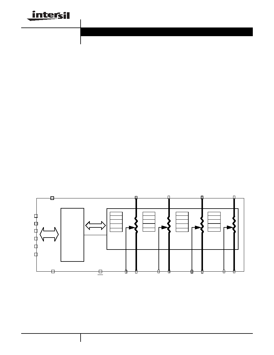
The X9259 integrates four digitally controlled potentio-
meters (XDCP) on a monolithic CMOS integrated circuit.
The digitally controlled potentiometers are imple-mented
with a combination of resistor elements and CMOS switches.
The position of the wipers are controlled by the user through
the 2-wire bus interface. Each potentiometer has associated
with it a volatile Wiper Counter Register (WCR) and four
non-volatile Data Registers that can be directly written to and
read by the user. The content of the WCR controls the
position of the wiper. At power-up, the device recalls the
content of the default Data Registers of each DCP (DR00,
DR10, DR20, and DR30) to the corresponding WCR.
The XDCP can be used as a three-terminal potentiometer or
as a two terminal variable resistor in a wide variety of
applications including control, parameter adjustments, and
signal processing.
Features
∑ Four Separate Potentiometers in One Package
∑ 256 Resistor Taps≠0.4% Resolution
∑ 2-Wire Serial Interface for Write, Read, and
Transfer Operations of the Potentiometer
∑ Wiper Resistance: 100
typical @ V
CC
= 5V
∑ 4 Non-volatile Data Registers for Each Potentiometer
∑ Non-volatile Storage of Multiple Wiper Positions
∑ Standby Current < 5µA Max
∑ V
CC
: 2.7V to 5.5V Operation
∑ 50k
, 100k versions of Total Resistance
∑ Endurance: 100,000 Data Changes per Bit per Register
∑ 100 yr. Data Retention
∑ Single Supply Version of X9258
∑ 24 Ld SOIC, 24 Ld TSSOP
∑ Low Power CMOS
∑ Pb-Free Plus Anneal Available (RoHS Compliant)
Functional Diagram
POWER UP,
INTERFACE
CONTROL
AND
V
CC
V
SS
2-Wire
R
H0
R
L0
DCP0
R
W0
A1
SDA
SCL
A3
A2
WP
WCR0
DR00
DR01
DR02
DR03
R
H1
R
L1
DCP1
R
W1
WCR1
DR10
DR11
DR12
DR13
R
H2
R
L2
DCP2
R
W2
WCR2
DR20
DR21
DR22
DR23
R
H3
R
L3
DCP3
R
W3
WCR3
DR30
DR31
DR32
DR33
A0
Interface
STATUS
Data Sheet
September 16, 2005
2
FN8169.2
September 16, 2005
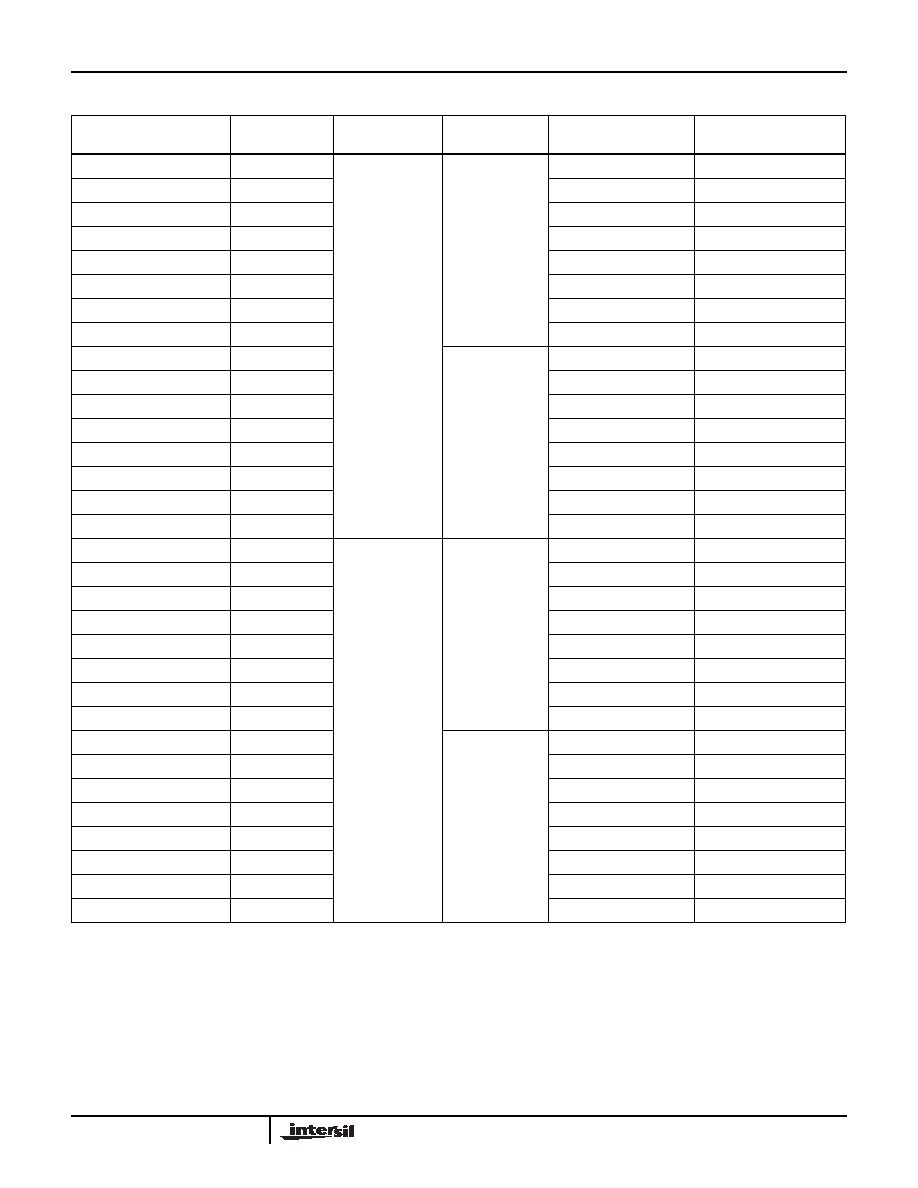
Ordering Information
PART
NUMBER
PART MARKING
V
CC
LIMITS
(V)
R
TOTAL
(k
)
TEMPERATURE RANGE
(∞C)
PACKAGE
X9259TS24*
X9259TS
5 ±10%
100
0 to 70
24 Ld SOIC
X9259TS24Z* (Note)
X9259TS Z
0 to 70
24 Ld SOIC (Pb-free)
X9259TS24I*
X9259TS I
-40 to 85
24 Ld SOIC
X9259TS24IZ* (Note)
X9259TS Z I
-40 to 85
24 Ld SOIC (Pb-free)
X9259TV24
X9259TV
0 to 70
24 Ld TSSOP
X9259TV24Z* (Note)
X9259TV Z
0 to 70
24 Ld TSSOP (Pb-free)
X9259TV24I
X9259TV I
-40 to 85
24 Ld TSSOP
X9259TV24IZ (Note)
X9259TV Z I
-40 to 85
24 Ld TSSOP (Pb-free)
X9259US24*
X9259US
50
0 to 70
24 Ld SOIC
X9259US24Z* (Note)
X9259US Z
0 to 70
24 Ld SOIC (Pb-free)
X9259US24I*
X9259US I
-40 to 85
24 Ld SOIC
X9259US24IZ* (Note)
X9259US Z I
-40 to 85
24 Ld SOIC (Pb-free)
X9259UV24
X9259UV
0 to 70
24 Ld TSSOP
X9259UV24Z (Note)
X9259UV Z
0 to 70
24 Ld TSSOP (Pb-free)
X9259UV24I*
X9259UV I
-40 to 85
24 Ld TSSOP
X9259UV24IZ* (Note)
X9259UV Z I
-40 to 85
24 Ld TSSOP (Pb-free)
X9259TS24-2.7*
X9259TS F
2.7-5.5
100
0 to 70
24 Ld SOIC
X9259TS24Z-2.7* (Note)
X9259TS Z F
0 to 70
24 Ld SOIC (Pb-free)
X9259TS24I-2.7*
X9259TS G
-40 to 85
24 Ld SOIC
X9259TS24IZ-2.7* (Note)
X9259TS Z G
-40 to 85
24 Ld SOIC (Pb-free)
X9259TV24-2.7
X9259TV F
0 to 70
24 Ld TSSOP
X9259TV24Z-2.7 (Note)
X9259TV Z F
0 to 70
24 Ld TSSOP (Pb-free)
X9259TV24I-2.7
X9259TV G
-40 to 85
24 Ld TSSOP
X9259TV24IZ-2.7 (Note)
X9259TV Z G
-40 to 85
24 Ld TSSOP (Pb-free)
X9259US24-2.7*
X9259US F
50
0 to 70
24 Ld SOIC
X9259US24Z-2.7* (Note)
X9259US Z F
0 to 70
24 Ld SOIC (Pb-free)
X9259US24I-2.7*
X9259US G
-40 to 85
24 Ld SOIC
X9259US24IZ-2.7* (Note)
X9259US Z G
-40 to 85
24 Ld SOIC (Pb-free)
X9259UV24-2.7*
X9259UV F
0 to 70
24 Ld TSSOP
X9259UV24Z-2.7 (Note)
X9259UV Z F
0 to 70
24 Ld TSSOP (Pb-free)
X9259UV24I-2.7*
X9259UV G
-40 to 85
24 Ld TSSOP
X9259UV24IZ-2.7* (Note)
X9259UV Z G
-40 to 85
24 Ld TSSOP (Pb-free)
NOTE: Intersil Pb-free plus anneal products employ special Pb-free material sets; molding compounds/die attach materials and 100% matte tin plate
termination finish, which are RoHS compliant and compatible with both SnPb and Pb-free soldering operations. Intersil Pb-free products are MSL
classified at Pb-free peak reflow temperatures that meet or exceed the Pb-free requirements of IPC/JEDEC J STD-020.
*Add "T1" suffix for tape and reel.
X9259
3
FN8169.2
September 16, 2005
Circuit Level Applications
∑ Vary the gain of a voltage amplifier
∑ Provide programmable dc reference voltages for
comparators and detectors
∑ Control the volume in audio circuits
∑ Trim out the offset voltage error in a voltage amplifier
circuit
∑ Set the output voltage of a voltage regulator
∑ Trim the resistance in Wheatstone bridge circuits
∑ Control the gain, characteristic frequency and
Q-factor in filter circuits
∑ Set the scale factor and zero point in sensor signal
conditioning circuits
∑ Vary the frequency and duty cycle of timer ICs
∑ Vary the dc biasing of a pin diode attenuator in RF circuits
∑ Provide a control variable (I, V, or R) in feedback
circuits
System Level Applications
∑ Adjust the contrast in LCD displays
∑ Control the power level of LED transmitters in
communication systems
∑ Set and regulate the DC biasing point in an RF power
amplifier in wireless systems
∑ Control the gain in audio and home entertainment systems
∑ Provide the variable DC bias for tuners in RF wireless
systems
∑ Set the operating points in temperature control
systems
∑ Control the operating point for sensors in industrial
systems
∑ Trim offset and gain errors in artificial intelligent
systems
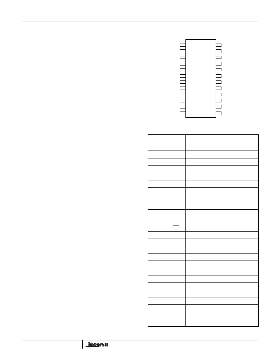
Pin Configuration
Pin Assignments
PIN
(SOIC/
TSSOP) SYMBOL
FUNCTION
2
A0
Device Address for 2-Wire bus. (See Note 1)
3
R
W3
Wiper Terminal of DCP3
4
R
H3
High Terminal of DCP3
5
R
L3
Low Terminal of DCP3
6
NC1
Must be left unconnected
7
V
CC
System Supply Voltage
8
R
L0
Low Terminal of DCP0
9
R
H0
High Terminal of DCP0
10
R
W0
Wiper Terminal of DCP0
11
A2
Device Address for 2-Wire bus. (See Note 1)
12
WP
Hardware Write Protect ≠ Active Low
13
SDA
Serial Data Input/Output for 2-Wire bus.
14
A1
Device Address for 2-Wire bus. (See Note 1)
15
R
L1
Low Terminal of DCP1
16
R
H1
High Terminal of DCP1
17
R
W1
Wiper Terminal of DCP1
18
V
SS
System Ground
20
R
W2
WiperTerminal of DCP2
21
R
H2
High Terminal of DCP2
22
R
L2
Low Terminal of DCP2
23
SCL
Serial Clock for 2-Wire bus.
24
A3
Device Address for 2-Wire bus. (See Note 1)
6, 19
NC
No Connect
1
DNC
Do Not Connect
Note 1: A0-A3 Device address pins must be tied to a logic level.
DNC
A0
R
W3
NC
V
CC
R
L0
1
2
3
4
5
6
7
8
9
10
24
23
22
21
20
19
18
17
16
15
A3
SCL
R
L2
R
H2
R
W2
NC
V
SS
R
W1
R
H1
R
L1
SOIC/TSSOP
X9259
R
H3
14
13
11
12
R
L3
R
H0
R
W0
A2
A1
SDA
WP
X9259

4
FN8169.2
September 16, 2005
Pin Descriptions
Bus Interface Pins
SERIAL DATA INPUT/OUTPUT (SDA)
The SDA is a bidirectional serial data input/output pin for a 2-
Wire slave device and is used to transfer data into and out of
the device. It receives device address, opcode, wiper
register address and data sent from a 2-Wire master at the
rising edge of the serial clock SCL, and it shifts out data after
each falling edge of the serial clock SCL.
It is an open drain output and may be wire-ORed with any
number of open drain or open collector outputs. An open
drain output requires the use of a pull-up resistor.
SERIAL CLOCK (SCL)
This input is used by 2-Wire master to supply 2-Wire serial
clock to the X9259.
DEVICE ADDRESS (A3 ≠ A0)
The Address inputs are used to set the least significant 4 bits
of the 8-bit slave address. A match in the slave address
serial data stream must be made with the Address input in
order to initiate communication with the X9259. A maximum
of 16 devices may occupy the 2-Wire serial bus. Device pins
A3-A0 must be tie to a logic level which specify the external
address of the device, see Figures 3, 4, and 5.
Potentiometer Pins
R
H
, R
L
The R
H
and R
L
pins are equivalent to the terminal
connections on a mechanical potentiometer. Since there are
4 potentiometers, there are 4 sets of R
H
and R
L
such that
R
H0
and R
L0
are the terminals of DCP0 and so on.
R
W
The wiper pin are equivalent to the wiper terminal of a
mechanical potentiometer. Since there are 4 potentiometers,
there are 4 sets of R
W
such that R
W0
is the terminal of
DCP0 and so on.
Bias Supply Pins
SYSTEM SUPPLY VOLTAGE (V
CC
) AND SUPPLY
GROUND (V
SS
)
The V
CC
pin is the system supply voltage. The V
SS
pin is
the system ground.
Other Pins
NO CONNECT
No connect pins should be left open. This pins are used for
Intersil manufacturing and testing purposes.
HARDWARE WRITE PROTECT INPUT (WP)
The WP pin when LOW prevents non-volatile writes to the
Data Registers.
SERIAL DATA PATH
FROM INTERFACE
CIRCUITRY
DR#0
SERIAL
BUS
INPUT
PARALLEL
BUS
INPUT
COUNTER
REGISTER
INC/DEC
LOGIC
UP/DN
CLK
MODIFIED SCK
UP/DN
8
8
COUNTER
IF WCR = 00[H] then R
W
is closest to R
L
IF WCR = FF[H] then R
W
is closest to R
H
WIPER
(WCR#)
#: 0, 1, 2, or 3
One of Four Potentiometers
DR#2
DR#1
DR#3
- - -
DECODE
DCP
CORE
R
W
R
H
R
L
FIGURE 1. DETAILED POTENTIOMETER BLOCK DIAGRAM
X9259
5
FN8169.2
September 16, 2005
Principles of Operation
The X9259 is an integrated circuit incorporating four DCPs
and their associated registers and counters, and the serial
interface providing direct communication between a host
and the potentiometers.
DCP Description
Each DCP is implemented with a combination of resistor
elements and CMOS switches. The physical ends of each
DCP are equivalent to the fixed terminals of a mechanical
potentiometer (R
H
and R
L
pins). The RW pin is an
intermediate node, equivalent to the wiper terminal of a
mechanical potentiometer.
The position of the wiper terminal within the DCP is
controlled by an 8-bit volatile Wiper Counter Register
(WCR).
Power Up and Down Recommendations
There are no restrictions on the power-up or power-down
conditions of V
CC
and the voltages applied to the
potentiometer pins provided that V
CC
is always more
positive than or equal to V
H
, V
L
, and V
W
, i.e., V
CC
V
H
, V
L
,
V
W
. The V
CC
ramp rate specification is always in effect.
Wiper Counter Register (WCR)
The X9259 contains four Wiper Counter Registers, one for
each potentiometer. The Wiper Counter Register can be
envisioned as a 8-bit parallel and serial load counter with its
outputs decoded to select one of 256 wiper positions along
its resistor array. The contents of the WCR can be altered in
four ways: it may be written directly by the host via the Write
Wiper Counter Register instruction (serial load); it may be
written indirectly by transferring the contents of one of four
associated data registers via the XFR Data Register
instruction (parallel load); it can be modified one step at a
time by the Increment/Decrement instruction (see Instruction
section for more details). Finally, it is loaded with the
contents of its data register zero (DR#0) upon power-up.
(See Figure 1.)
The Wiper Counter Register is a volatile register; that is, its
contents are lost when the X9259 is powered-down.
Although the register is automatically loaded with the value
in DR#0 upon power-up, this may be different from the value
present at power-down. Power-up guidelines are
recommended to ensure proper loadings of the DR#0 value
into the WCR# (See Design Considerations Section).
Data Registers (DR)
Each of the four DCPs has four 8-bit non-volatile Data
Registers. These can be read or written directly by the host.
Data can also be transferred between any of the four data
registers and the associated Wiper Counter Register. All
operations changing data in one of the data registers is a
non-volatile operation and takes a maximum of 10ms.
If the application does not require storage of multiple
settings for the potentiometer, the Data Registers can be
used as regular memory locations for system parameters or
user preference data.
Bit [7:0] are used to store one of the 256 wiper positions
(0~255).
TABLE 1. WIPER COUNTER REGISTER, WCR (8-bit), WCR[7:0]: Used to store the current wiper position (Volatile).
TABLE 2. DATA REGISTER, DR (8-BIT), BIT [7:0]: Used to store wiper positions or data (Non-volatile).
WCR7
WCR6
WCR5
WCR4
WCR3
WCR2
WCR1
WCR0
(MSB)
(LSB)
Bit 7
Bit 6
Bit 5
Bit 4
Bit 3
Bit 2
Bit 1
Bit 0
(MSB)
(LSB)
X9259

6
FN8169.2
September 16, 2005
Serial Interface
The X9259 supports a bidirectional bus oriented protocol.
The protocol defines any device that sends data onto the
bus as a transmitter and the receiving device as the receiver.
The device controlling the transfer is a master and the
device being controlled is the slave. The master always
initiates data transfers and provide the clock for both
transmit and receive operations. Therefore, the X9259
operates as a slave device in all applications.
All 2-wire interface operations must begin with a START,
followed by an Identification Byte, that selects the X9259. All
communication over the 2-wire interface is conducted by
sending the MSB of each byte of data first.
Clock and Data Conventions
Data states on the SDA line can change only during SCL
LOW periods. SDA state changes during SCL HIGH are
reserved for indicating START and STOP conditions. See
Figure 2. On power up of the X9259 the SDA pin is in the
input mode.
START Condition
All commands to the X9259 are preceded by the start
condition, which is a HIGH to LOW transition of SDA while
SCL is HIGH. The X9259 continuously monitors the SDA
and SCL lines for the START condition and does not
respond to any command until this condition is met. See
Figure 2.
STOP Condition
All communications must be terminated by a STOP
condition, which is a LOW to HIGH transition of SDA while
SCL is HIGH. See Figure 2. The STOP condition is also
used to place the device into the Standby Power mode after
a Read sequence. A STOP condition can only be issued
after the transmitting device has released the bus.
Acknowledge
An ACK, Acknowledge, is a software convention used to
indicate a successful data transfer. The transmitting device,
either master or slave, releases the SDA bus after
transmitting eight bits. During the ninth clock cycle, the
receiver pulls the SDA line LOW to acknowledge the
reception of the eight bits of data. See Figure 3.
The X9259 responds with an ACK after recognition of a
START condition followed by a valid Identification Byte, and
once again after successful receipt of an Instruction Byte.
The X9259 also responds with an ACK after receiving a Data
Byte after a Write Instruction.
A valid Identification Byte contains the Device Type Identifier
0101, as the four MSBs, and the Device Address bits
matching the logic states of pins A3, A2, A1, and A0, as the
four LSBs. See Figure 4.
In the Read mode, the device transmits eight bits of data,
releases the SDA line, and then monitors the line for an
ACK. The device continues transmitting data if an ACK is
detected. The device terminates further data transmissions if
an ACK is not detected. The master must then issue a STOP
condition to place the device into a known state.
During the internal non-volatile Write operation, the X9259
ignores the inputs at SDA and SCL, and does not issue an
ACK after Identification bytes.
X9259

7
FN8169.2
September 16, 2005
Identification Byte
The first byte sent to the X9259 from the host is called the
Identification Byte. The most significant four bits are a
Device Type Identifier, ID[3:0] bits, which must be 0101.
Refer to Table 3.
Only the device which Slave Address matches the incoming
device address sent by the master executes the instruction.
The A3 - A0 inputs can be actively driven by CMOS input
signals or tied to V
CC
or V
SS
.
INSTRUCTION BYTE (I)
The next byte sent to the X9259 contains the instruction and
register pointer information. The four most significant bits are
used provide the instruction opcode I [3:0]. The RB and RA
bits point to one of the four data registers of each associated
XDCP. The least two significant bits point to one of four
Wiper Counter Registers or DCPs. The format is shown in
Table 4.
Data Register Selection
#: 0, 1, 2, or 3
The least significant four bits of the Identification Byte are
the Slave Address bits, AD[3:0]. To access the X9259, these
four bits must match the logic values of pins A3, A2, A1, and
A0.
SDA
SCL
START
DATA
DATA
STOP
STABLE CHANGE
DATA
STABLE
FIGURE 2. VALID DATA CHANGES, START, AND STOP CONDITIONS
SDA Output from
Transmitter
SDA Output from
Receiver
8
1
9
START
ACK
SCL from
Master
FIGURE 3. ACKNOWLEDGE RESPONSE FROM RECEIVER
REGISTER
RB
RA
DR#0
0
0
DR#1
0
1
DR#2
1
0
DR#3
1
1
X9259
8
FN8169.2
September 16, 2005
TABLE 3. IDENTIFICATION BYTE FORMAT
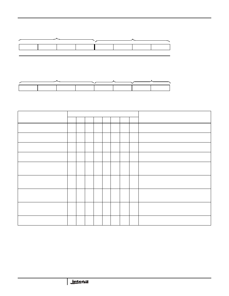
TABLE 4. INSTRUCTION BYTE FORMAT
Note:
1/0 = data is one or zero
ID3
ID2
ID1
ID0
A3
A2
A1
A0
0
1
0
1
Logic value of pins A3, A2, A1, and A0
(MSB)
(LSB)
Device Type
Identifier
Slave Address
I3
I2
I1
I0
RB
RA
P1
P0
(MSB)
(LSB)
Instruction
Register
DCP Selection
Opcode
Selection
(WCR Selection)
TABLE 5. INSTRUCTION SET
INSTRUCTION
INSTRUCTION SET
OPERATION
I3
I2
I1
I0
RB
RA
P1
P0
Read Wiper Counter
Register
1
0
0
1
0
0
1/0
1/0
Read the contents of the Wiper Counter Register
pointed to by P1 - P0
Write Wiper Counter Register
1
0
1
0
0
0
1/0
1/0
Write new value to the Wiper Counter
Register pointed to by P1 - P0
Read Data Register
1
0
1
1
1/0
1/0
1/0
1/0
Read the contents of the Data Register pointed to by
P1 - P0 and RB - RA
Write Data Register
1
1
0
0
1/0
1/0
1/0
1/0
Write new value to the Data Register
pointed to by P1 - P0 and RB - RA
XFR Data Register to Wiper
Counter Register
1
1
0
1
1/0
1/0
1/0
1/0
Transfer the contents of the Data Register pointed to
by P1 - P0 and RB - RA to its
associated Wiper Counter Register
XFR Wiper Counter Register to
Data Register
1
1
1
0
1/0
1/0
1/0
1/0
Transfer the contents of the Wiper Counter Register
pointed to by P1 - P0 to the Data Register pointed to
by RB - RA
Global XFR Data Registers to Wiper
Counter Registers
0
0
0
1
1/0
1/0
0
0
Transfer the contents of the Data Registers pointed to
by RB - RA of all four pots to their respective Wiper
Counter Registers
Global XFR Wiper Counter
Registers to Data Register
1
0
0
0
1/0
1/0
0
0
Transfer the contents of both Wiper Counter
Registers to their respective data Registers pointed to
by RB - RA of all four DCPs
Increment/Decrement Wiper
Counter Register
0
0
1
0
0
0
1/0
1/0
Enable Increment/decrement of the Control Latch
pointed to by P1 - P0
X9259
9
FN8169.2
September 16, 2005
Instructions
Four of the nine instructions are three bytes in length. These
instructions are:
∑ Read Wiper Counter Register ≠ read the current wiper
position of the selected potentiometer,
∑ Write Wiper Counter Register ≠ change current wiper
position of the selected potentiometer,
∑ Read Data Register ≠ read the contents of the selected
Data Register;
∑ Write Data Register ≠ write a new value to the selected
Data Register.
The basic sequence of the three byte instructions is
illustrated in Figure 5. These three-byte instructions
exchange data between the WCR and one of the Data
Registers. A transfer from a Data Register to a WCR is
essentially a write to a static RAM, with the static RAM
controlling the wiper position. The response of the wiper to
this action is delayed by t
WRL
. A transfer from the WCR
(current wiper position), to a Data Register is a write to non-
volatile memory and takes a minimum of t
WR
to complete.
The transfer can occur between one of the four
potentiometer's WCR, and one of its associated registers,
DRs; or it may occur globally, where the transfer occurs
between all potentiometers and one associated register.
Four instructions require a two-byte sequence to complete.
These instructions transfer data between the host and the
X9259; either between the host and one of the data registers
or directly between the host and the Wiper Counter Register.
These instructions are:
∑ XFR Data Register to Wiper Counter Register ≠ This
transfers the contents of one specified Data Register to
the associated Wiper Counter Register.
∑ XFR Wiper Counter Register to Data Register ≠ This
transfers the contents of the specified Wiper Counter
Register to the specified associated Data Register.
∑ Global XFR Data Register to Wiper Counter
Register ≠ This transfers the contents of all specified Data
Registers to the associated Wiper Counter Registers.
∑ Global XFR Wiper Counter Register to Data
Register ≠ This transfers the contents of all Wiper
Counter Registers to the specified associated Data
Registers.
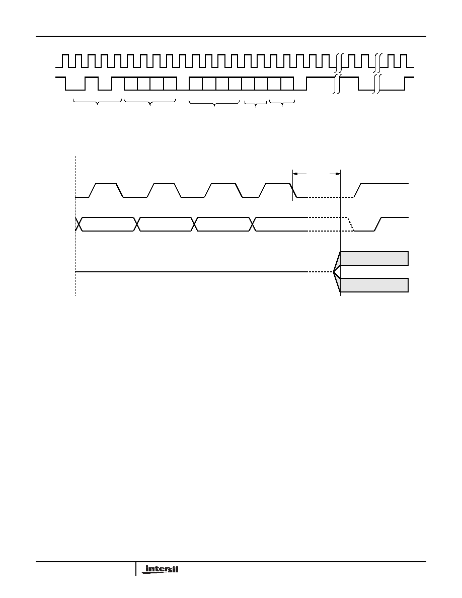
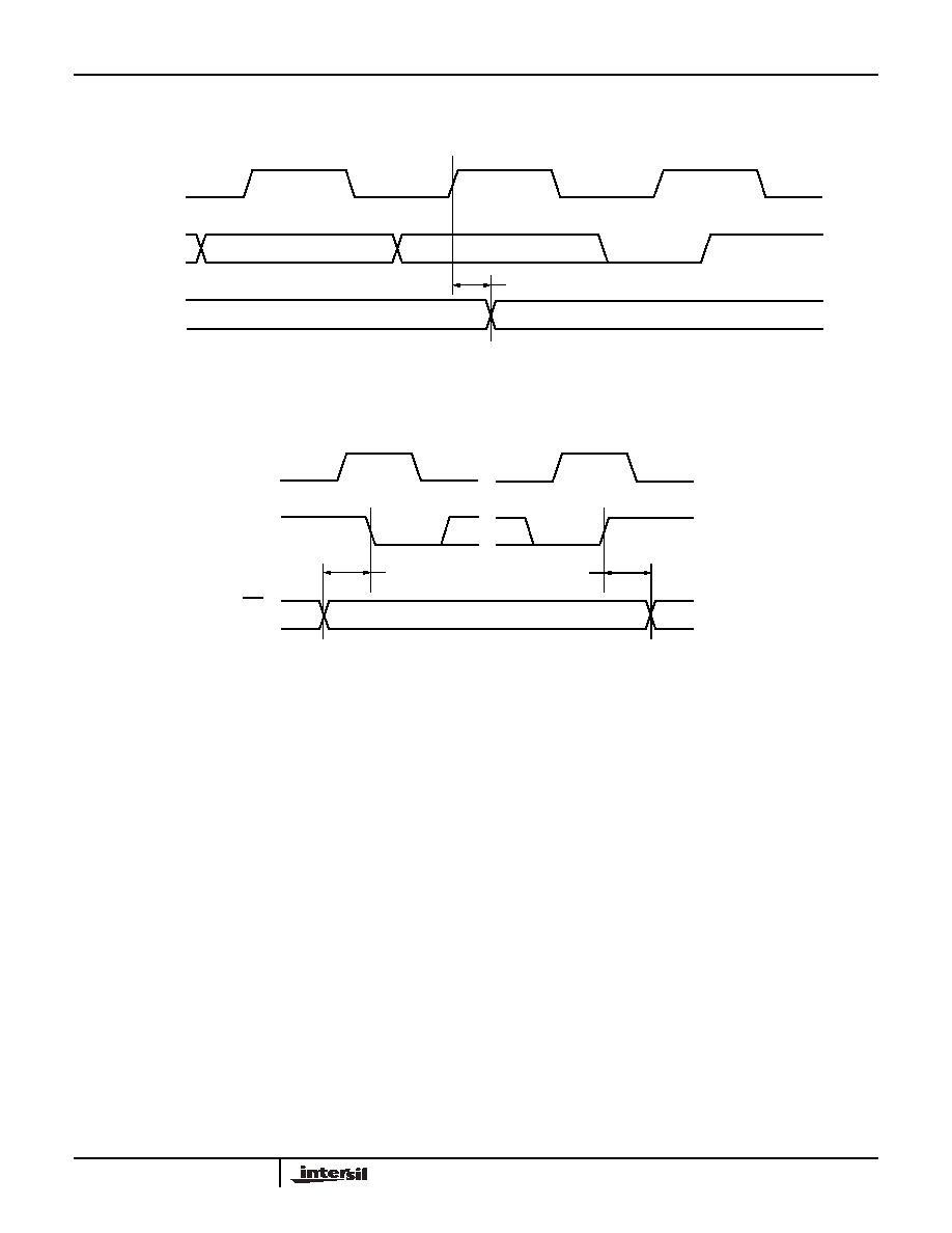
Increment/Decrement Command
The final command is Increment/Decrement (Figure 6 and
7). The Increment/Decrement command is different from the
other commands. Once the command is issued and the
X9259 has responded with an Acknowledge, the master can
clock the selected wiper up and/or down in one segment
steps; thereby, providing a fine tuning capability to the host.
For each SCL clock pulse (t
HIGH
) while SDA is HIGH, the
selected wiper moves one wiper position towards the R
H
terminal. Similarly, for each SCL clock pulse while SDA is
LOW, the selected wiper moves one resistor wiper position
towards the R
L
terminal.
See Instruction format for more details.
S
T
A
R
T
0
1
0
1
A2
A0
A
C
K
I2 I1 I0
RB RA P1
A
C
K
SCL
SDA
S
T
O
P
ID3 ID2 ID1 ID0
P0
Device ID
External
Instruction
Opcode
Address
Register
Address
DCP/WCR
Address
A1
A3
I3
FIGURE 4. TWO-BYTE INSTRUCTION SEQUENCE
I3
I2 I1 I0
RB RA
ID3 ID2 ID1ID0
Device ID
External
Instruction
Opcode
Address
Register
Address
Pot/WCR
Address
Data for WCR[7:0] or DR[7:0]
S
T
A
R
T
0
1
0
1
A2 A1 A0 A
C
K
P1 P0 A
C
K
SCL
SDA
S
T
O
P
A
C
K
D7 D6 D5 D4 D3 D2 D1 D0
A3
FIGURE 5. THREE-BYTE INSTRUCTION SEQUENCE 2-WIRE INTERFACE
X9259
10
FN8169.2
September 16, 2005
I3
I2
I1
I0
ID3 ID2 ID1 ID0
Device ID
External
Instruction
Opcode
Address
Register
Address
Pot/WCR
Address
S
T
A
R
T
0
1
0
1
A2 A1 A0
A
C
K
RA P1 P0 A
C
K
SCL
SDA
S
T
O
P
I
N
C
1
I
N
C
2
I
N
C
n
D
E
C
1
D
E
C
n
RB
A3
FIGURE 6. INCREMENT/DECREMENT INSTRUCTION SEQUENCE 2-WIRE INTERFACE
SCL
SDA
R
W
INC/DEC
CMD
Issued
Voltage Out
t
WRID
FIGURE 7. INCREMENT/DECREMENT TIMING SPEC
X9259
11
FN8169.2
September 16, 2005
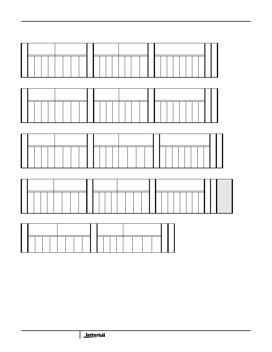
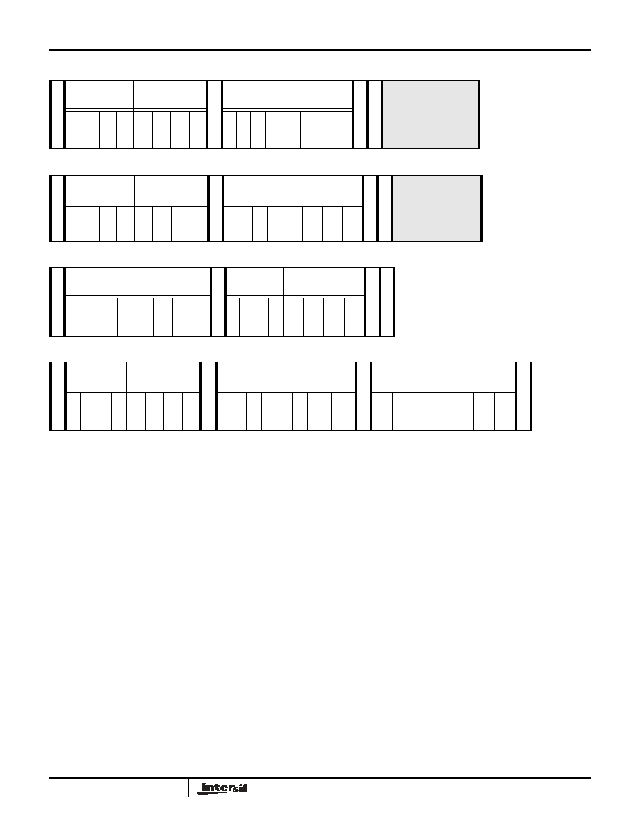
Instruction Format
Read Wiper Counter Register (WCR)
Write Wiper Counter Register (WCR)
Read Data Register (DR)
Write Data Register (DR)
Global XFR Data Register (DR) to Wiper Counter Register (WCR)
Notes: (1) "MACK"/"SACK": stands for the acknowledge sent by the Master/Slave.
(2) "A3 ~ A0": stands for the device addresses sent by the master.
(3) "X": indicates that it is a "0" for testing purpose but physically it is a "don't care" condition.
(4) "I": stands for the increment operation, SDA held high during active SCL phase (high).
(5) "D": stands for the decrement operation, SDA held low during active SCL phase (high).
S
T
A
R
T
Device Type
Identifier
Device
Addresses
S
A
C
K
Instruction
Opcode
DR/WCR
Addresses
S
A
C
K
Wiper Position
(Sent by X9259 on SDA) M
A
C
K
S
T
O
P
0 1 0 1 A3 A2 A1 A0
1 0 0 1 0 0 P1 P0
W
C
R
7
W
C
R
6
W
C
R
5
W
C
R
4
W
C
R
3
W
C
R
2
W
C
R
1
W
C
R
0
S
T
A
R
T
Device Type
Identifier
Device
Addresses
S
A
C
K
Instruction
Opcode
DR/WCR
Addresses
S
A
C
K
Wiper Position
(Sent by Master on SDA) S
A
C
K
S
T
O
P
0 1 0 1 A3 A2 A1 A0
1 0 1 0 0 0 P1 P0
W
C
R
7
W
C
R
6
W
C
R
5
W
C
R
4
W
C
R
3
W
C
R
2
W
C
R
1
W
C
R
0
S
T
A
R
T
Device Type
Identifier
Device
Addresses
S
A
C
K
Instruction
Opcode
DR/WCR
Addresses
S
A
C
K
Wiper Position
(Sent by X9259 on SDA) M
A
C
K
S
T
O
P
0 1 0 1 A3 A2 A1 A0
1 0 1 1 RB RA P1 P0
W
C
R
7
W
C
R
6
W
C
R
5
W
C
R
4
W
C
R
3
W
C
R
2
W
C
R
1
W
C
R
0
S
T
A
R
T
Device Type
Identifier
Device
Addresses
S
A
C
K
Instruction
Opcode
DR/WCR
Addresses
S
A
C
K
Wiper Position
(Sent by Master on SDA) S
A
C
K
S
T
O
P
HIGH-VOLTAGE
WR
ITE CYCLE
0 1 0 1 A3 A2 A1 A0
1 1 0 0 RB RA P1 P0
W
C
R
7
W
C
R
6
W
C
R
5
W
C
R
4
W
C
R
3
W
C
R
2
W
C
R
1
W
C
R
0
S
T
A
R
T
Device Type
Identifier
Device
Addresses
S
A
C
K
Instruction
Opcode
DR/WCR
Addresses
S
A
C
K
S
T
O
P
0
1
0
1 A3 A2 A1 A0
0 0 0 1 RB RA
0
0
X9259
12
FN8169.2
September 16, 2005
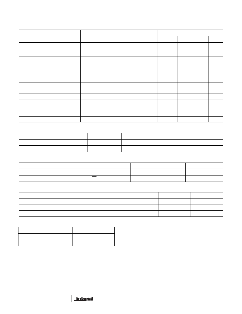
Global XFR Wiper Counter Register (WCR) to Data Register (DR)
Transfer Wiper Counter Register (WCR) to Data Register (DR)
Transfer Data Register (DR) to Wiper Counter Register (WCR)
Increment/Decrement Wiper Counter Register (WCR)
Notes: (1) "MACK"/"SACK": stands for the acknowledge sent by the Master/Slave.
(2) "A3 ~ A0": stands for the device addresses sent by the master.
(3) "X": indicates that it is a "0" for testing purpose but physically it is a "don't care" condition.
(4) "I": stands for the increment operation, SDA held high during active SCL phase (high).
(5) "D": stands for the decrement operation, SDA held low during active SCL phase (high).
S
T
A
R
T
Device Type
Identifier
Device
Addresses
S
A
C
K
Instruction
Opcode
DR/WCR
Addresses
S
A
C
K
S
T
O
P
HIGH-VOLTAGE
WRITE CYCLE
0
1
0
1 A3 A2 A1 A0
1 0 0 0 RB RA 0 0
S
T
A
R
T
Device Type
Identifier
Device
Addresses
S
A
C
K
Instruction
Opcode
DR/WCR
Addresses
S
A
C
K
S
T
O
P
HIGH-VOLTAGE
WRITE CYCLE
0
1
0
1 A3 A2 A1 A0
1 1 1 0 RB RA P1 P0
S
T
A
R
T
Device Type
Identifier
Device
Addresses
S
A
C
K
Instruction
Opcode
DR/WCR
Addresses
S
A
C
K
S
T
O
P
0
1
0
1 A3 A2 A1 A0
1 1 0 1 RB RA P1 P0
S
T
A
R
T
Device Type
Identifier
Device
Addresses
S
A
C
K
Instruction
Opcode
DR/WCR
Addresses
S
A
C
K
Increment/Decrement
(Sent by Master on SDA)
S
T
O
P
0 1 0 1 A3 A2 A1 A0
0 0 1 0 0 0 P1 P0
I/D I/D .
.
.
. I/D I/D
X9259

13
FN8169.2
September 16, 2005
Notes: (1) Absolute linearity is utilized to determine actual wiper voltage versus expected voltage as determined by wiper position when used as a
potentiometer.
(2) Relative linearity is utilized to determine the actual change in voltage between two successive tap positions when used as a
potentiometer. It is a measure of the error in step size.
(3) MI = RTOT / 255 or (R
H
≠ R
L
) / 255, single pot
(4) During power up V
CC
> V
H
, V
L
, and V
W
.
(5) n = 0, 1, 2, ...,255; m =0, 1, 2, ..., 254.
Absolute Maximum Ratings
Recommended Operating Conditions
Temperature under bias . . . . . . . . . . . . . . . . . . . . . .-65
∞C to +135∞C
Storage temperature . . . . . . . . . . . . . . . . . . . . . . . .-65
∞C to +150∞C
Voltage on SCL, SDA, any address input, V
CC
with respect to V
SS
. . . . . . . . . . . . . . . . . . . . . . . . . . . . . -1V to +7V
V = | (V
H
≠V
L
) | . . . . . . . . . . . . . . . . . . . . . . . . . . . . . . . . . . . . . 5.5V
Lead temperature (soldering, 10 seconds) . . . . . . . . . . . . . . . 300
∞C
I
W
(10 seconds) . . . . . . . . . . . . . . . . . . . . . . . . . . . . . . . . . . . ±6mA
Temperature (Commercial) . . . . . . . . . . . . . . . . . . . . . 0∞C to +70∞C
Temperature (Industrial). . . . . . . . . . . . . . . . . . . . . . .-40∞C to +85∞C
Supply Voltage (V
CC
) (Note 4) Limits
X9259. . . . . . . . . . . . . . . . . . . . . . . . . . . . . . . . . . . . . . . 5V ± 10%
X9259-2.7. . . . . . . . . . . . . . . . . . . . . . . . . . . . . . . . . . 2.7V to 5.5V
CAUTION: Stresses above those listed under "Absolute Maximum Ratings" may cause permanent damage to the device. This is a stress rating only; the functional
operation of the device (at these or any other conditions above those listed in the operational sections of this specification) is not implied. Exposure to absolute maximum
rating conditions for extended periods may affect device reliability.
Analog Specifications
Over recommended industrial (2.7V) operating conditions unless otherwise stated.
SYMBOL
PARAMETER
TEST CONDITIONS
LIMITS
MIN
TYP
MAX
UNITS
R
TOTAL
End to End Resistance
T version
100
k
R
TOTAL
End to End Resistance
U version
50
k
End to End Resistance Tolerance
±20
%
Power Rating
25
∞C, each pot
50
mW
I
W
Wiper Current
±3
mA
R
W
Wiper Resistance
I
W
=
@ V
CC
= 3V
300
I
W
=
@ V
CC
= 5V
150
V
TERM
Voltage on any R
H
or R
L
Pin
V
SS
= 0V
V
SS
V
CC
V
Noise
Ref: 1V
-120
dB
/Hz
Resolution
0.4
%
Absolute Linearity
(1)
R
w(n)(actual)
- R
w(n)(expected)
(5)
-1
+1
MI
(3)
Relative Linearity
(2)
R
w(n + 1)
- [R
w(n) + MI
]
(5)
-0.6
+0.6
MI
(3)
Temperature Coefficient of R
TOTAL
±300
ppm/
∞C
Ratiometric Temp. Coefficient
-20
+20
ppm/∞C
C
H
/C
L
/C
W
Potentiometer Capacitances
See Macro model
10/10/25
pF
V(V
CC
)
R
TOTAL
V(V
CC
)
R
TOTAL
X9259
14
FN8169.2
September 16, 2005
Notes: (6) This parameter is not 100% tested
(7) t
PUR
and t
PUW
are the delays required from the time the (last) power supply (V
CC
-) is stable until the specific instruction can be issued.
These parameters are periodically sampled and not 100% tested.
DC Electrical Specifications
Over the recommended operating conditions unless otherwise specified.
SYMBOL
PARAMETER
TEST CONDITIONS
LIMITS
MIN
TYP
MAX
UNITS
I
CC1
V
CC
supply current
(active)
f
SCL
= 400kHz; V
CC
= +6V;
SDA = Open; (for 2-Wire, Active, Read and
Volatile Write States only)
3
mA
I
CC2
V
CC
supply current
(non-volatile write)
f
SCL
= 400kHz; V
CC
= +6V;
SDA = Open; (for 2-Wire, Active,
Non-volatile Write State only)
5
mA
I
SB
V
CC
current (standby)
V
CC
= +6V; V
IN
= V
SS
or V
CC
; SDA = V
CC
;
(for 2-Wire, Standby State only)
5
µA
I
LI
Input leakage current
V
IN
= V
SS
to V
CC
10
µA
I
LO
Output leakage current
V
OUT
= V
SS
to V
CC
10
µA
V
IH
Input HIGH voltage
V
CC
x 0.7
V
CC
+ 1
V
V
IL
Input LOW voltage
-1
V
CC
x 0.3
V
V
OL
Output LOW voltage
I
OL
= 3mA
0.4
V
V
OH
Output HIGH voltage
I
OH
= -1mA, V
CC
+3V
V
CC
- 0.8
V
V
OH
Output HIGH voltage
I
OH
= -0.4mA, V
CC
+3V
V
CC
- 0.4
V
Endurance and Data Retention
PARAMETER
MIN
UNITS
Minimum endurance
100,000
Data changes per bit per register
Data retention
100
years
Capacitance
SYMBOL
TEST
MAX
UNITS
TEST CONDITIONS
C
IN/OUT
(6)
Input / Output capacitance (SDA)
8
pF
V
OUT
= 0V
C
IN
(6)
Input capacitance (SCL, WP, A2, A1 and A0)
6
pF
V
IN
= 0V
Power-up Timing
SYMBOL
PARAMETER MIN
MAX
UNITS
tr VCC
(6)
V
CC
Power-up rate
0.2
50
V/ms
tPUR
(7)
Power-up to initiation of read operation
1
ms
tPUW
(7)
Power-up to initiation of write operation
50
ms
A.C. Test Conditions
Input Pulse Levels
V
CC
x 0.1 to V
CC
x 0.9
Input rise and fall times
10ns
Input and output timing level
V
CC
x 0.5
X9259

15
FN8169.2
September 16, 2005
Equivalent A.C. Load Circuit
5V
1533
100pF
SDA pin
R
H
10pF
C
L
C
L
R
W
R
TOTAL
C
W
25pF
10pF
R
L
SPICE Macromodel
AC Timing
SYMBOL
PARAMETER
MIN
MAX
UNITS
f
SCL
Clock Frequency
400
kHz
t
CYC
Clock Cycle Time
2500
ns
t
HIGH
Clock High Time
600
ns
t
LOW
Clock Low Time
1300
ns
t
SU:STA
Start Setup Time
600
ns
t
HD:STA
Start Hold Time
600
ns
t
SU:STO
Stop Setup Time
600
ns
t
SU:DAT
SDA Data Input Setup Time
100
ns
t
HD:DAT
SDA Data Input Hold Time
30
ns
t
R
SCL and SDA Rise Time
300
ns
t
F
SCL and SDA Fall Time
300
ns
t
AA
SCL Low to SDA Data Output Valid Time
0.9
µs
t
DH
SDA Data Output Hold Time
0
ns
T
I
Noise Suppression Time Constant at SCL and SDA inputs
50
ns
t
BUF
Bus Free Time (Prior to Any Transmission)
1200
ns
t
SU:WPA
A0, A1 Setup Time
0
ns
t
HD:WPA
A0, A1 Hold Time
0
ns
High-Voltage Write Cycle Timing
SYMBOL
PARAMETER
TYP
MAX
UNITS
t
WR
High-voltage write cycle time (store instructions)
5
10
ms
XDCP Timing
SYMBOL
PARAMETER
MIN.
MAX.
UNITS
t
WRPO
Wiper response time after the third (last) power supply is stable
5
10
µs
t
WRL
Wiper response time after instruction issued (all load instructions)
5
10
µs
X9259

16
FN8169.2
September 16, 2005
Symbol Table
.
Timing Diagrams
Start and Stop Timing
Input Timing
Output Timing
WAVEFORM
INPUTS
OUTPUTS
Must be
steady
Will be
steady
May change
from Low to
High
Will change
from Low to
High
May change
from High to
Low
Will change
from High to
Low
Don't Care:
Changes
Allowed
Changing:
State Not
Known
N/A
Center Line
is High
Impedance
t
SU:STA
t
HD:STA
t
SU:STO
SCL
SDA
t
R
(START)
(STOP)
t
F
t
R
t
F
SCL
SDA
t
HIGH
t
LOW
t
CYC
t
HD:DAT
t
SU:DAT
t
BUF
SCL
SDA
t
DH
t
AA
X9259
17
FN8169.2
September 16, 2005
XDCP Timing (for All Load Instructions)
Write Protect and Device Address Pins Timing
SCL
SDA
VWx
(STOP)
LSB
t
WRL
SDA
SCL
...
...
...
WP
A0, A1
t
SU:WPA
t
HD:WPA
(START)
(STOP)
(Any Instruction)
X9259
18
FN8169.2
September 16, 2005
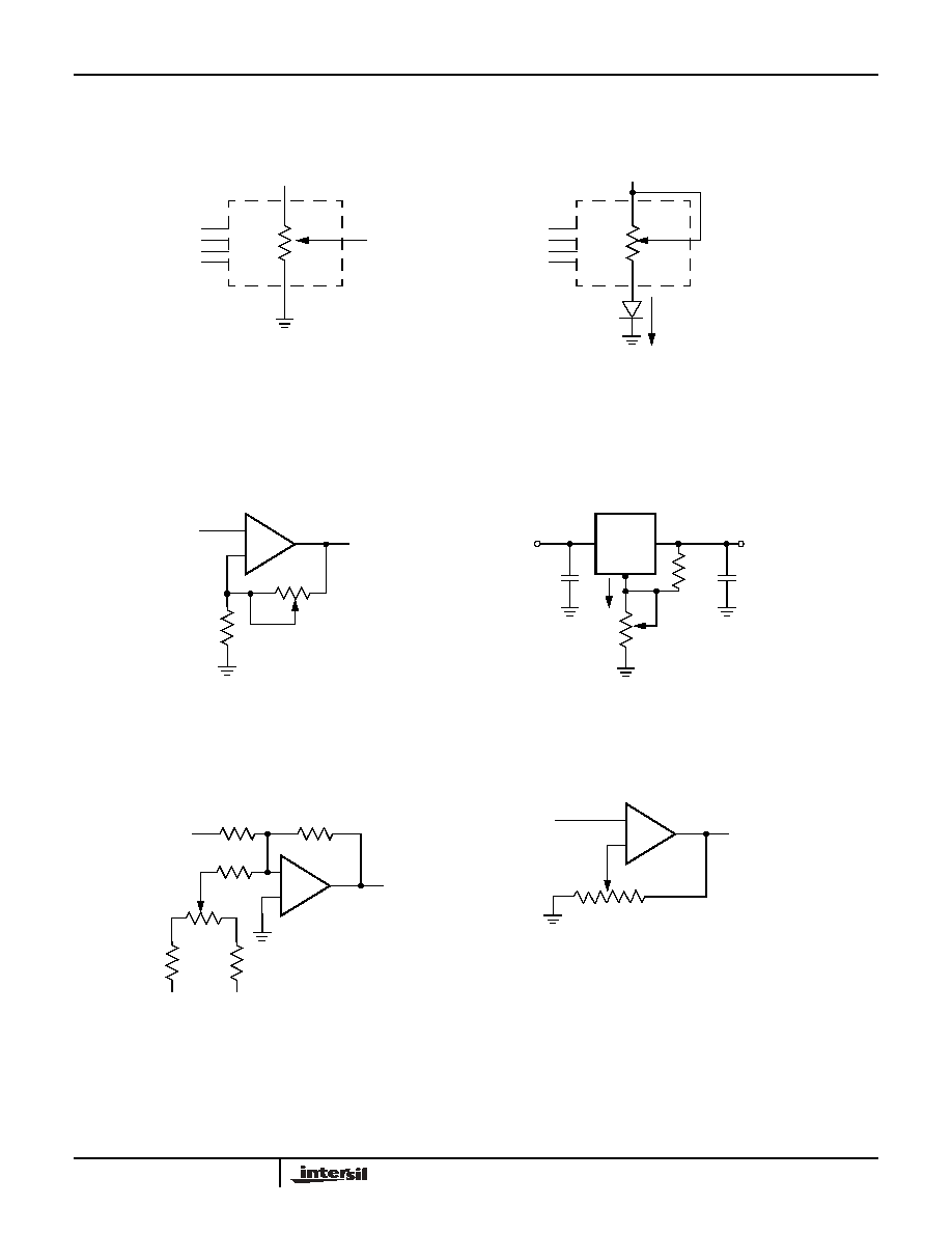
Applications Information
Basic Configurations of Electronic Potentiometers
Application Circuits
V
R
RW
+V
R
I
Three terminal
Potentiometer;
Variable voltage divider
Two terminal Variable
Resistor;
Variable current
Noninverting Amplifier
Voltage Regulator
Offset Voltage Adjustment
Comparator with Hysterisis
+
≠
V
S
V
O
R
2
R
1
V
O
= (1+R
2
/R
1
)V
S
R
1
R
2
I
adj
V
O
(REG) = 1.25V (1+R
2
/R
1
)+I
adj
R
2
V
O
(REG)
V
IN
317
+
≠
V
S
V
O
R
2
R
1
V
UL
= {R
1
/(R
1
+R
2
)} V
O
(max)
RL
L
= {R
1
/(R
1
+R
2
)} V
O
(min)
100k
10k
10k
10k
-12V
+12V
TL072
+
≠
V
S
V
O
R
2
R
1
}
}
X9259

19
FN8169.2
September 16, 2005
Application Circuits (continued)
Attenuator
Filter
Inverting Amplifier
Equivalent L-R Circuit
+
≠
V
S
V
O
R
3
R
1
V
O
= G V
S
-1/2
G +1/2
G
O
= 1 + R
2
/R
1
fc = 1/(2
RC)
+
≠
V
S
V
O
R
2
R
1
Z
IN
= R
2
+ s R
2
(R
1
+ R
3
) C
1
= R
2
+ s Leq
(R
1
+ R
3
) >> R
2
+
≠
V
S
Function Generator
R
2
R
4
R
1
= R
2
= R
3
= R
4
= 10k
+
≠
V
S
R
2
R
1
R
C
}
}
V
O
= G V
S
G = - R
2
/R
1
R
2
C
1
R
1
R
3
Z
IN
+
≠
R
2
+
≠
R
1
}
}
R
A
R
B
frequency
R
1
, R
2
, C
amplitude
R
A
, R
B
C
V
O
X9259
20
FN8169.2
September 16, 2005
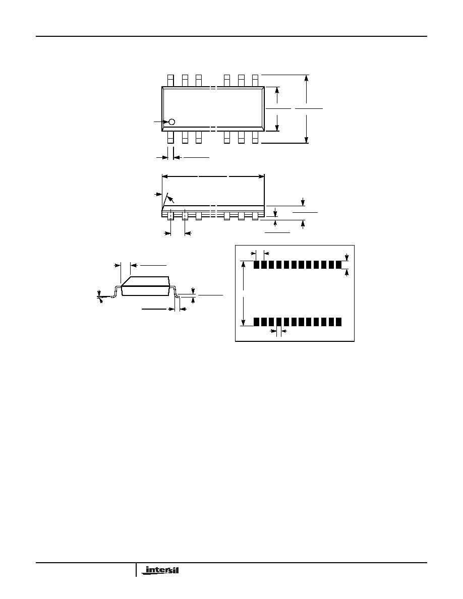
Packaging Information
0.290 (7.37)
0.299 (7.60)
0.393 (10.00)
0.420 (10.65)
0.014 (0.35)
0.020 (0.50)
Pin 1
Pin 1 Index
0.050 (1.27)
0.598 (15.20)
0.610 (15.49)
0.003 (0.10)
0.012 (0.30)
0.092 (2.35)
0.105 (2.65)
(4X) 7∞
24-Lead Plastic, SOIC, Package Code S24
NOTE: ALL DIMENSIONS IN INCHES (IN PARENTHESES IN MILLIMETERS)
0.420"
0.050" Typical
0.050"
Typical
0.030" Typical
24 Places
FOOTPRINT
0.010 (0.25)
0.020 (0.50)
0.015 (0.40)
0.050 (1.27)
0.009 (0.22)
0.013 (0.33)
0∞ - 8∞
X 45∞
X9259
21
All Intersil U.S. products are manufactured, assembled and tested utilizing ISO9000 quality systems.
Intersil Corporation's quality certifications can be viewed at www.intersil.com/design/quality
Intersil products are sold by description only. Intersil Corporation reserves the right to make changes in circuit design, software and/or specifications at any time without
notice. Accordingly, the reader is cautioned to verify that data sheets are current before placing orders. Information furnished by Intersil is believed to be accurate and
reliable. However, no responsibility is assumed by Intersil or its subsidiaries for its use; nor for any infringements of patents or other rights of third parties which may result
from its use. No license is granted by implication or otherwise under any patent or patent rights of Intersil or its subsidiaries.
For information regarding Intersil Corporation and its products, see www.intersil.com
FN8169.2
September 16, 2005
Packaging Information
NOTE: ALL DIMENSIONS IN INCHES (IN PARENTHESES IN MILLIMETERS)
24-Lead Plastic, TSSOP, Package Code V24
.169 (4.3)
.177 (4.5)
.252 (6.4) BSC
.026 (.65) BSC
.303 (7.70)
.311 (7.90)
.002 (.06)
.005 (.15)
.047 (1.20)
.0075 (.19)
.0118 (.30)
See Detail "A"
.031 (.80)
.041 (1.05)
.010 (.25)
.020 (.50)
.030 (.75)
Gage Plane
Seating Plane
Detail A (20X)
(4.16) (7.72)
(1.78)
(0.42)
(0.65)
ALL MEASUREMENTS ARE TYPICAL
0∞ - 8∞
X9259