 | –≠–ª–µ–∫—Ç—Ä–æ–Ω–Ω—ã–π –∫–æ–º–ø–æ–Ω–µ–Ω—Ç: X9313USM | –°–∫–∞—á–∞—Ç—å:  PDF PDF  ZIP ZIP |
1
Æ
FN8177.2
CAUTION: These devices are sensitive to electrostatic discharge; follow proper IC Handling Procedures.
1-888-INTERSIL or 1-888-468-3774
|
Intersil (and design) is a registered trademark of Intersil Americas Inc.
XDCP is a trademark of Intersil Americas Inc. Copyright Intersil Americas Inc. 2005. All Rights Reserved
All other trademarks mentioned are the property of their respective owners.
X9313
Terminal Voltages ±5V, 32 Taps
Digitally Controlled Potentiometer
(XDCPTM)
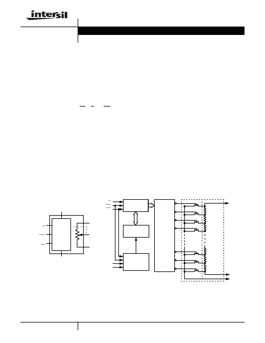
The Intersil X9313 is a digitally controlled potentiometer
(XDCP). The device consists of a resistor array, wiper
switches, a control section, and nonvolatile memory. The
wiper position is controlled by a 3-wire interface.
The potentiometer is implemented by a resistor array
composed of 31 resistive elements and a wiper switching
network. Between each element and at either end are tap
points accessible to the wiper terminal. The position of the
wiper element is controlled by the CS, U/D, and INC inputs.
The position of the wiper can be stored in nonvolatile
memory and then be recalled upon a subsequent power-up
operation.
The device can be used as a three-terminal potentiometer or
as a two-terminal variable resistor in a wide variety of
applications including:
∑ Control
∑ Parameter adjustments
∑ Signal processing
Features
∑ Solid-state potentiometer
∑ 3-wire serial interface
∑ 32 wiper tap points
- Wiper position stored in nonvolatile memory and
recalled on power-up
∑ 31 resistive elements
- Temperature compensated
- End to end resistance range ± 20%
- Terminal voltages, -5V to +5V
∑ Low power CMOS
- V
CC
= 3V or 5V
- Active current, 3mA max.
- Standby current, 500µA max.
∑ High reliability
- Endurance, 100,000 data changes per bit
- Register data retention, 100 years
∑ R
TOTAL
values = 1k
, 10k, 50k
∑ Packages
- 8 Ld SOIC, MSOP and DIP
∑ Pb-free plus anneal available (RoHS compliant)
Block Diagrams
5-BIT
NONVOLATILE
MEMORY
STORE AND
RECALL
CONTROL
CIRCUITRY
ONE
OF
DECODER
RESISTOR
ARRAY
R
H
/V
H
U/D
INC
CS
TRANSFER
GATES
THIRTY
V
CC
V
SS
R
L
/V
L
R
W
/V
W
CONTROL
UP/DOWN
V
CC
(SUPPLY VOLTAGE)
V
SS
(GROUND)
R
H
/V
H
R
W
/V
W
R
L
/V
L
GENERAL
DETAILED
0
1
2
28
29
30
31
TWO
(U/D)
INCREMENT
(INC)
DEVICE SELECT
(CS)
AND
MEMORY
5-BIT
UP/DOWN
COUNTER
Data Sheet
September 9, 2005
2
FN8177.2
September 9, 2005
Ordering Information
PART NUMBER
PART MARKING
V
CC
RANGE
(V)
R
TOTAL
(k
)
TEMPERATURE
RANGE
(∞C)
PACKAGE
X9313UM*
313U
4.5 to 5.5
50
0 to 70
8 Ld MSOP
X9313UMZ* (Note)
DDC
0 to 70
8 Ld MSOP (Pb-free)
X9313UMI*
13UI
-40 to 85
8 Ld MSOP
X9313UMIZ* (Note)
DDB
-40 to 85
8 Ld MSOP (Pb-free)
X9313UP
X9313UP
0 to 70
8 Ld PDIP
X9313UPI
X9313UP I
-40 to 85
8 Ld PDIP
X9313US*
X9313U
0 to 70
8 Ld SOIC
X9313USZ* (Note)
X9313U Z
0 to 70
8 Ld SOIC (Pb-free)
X9313USI*
X9313U I
-40 to 85
8 Ld SOIC
X9313USIZ* (Note)
X9313U Z I
-40 to 85
8 Ld SOIC (Pb-free)
X9313USM
0 to 70
8 Ld SOIC
X9313WM*
313W
10
0 to 70
8 Ld MSOP
X9313WMZ* (Note)
DDF
0 to 70
8 Ld MSOP (Pb-free)
X9313WMI*
13WI
-40 to 85
8 Ld MSOP
X9313WMIZ* (Note)
DDE
-40 to 85
8 Ld MSOP (Pb-free)
X9313WP
X9313WP
0 to 70
8 Ld PDIP
X9313WPI
X9313XP I
-40 to 85
8 Ld PDIP
X9313WS*
X9313WS
0 to 70
8 Ld SOIC
X9313WSZ* (Note)
X9313W Z
0 to 70
8 Ld SOIC (Pb-free)
X9313WSI*
X9313WS I
-40 to 85
8 Ld SOIC
X9313WSIZ* (Note)
X9313WS Z I
-40 to 85
8 Ld SOIC (Pb-free)
X9313WSMT2
X9313WS M
0 to 70
8 Ld SOIC Tape and Reel
X9313ZM*
313Z
0 to 70
8 Ld MSOP
X9313ZMZ* (Note)
DDJ
0 to 70
8 Ld MSOP (Pb-free)
X9313ZMI*
13ZI
1
-40 to 85
8 Ld MSOP
X9313ZMIZ* (Note)
DDH
-40 to 85
8 Ld MSOP (Pb-free)
X9313ZP
X9313ZP
0 to 70
8 Ld PDIP
X9313ZPI
X9313ZP I
-40 to 85
8 Ld PDIP
X9313ZS*
X9313ZS
0 to 70
8 Ld SOIC
X9313ZSZ* (Note)
X9313 Z
0 to 70
8 Ld SOIC (Pb-free)
X9313ZSI*
X9313ZS I
-40 to 85
8 Ld SOIC
X9313ZSIZ* (Note)
X9313ZS Z I
-40 to 85
8 Ld SOIC (Pb-free)
X9313
3
FN8177.2
September 9, 2005
X9313UM-3*
13UD
3 to 5.5
50
0 to 70
8 Ld MSOP
X9313UMZ-3* (Note)
DDD
0 to 70
8 Ld MSOP (Pb-free)
X9313UMI-3*
13UE
-40 to 85
8 Ld MSOP
X9313UMIZ-3* (Note)
13UE Z
-40 to 85
8 Ld MSOP (Pb-free)
X9313UP-3
X9313UP D
0 to 70
8 Ld PDIP
X9313US-3*
X9313U D
0 to 70
8 Ld SOIC
X9313USZ-3* (Note)
X9313U Z D
0 to 70
8 Ld SOIC (Pb-free)
X9313WM-3*
13WD
10
0 to 70
8 Ld MSOP
X9313WMZ-3* (Note)
DDG
0 to 70
8 Ld MSOP (Pb-free)
X9313WMI-3*
13WE
-40 to 85
8 Ld MSOP
X9313WMIZ-3* (Note)
13WE Z
-40 to 85
8 Ld MSOP (Pb-free)
X9313WP-3
X9313WP D
0 to 70
8 Ld PDIP
X9313WS-3*
X9313W D
0 to 70
8 Ld SOIC
X9313WSZ-3* (Note)
X9313W Z D
0 to 70
8 Ld SOIC (Pb-free)
X9313ZM-3*
13ZD
1
0 to 70
8 Ld MSOP
X9313ZMZ-3* (Note)
DDK
0 to 70
8 Ld MSOP (Pb-free)
X9313ZMI-3*
13ZE
-40 to 85
8 Ld MSOP
X9313ZMIZ-3* (Note)
13ZE Z
-40 to 85
8 Ld MSOP (Pb-free)
X9313ZP-3
X9313ZP D
0 to 70
8 Ld PDIP
X9313ZS-3*
X9313Z D
0 to 70
8 Ld SOIC
X9313ZSZ-3* (Note)
X9313Z Z D
0 to 70
8 Ld SOIC (Pb-free)
X9313ZSI-3*
X9313Z E
-40 to 85
8 Ld SOIC
X9313ZSIZ-3* (Note)
X9313Z Z E
-40 to 85
8 Ld SOIC (Pb-free)
NOTE: Intersil Pb-free plus anneal products employ special Pb-free material sets; molding compounds/die attach materials and 100% matte tin plate
termination finish, which are RoHS compliant and compatible with both SnPb and Pb-free soldering operations. Intersil Pb-free products are MSL
classified at Pb-free peak reflow temperatures that meet or exceed the Pb-free requirements of IPC/JEDEC J STD-020.
*Add "T1" suffix for tape and reel.
Ordering Information
(Continued)
PART NUMBER
PART MARKING
V
CC
RANGE
(V)
R
TOTAL
(k
)
TEMPERATURE
RANGE
(∞C)
PACKAGE
X9313
4
FN8177.2
September 9, 2005
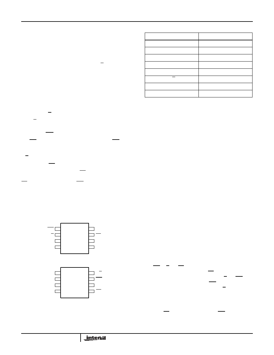
Pin Descriptions
R
H
/V
H
and R
L
/V
L
The high (R
H
/V
H
) and low (R
L
/V
L
) terminals of the X9313
are equivalent to the fixed terminals of a mechanical
potentiometer. The terminology of R
L
/V
L
and R
H
/V
H
references the relative position of the terminal in relation to
wiper movement direction selected by the U/D input and not
the voltage potential on the terminal.
R
W
/V
W
R
W
/V
w
is the wiper terminal and is equivalent to the movable
terminal of a mechanical potentiometer. The position of the
wiper within the array is determined by the control inputs.
The wiper terminal series resistance is typically 40
at V
CC
= 5V.
Up/Down (U/D)
The U/D input controls the direction of the wiper movement
and whether the counter is incremented or decremented.
Increment (INC)
The INC input is negative-edge triggered. Toggling INC will
move the wiper and either increment or decrement the
counter in the direction indicated by the logic level on the
U/D input.
Chip Select (CS)
The device is selected when the CS input is LOW. The
current counter value is stored in nonvolatile memory when
CS is returned HIGH while the INC input is also HIGH. After
the store operation is complete the X9313 will be placed in
the low power standby mode until the device is selected
once again.
Pin Configuration
Principles of Operation
There are three sections of the X9313: the input control,
counter and decode section; the nonvolatile memory; and
the resistor array. The input control section operates just like
an up/down counter. The output of this counter is decoded to
turn on a single electronic switch connecting a point on the
resistor array to the wiper output. Under the proper
conditions the contents of the counter can be stored in
nonvolatile memory and retained for future use. The resistor
array is comprised of 31 individual resistors connected in
series. At either end of the array and between each resistor
is an electronic switch that transfers the potential at that
point to the wiper.
The wiper, when at either fixed terminal, acts like its
mechanical equivalent and does not move beyond the last
position. That is, the counter does not wrap around when
clocked to either extreme.
The electronic switches on the device operate in a "make
before break" mode when the wiper changes tap positions. If
the wiper is moved several positions, multiple taps are
connected to the wiper for t
IW
(INC to V
W
change). The
R
TOTAL
value for the device can temporarily be reduced by
a significant amount if the wiper is moved several positions.
When the device is powered-down, the last wiper position
stored will be maintained in the nonvolatile memory. When
power is restored, the contents of the memory are recalled
and the wiper is set to the value last stored.
Instructions and Programming
The INC, U/D and CS inputs control the movement of the
wiper along the resistor array. With CS set LOW the device
is selected and enabled to respond to the U/D and INC
inputs. HIGH to LOW transitions on INC will increment or
decrement (depending on the state of the U/D input) a seven
bit counter. The output of this counter is decoded to select
one of thirty two wiper positions along the resistive array.
The value of the counter is stored in nonvolatile memory
whenever CS transitions HIGH while the INC input is also
HIGH.
V
CC
CS
INC
U/D
R
H
/V
H
V
SS
1
2
3
4
8
7
6
5
X9313
8-Lead DIP/SOIC
R
L
/V
L
R
W
/V
W
V
CC
CS
U/D
R
H
/V
H
1
2
3
4
8
7
6
5
X9313
8-Lead MSOP
R
L
/V
L
R
W
/V
W
INC
V
SS
TABLE 1. PIN NAMES
SYMBOL
DESCRIPTION
R
H
/V
H
High terminal
R
W
/V
W
Wiper terminal
RL/VL
Low terminal
V
SS
Ground
V
CC
Supply voltage
U/D
Up/Down control input
INC
Increment control input
CS
Chip Select control input
X9313
5
FN8177.2
September 9, 2005
The system may select the X9313, move the wiper and
deselect the device without having to store the latest wiper
position in nonvolatile memory. After the wiper movement is
performed as described above and once the new position is
reached, the system must keep INC LOW while taking CS
HIGH. The new wiper position will be maintained until
changed by the system or until a power-up/down cycle
recalled the previously stored data.
This procedure allows the system to always power-up to a
preset value stored in nonvolatile memory; then during
system operation minor adjustments could be made. The
adjustments might be based on user preference, system
parameter changes due to temperature drift, etc.
The state of U/D may be changed while CS remains LOW.
This allows the host system to enable the device and then
move the wiper up and down until the proper trim is attained.
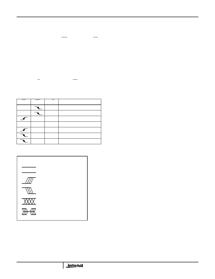
Symbol Table
TABLE 2. MODE SELECTION
CS
INC
U/D
MODE
L
H
Wiper up
L
L
Wiper down
H
X
Store wiper position
H
X
X
Standby current
L
X
No store, return to standby
L
H
Wiper up (not recommended)
L
L
Wiper down (not recommended)
WAVEFORM
INPUTS
OUTPUTS
Must be
steady
Will be
steady
May change
from Low to
High
Will change
from Low to
High
May change
from High to
Low
Will change
from High to
Low
Don't Care:
Changes
Allowed
Changing:
State Not
Known
N/A
Center Line
is High
Impedance
X9313