1
Æ
FN8180.0
CAUTION: These devices are sensitive to electrostatic discharge; follow proper IC Handling Procedures.
1-888-INTERSIL or 321-724-7143
|
Intersil (and design) is a registered trademark of Intersil Americas Inc.
XDCP is a trademark of Intersil Americas Inc. Copyright Intersil Americas Inc. 2004. All Rights Reserved
All other trademarks mentioned are the property of their respective owners.
X93154
Low Noise, Low Power, 32 Taps
Digitally Controlled Potentiometer
(XDCPTM)
The Intersil X93154 is a digitally controlled potentiometer
(XDCP). The device consists of a resistor array, wiper
switches, a control section, and nonvolatile memory. The
wiper position is controlled by a 3-wire interface.
The potentiometer is implemented by a resistor array
composed of 31 resistive elements and a wiper switching
network. The position of the wiper element is controlled by
the CS, U/D, and INC inputs. The position of the wiper can
be stored in nonvolatile memory and then be recalled upon a
subsequent power-up operation.
The device is connected as a two-terminal variable resistor
and can be used in a wide variety of applications including:
- Bias and Gain Control
- LCD Contrast Adjustment
Features
∑ Solid-State Potentiometer
∑ 3-Wire Serial Interface
∑ 32 Wiper Tap Points
- Wiper position stored in nonvolatile memory and
recalled on power-up
∑ 31 Resistive Elements
- Temperature compensated
- Maximum resistance tolerance of ±30%
- Terminal voltage, 0 to V
CC
∑ Low Power CMOS
- V
CC
= 3V±10%
- Active current, 250µA max.
- Standby current, 1µA max.
∑ High Reliability
- Endurance 200,000 data changes per bit
- Register data retention, 100 years
∑ R
TOTAL
Value = 50k
∑ Packages
- 8-lead MSOP, TDFN
- Pb-free available (RoHS compliant)
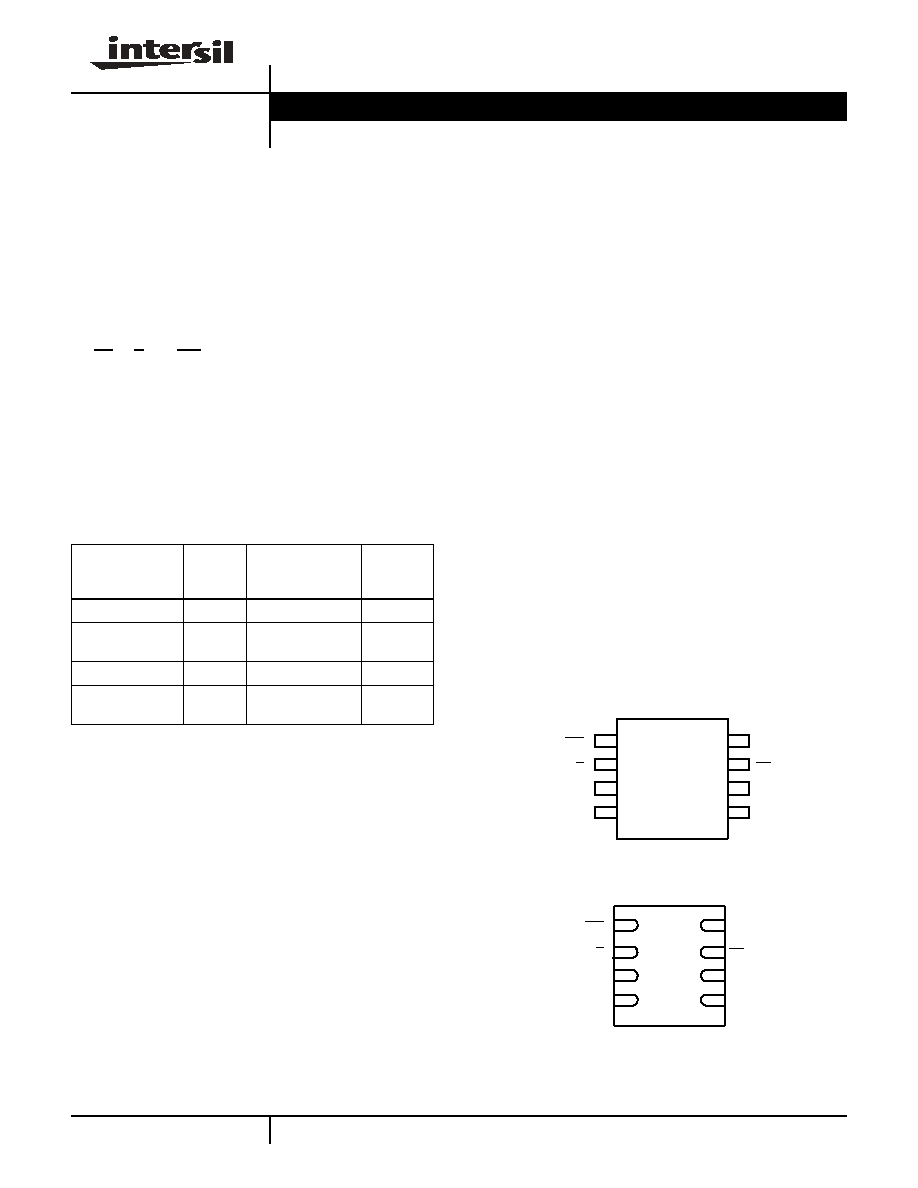
Pinouts
X93154
(8 LD MSOP)
TOP VIEW
X93154
(8 LD TDFN)
TOP VIEW
1
NC can be left unconnected, or connected to any voltage between V
SS
and V
CC
Ordering Information
ORDERING
NUMBER
RTOTAL
PACKAGE
TEMP
RANGE
(∞C)
X93154UU8I-3
50k
8 Ld TDFN
-40 to +85
X93154UU8IZ-3
(See Note)
50k
8 Ld TDFN
(Pb-free)
-40 to +85
X93154UM8I-3
50k
8 Ld MSOP
-40 to +85
X93154UM8IZ-3
(See Note)
50k
8 Ld MSOP
(Pb-free)
-40 to +85
NOTE: Intersil Pb-free products employ special Pb-free material sets;
molding compounds/die attach materials and 100% matte tin plate
termination finish, which are RoHS compliant and compatible with
both SnPb and Pb-free soldering operations. Intersil Pb-free products
are MSL classified at Pb-free peak reflow temperatures that meet or
exceed the Pb-free requirements of IPC/JEDEC J STD-020.
V
CC
CS
INC
U/D
R
H
V
SS
1
2
3
4
8
7
6
5
R
L
NC
1
V
CC
CS
INC
U/D
R
H
V
SS
R
L
NC
1
**Contact factory for TDFN ordering info.
1
2
3
4
8
7
6
5
Data Sheet
December 22, 2004
2
FN8180.0
December 22, 2004
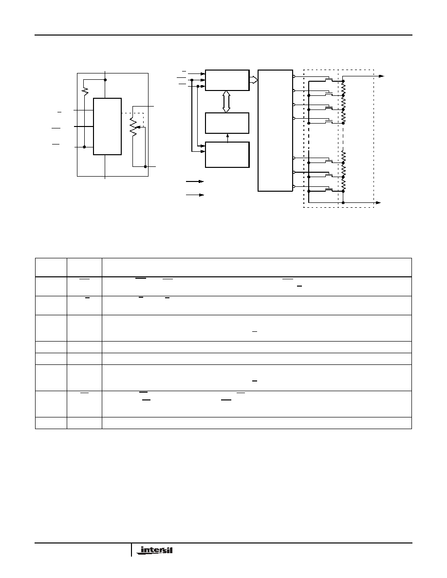
Block Diagram
5-Bit
Up/Down
Counter
5-Bit
Nonvolatile
Memory
Store and
Recall
Control
Circuitry
One
of
Decoder
Resistor
Array
R
H
U/D
INC
CS
Transfer
Gates
Thirty
V
CC
V
SS
R
L
Control
and
Memory
Up/Down
(U/D)
Increment
(INC)
Device Select
(CS)
V
CC
(Supply Voltage)
V
SS
(Ground)
R
H
General
Detailed
0
1
2
28
29
30
31
Two
R
L
30K
Pin Descriptions
MSOP
TDFN
SYMBOL
BRIEF DESCRIPTION
1
INC
Increment (INC). The INC input is negative-edge triggered. Toggling INC will move the wiper and either increment or
decrement the counter in the direction indicated by the logic level on the U/D input.
2
U/D
Up/Down (U/D). The U/D input controls the direction of the wiper movement and whether the counter is incremented or
decremented.
3
R
H
R
H
. The R
H
and R
L
pins of the X93154 are equivalent to the fixed terminals of a mechanical potentiometer. The minimum
voltage is VSS and the maximum is VCC. The terminology of R
H
and R
L
references the relative position of the terminal
in relation to wiper movement direction selected by the U/D input.
4
V
SS
Ground.
5
NC
No Connection. (or can be connected to any voltage between V
SS
and V
CC
.)
6
R
L
R
L
. The R
H
and R
L
pins of the X93154 are equivalent to the fixed terminals of a mechanical potentiometer. The minimum
voltage is VSS and the maximum is VCC. The terminology of R
H
and R
L
references the relative position of the terminal
in relation to wiper movement direction selected by the U/D input.
7
CS
Chip Select (CS). The device is selected when the CS input is LOW. The current counter value is stored in nonvolatile
memory when CS is returned HIGH while the INC input is also HIGH. After the store operation is complete, the X93154
will be placed in the low power standby mode until the device is selected once again.
8
V
CC
Supply Voltage.
X93154
3
FN8180.0
December 22, 2004
Absolute Maximum Ratings
Recommended Operating Conditions
Temperature under bias . . . . . . . . . . . . . . . . . . . . . .-65
∞C to +135∞C
Storage temperature . . . . . . . . . . . . . . . . . . . . . . . .-65∞C to +150∞C
Voltage on CS, INC, U/D, R
H
, R
L
and V
CC
with respect to V
SS
. . . . . . . . . . . . . . . . . . . . . . . . . . -1V to +6.5V
Lead temperature (soldering 10 seconds) . . . . . . . . . . . . . . . . 300∞C
Maximum resistor current . . . . . . . . . . . . . . . . . . . . . . . . . . . . . 2mA
Temperature Range
Industrial. . . . . . . . . . . . . . . . . . . . . . . . . . . . . . . . .-40∞C to +85∞C
Supply Voltage
V
CC
. . . . . . . . . . . . . . . . . . . . . . . . . . . . . . . . . . . . . . .3V ±10%
(8)
CAUTION: Stresses above those listed in "Absolute Maximum Ratings" may cause permanent damage to the device. This is a stress only rating and operation of the
device at these or any other conditions above those indicated in the operational sections of this specification is not implied.
Potentiometer Specifications
Over recommended operating conditions unless otherwise stated.
SYMBOL
PARAMETER
TEST CONDITIONS/NOTES
MIN
TYP
MAX
UNIT
R
TOT
End to end resistance
35
50
65
k
V
R
R
H
, R
L
terminal voltages
0
V
CC
V
Power rating
R
TOTAL
= 50k
1
mW
(7)
Noise
Ref: 1kHz
-120
dBV
(7)
R
W
Wiper Resistance
(5) (6)
1000
I
W
Wiper Current
(5) (6)
0.6
mA
Resolution
3
%
Absolute linearity
(1)
V
H(n)(actual)
-V
H(n)(expected)
±1
MI
(3)
Relative linearity
(2)
V
H(n+1)
-[V
H(n)+MI
]
±0.5
MI
(3)
R
TOTAL
temperature coefficient
(7)
±35
ppm/∞C
C
H
/C
L
/C
W
Potentiometer capacitances
See circuit #3
10/10/25
pF
(7)
NOTES:
1. Absolute linearity is utilized to determine actual wiper voltage versus expected voltage = (V
H(n)
(actual)-V
H(n)
(expected)) = ±1 Ml Maximum. n =
1 .. 29 only
2. Relative linearity is a measure of the error in step size between taps = V
H(n+1)
--[V
H(n)
+ Ml] = ±0.5 Ml, n = 1 .. 29 only.
3. 1 Ml = Minimum Increment = R
TOT
/31.
4. Typical values are for T
A
= 25∞C and nominal supply voltage.
5. This parameter is periodically sampled and not 100% tested
6. Typical values are for T
A
= 25∞C and nominal supply voltage.
7. This parameter is not 100% tested.
8. When performing multiple write operations, V
CC
must not decrease by more than 150mV from its initial value.
DC Electrical Specifications
Over recommended operating conditions unless otherwise specified.
SYMBOL
PARAMETER
TEST CONDITIONS
MIN
TYP(4)
MAX
UNIT
I
CC1
VCC active current (Increment)
CS = V
IL
, U/D = V
IL
or V
IH
and INC = 0.4V @
max. t
CYC
50
250
µA
I
CC2
VCC active current (Store)
(EEPROM Store)
CS = V
IH
, U/D = V
IL
or V
IH
and INC = V
IH
@
max. t
WR
600
µA
I
SB
Standby supply current
CS = V
CC
- 0.3V, U/D and INC = V
SS
or
V
CC
- 0.3V
1
µA
I
LI
CS
V
IN
= V
CC
±1
µA
I
LI
CS
V
CC
= 3V, CS = 0
60
100
150
µA
I
LI
INC, U/D input leakage current
V
IN
= V
SS
to V
CC
±1
µA
V
IH
CS, INC, U/D input HIGH voltage
V
CC
x 0.7
V
CC
+ 0.5
V
V
IL
CS, INC, U/D input LOW voltage
-0.5
V
CC
x 0.1
V
C
IN
(5)(7)
CS, INC, U/D input capacitance
V
CC
= 3V, V
IN
= V
SS
, T
A
= 25∞C, f = 1MHz
10
pF
X93154

4
FN8180.0
December 22, 2004
Test Circuit #1
Circuit #2 SPICE Macro Model
Power Up and Down Requirements
There are no restrictions on the power-up or power-down
conditions of V
CC
and the voltages applied to the
potentiometer pins provided that V
CC
is always more
positive than or equal to V
H
and V
L
, i.e., V
CC
V
H,
V
L
. The
V
CC
ramp rate spec is always in effect.
A.C. Timing
Endurance and Data Retention
PARAMETER
MIN
UNIT
Minimum endurance
200,000
Data changes per bit
Data retention
100
Years
V
L
Test Point
V
H
/R
H
A.C. Conditions of Test
Input pulse levels
0V to 3V
Input rise and fall times
10ns
Input reference levels
1.5V
C
H
C
L
10pF
10pF
R
H
R
TOTAL
C
W
25pF
R
L
AC Electrical Specifications
Over recommended operating conditions unless otherwise specified.
SYMBOL
PARAMETER
MIN
TYP(6)
MAX
UNIT
t
Cl
CS to INC setup
100
ns
t
lD
INC HIGH to U/D change
100
ns
t
DI
U/D to INC setup
100
ns
t
lL
INC LOW period
1
µs
t
lH
INC HIGH period
1
µs
t
lC
INC Inactive to CS inactive
1
µs
t
CPH
CS Deselect time (NO STORE)
250
ns
t
CPH
CS Deselect time (STORE)
10
ms
t
CYC
INC cycle time
2
µs
t
R
, t
F
(7)
INC input rise and fall time
500
µs
t
R
V
CC
(7)
VCC power-up rate
1.0
10,000
V/ms
t
WR
Store cycle
5
10
ms
CS
INC
U/D
t
CI
t
IL
t
IH
t
CYC
t
ID
t
DI
t
IC
t
CPH
t
F
t
R
10%
90%
90%
(Store)
X93154
5
FN8180.0
December 22, 2004
Pin Descriptions
R
H
and R
L
The R
H
and R
L
pins of the X93154 are equivalent to the
fixed terminals of a mechanical potentiometer. The minimum
voltage is V
SS
and the maximum is V
CC
. The terminology of
R
H
and R
L
references the relative position of the terminal in
relation to wiper movement direction selected by the U/D
input.
Up/Down (U/D)
The U/D input controls the direction of the wiper movement
and whether the counter is incremented or decremented.
Increment (INC)
The INC input is negative-edge triggered. Toggling INC will
move the wiper and either increment or decrement the
counter in the direction indicated by the logic level on the
U/D input.
Chip Select (CS)
The device is selected when the CS input is LOW. The
current counter value is stored in nonvolatile memory when
CS is returned HIGH while the INC input is also HIGH. After
the store operation is complete the X93154 will be placed in
the low power standby mode until the device is selected
once again.
Pin Configuration
Principles of Operation
There are three sections of the X93154: the input control,
counter and decode section; the nonvolatile memory; and
the resistor array. The input control section operates just like
an up/down counter. The output of this counter is decoded to
turn on a single electronic switch connecting a point on the
resistor array to the wiper output. Under the proper
conditions the contents of the counter can be stored in
nonvolatile memory and retained for future use. The resistor
array is comprised of 31 individual resistors connected in
series. At either end of the array and between each resistor
is an electronic switch that transfers the connection at that
point to the wiper.
The wiper, when at either fixed terminal, acts like its
mechanical equivalent and does not move beyond the last
position. That is, the counter does not wrap around when
clocked to either extreme.
If the wiper is moved several positions, multiple taps are
connected to the wiper for t
IW
(INC to V
W
change). The 2-
terminal resistance value for the device can temporarily
change by a significant amount if the wiper is moved several
positions.
When the device is powered-down, the last wiper position
stored will be maintained in the nonvolatile memory. When
power is restored, the contents of the memory are recalled
and the wiper is set to the value last stored.
Instructions and Programming
The INC, U/D and CS inputs control the movement of the
wiper along the resistor array. With CS set LOW the device
is selected and enabled to respond to the U/D and INC
inputs. HIGH to LOW transitions on INC will increment or
decrement (depending on the state of the U/D input) a five
bit counter. The output of this counter is decoded to select
one of thirty two wiper positions along the resistive array.
The value of the counter is stored in nonvolatile memory
whenever CS transitions HIGH while the INC input is also
HIGH. In order to avoid an accidental store during power-up,
CS must go HIGH with V
CC
during initial power-up. When
performing multiple write operations, V
CC
must not decrease
by more than 150mV from its initial value. When left open,
the CS pin is internally pulled up to V
CC
by an internal 30k
resistor.
The system may select the X93154, move the wiper and
deselect the device without having to store the latest wiper
position in nonvolatile memory. After the wiper movement is
performed as described above and once the new position is
reached, the system must keep INC LOW while taking CS
HIGH. The new wiper position will be maintained until
changed by the system or until a power-up/down cycle
recalled the previously stored data. In order to recall the
stored position of the wiper on power-up, the CS pin must be
held HIGH.
Pin Names
SYMBOL
DESCRIPTION
RH
High terminal
RL
Low terminal
VSS
Ground
VCC
Supply voltage
U/D
Up/Down control input
INC
Increment control input
CS
Chip Select control input
V
CC
CS
INC
U/D
R
H
/V
H
V
SS
1
2
3
4
8
7
6
5
X93154
MSOP
R
L
/V
L
NC*
*NC = No Connect. Can be connected to any
voltage between V
SS
and V
CC
, or left unconnected.
X93154
6
FN8180.0
December 22, 2004
This procedure allows the system to always power-up to a
preset value stored in nonvolatile memory; then during
system operation minor adjustments could be made. The
adjustments might be based on user preference, system
parameter changes due to temperature drift, or other system
trim requirements.
The state of U/D may be changed while CS remains LOW.
This allows the host system to enable the device and then
move the wiper up and down until the proper trim is attained.
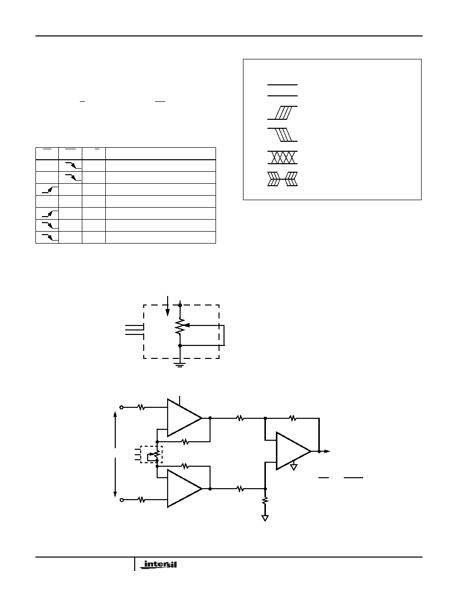
Symbol Table
Applications Information
Electronic digitally controlled (XDCP) potentiometers provide
three powerful application advantages; (1) the variability and
reliability of a solid-state potentiometer (2) the flexibility of
computer-based digital controls, and (3) the retentivity of
nonvolatile memory used for the storage of multiple
potentiometer settings or data.
Low Voltage High Impedance Instrumentation Amplifier
Mode Selection
CS
INC
U/D
MODE
L
H
Wiper Up
L
L
Wiper Down
H
X
Store Wiper Position
H
X
X
Standby Current
L
X
No Store, Return to Standby
L
H
Wiper Up (not recommended)
L
L
Wiper Down (not recommended)
WAVEFORM
INPUTS
OUTPUTS
Must be
steady
Will be
steady
May change
from Low to
High
Will change
from Low to
High
May change
from High to
Low
Will change
from High to
Low
Don't Care:
Changes
Allowed
Changing:
State Not
Known
N/A
Center Line
is High
Impedance
V
R
Two terminal variable resistor.
variable current
I
+
-
U1A
10K
50K
-
+
U1C
Gain =
50K
10K
1 +
50K
R
TOTAL
)
(
U1 = LT1467
V
OUT
50k
-
+
U1B
10K
50K
50K
X93154 (R
TOTAL
)
10K
+
10K
-
V
IN
3.3V
X93154
7
FN8180.0
December 22, 2004
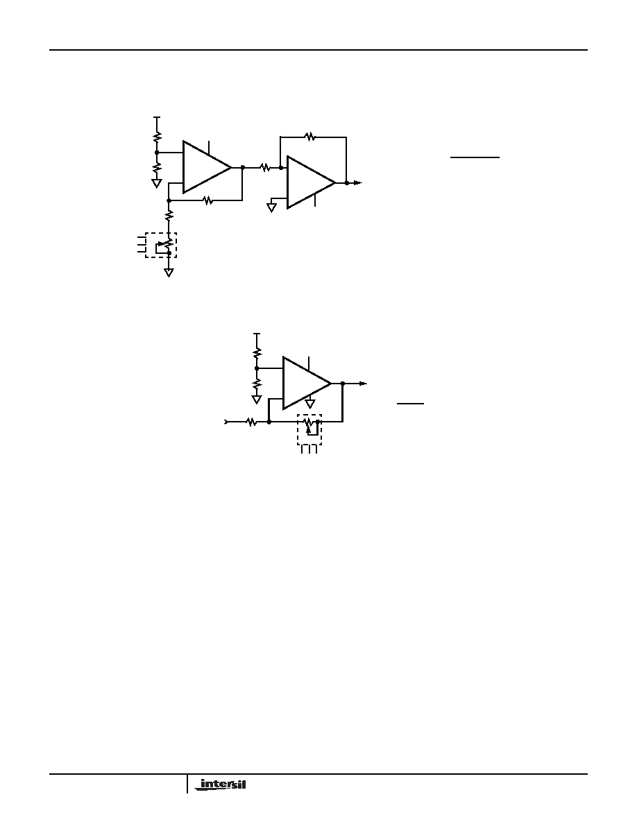
Applications Information (Continued)
Micro-Power LCD Contrast Control
Single Supply Variable Gain Amplifier
+
-
U1A
100K
300K
-
+
U1B
1 +
100K
50K + R
TOTAL
)
(
U1 = LMC6042
V
OUT
= -3.88
-12V
100K
X93154 (R
TOTAL
)
240K
3.3V
100K
3.3V
50K
V
OUT
= -2.75V to -11.6V
Gain =
R
TOTAL
10K
+
-
U1
20K
3.3V
20K
3.3V
V
OUT
U1 = LMC6042
10K
V
IN
X93154
(R
TOTAL
)
X93154

8
FN8180.0
December 22, 2004
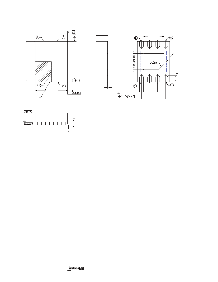
MSOP Packaging Information
0.118 ± 0.002
(3.00 ± 0.05)
0.040 ± 0.002
(1.02 ± 0.05)
0.150 (3.81)
Ref.
0.193 (4.90)
0.030 (0.76)
0.036 (0.91)
0.032 (0.81)
0.007 (0.18)
0.005 (0.13)
0.008 (0.20)
0.004 (0.10)
0.0216 (0.55)
7∞ Typ.
R 0.014 (0.36)
0.118 ± 0.002
(3.00 ± 0.05)
0.012 + 0.006 / -0.002
(0.30 + 0.15 / -0.05)
0.0256 (0.65) Typ.
8-Lead Miniature Small Outline Gull Wing Package Type M
NOTE:
1. ALL DIMENSIONS IN INCHES AND (MILLIMETERS)
0.220"
0.0256" Typical
0.025"
Typical
0.020"
Typical
8 Places
FOOTPRINT
Ref.
X93154
9
All Intersil U.S. products are manufactured, assembled and tested utilizing ISO9000 quality systems.
Intersil Corporation's quality certifications can be viewed at www.intersil.com/design/quality
Intersil products are sold by description only. Intersil Corporation reserves the right to make changes in circuit design, software and/or specifications at any time without
notice. Accordingly, the reader is cautioned to verify that data sheets are current before placing orders. Information furnished by Intersil is believed to be accurate and
reliable. However, no responsibility is assumed by Intersil or its subsidiaries for its use; nor for any infringements of patents or other rights of third parties which may result
from its use. No license is granted by implication or otherwise under any patent or patent rights of Intersil or its subsidiaries.
For information regarding Intersil Corporation and its products, see www.intersil.com
FN8180.0
December 22, 2004
TDFN Packaging Information
0.75±0.05
1.30±0.10
1.50 Ref. (2X)
0.25±0.05 (8X)
0.40±0.10
DAP Size 1.6 x 1.3
0.50 Typ. (6X)
2.00±0.10
(S)
0.20 Ref.
0.0≠0.05
Pin 1 Index Area
2.50±
0.10
(S)
X93154