1
Æ
FN8183.1
CAUTION: These devices are sensitive to electrostatic discharge; follow proper IC Handling Procedures.
1-888-INTERSIL or 1-888-468-3774
|
Intersil (and design) is a registered trademark of Intersil Americas Inc.
XDCP is a trademark of Intersil Americas, Inc. Copyright Intersil Americas Inc. 2004, 2005. All Rights Reserved
All other trademarks mentioned are the property of their respective owners.
X9317
Low Noise, Low Power, 100 Taps
Digitally Controlled Potentiometer
(XDCPTM)
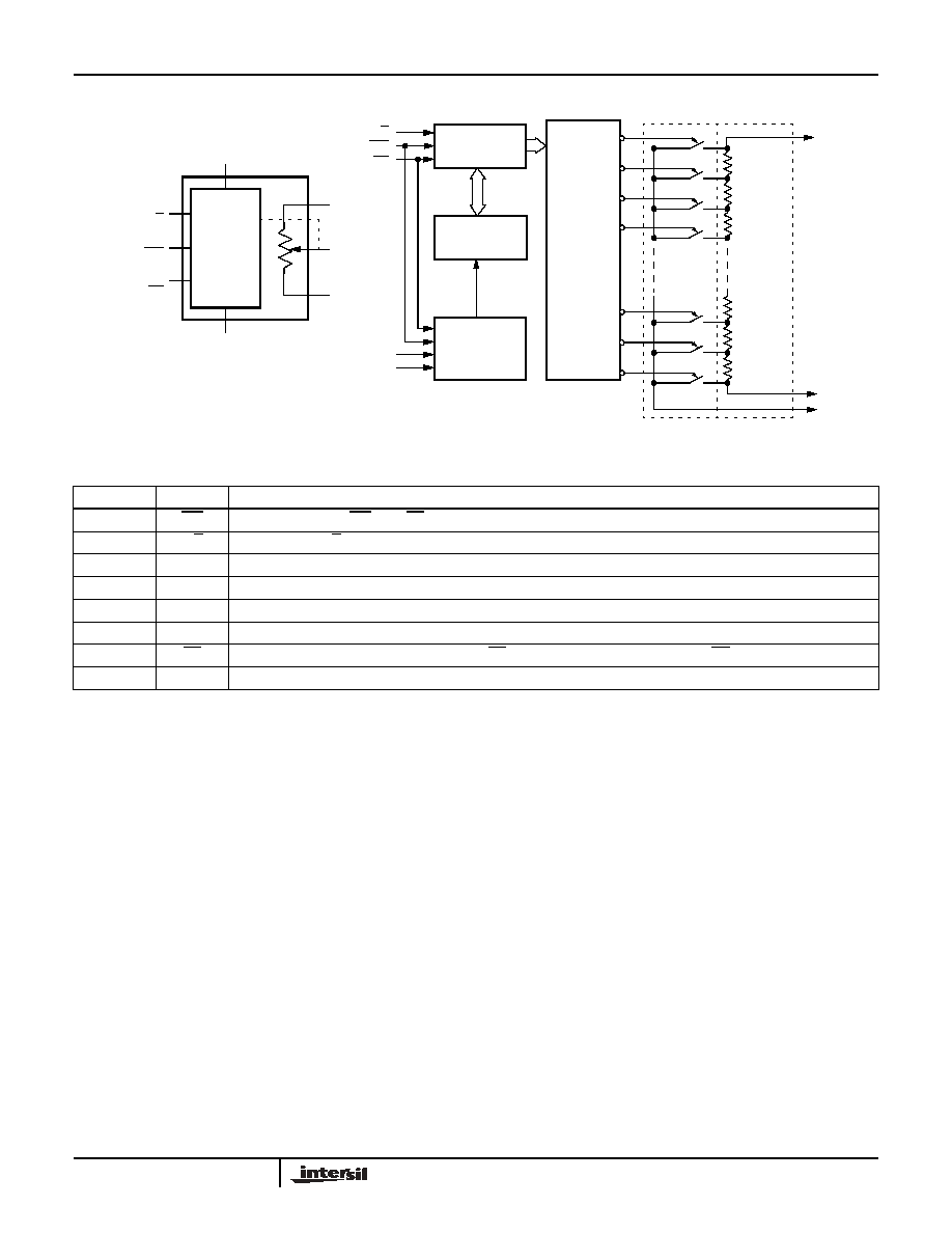
The Intersil X9317 is a digitally controlled potentiometer
(XDCP). The device consists of a resistor array, wiper
switches, a control section, and nonvolatile memory. The
wiper position is controlled by a 3-wire interface.
The potentiometer is implemented by a resistor array
composed of 99 resistive elements and a wiper switching
network. Between each element and at either end are tap
points accessible to the wiper terminal. The position of the
wiper element is controlled by the CS, U/D, and INC inputs.
The position of the wiper can be stored in nonvolatile
memory and then be recalled upon a subsequent power-up
operation.
The device can be used as a three-terminal potentiometer
for voltage control or as a two-terminal variable resistor for
current control in a wide variety of applications.
Features
∑ Solid-State Potentiometer
∑ 3-Wire Serial Up/Down Interface
∑ 100 Wiper Tap Points
- Wiper position stored in nonvolatile memory and
recalled on power-up
∑ 99 Resistive Elements
- Temperature compensated
- End to end resistance range ±20%
∑ Low Power CMOS
- V
CC
= 2.7V to 5.5V, and 5V ±10%
- Standby current < 1µA
∑ High Reliability
- Endurance, 100,000 data changes per bit
- Register data retention, 100 years
∑ R
TOTAL
Values = 1k
, 10k, 50k, 100k
∑ Packages
- 8 Ld SOIC, DIP, TSSOP, and MSOP
∑ Pb-Free Plus Anneal Available (RoHS Compliant)
Applications
∑ LCD Bias Control
∑ DC Bias Adjustment
∑ Gain and Offset Trim
∑ Laser Diode Bias Control
∑ Voltage Regulator Output Control
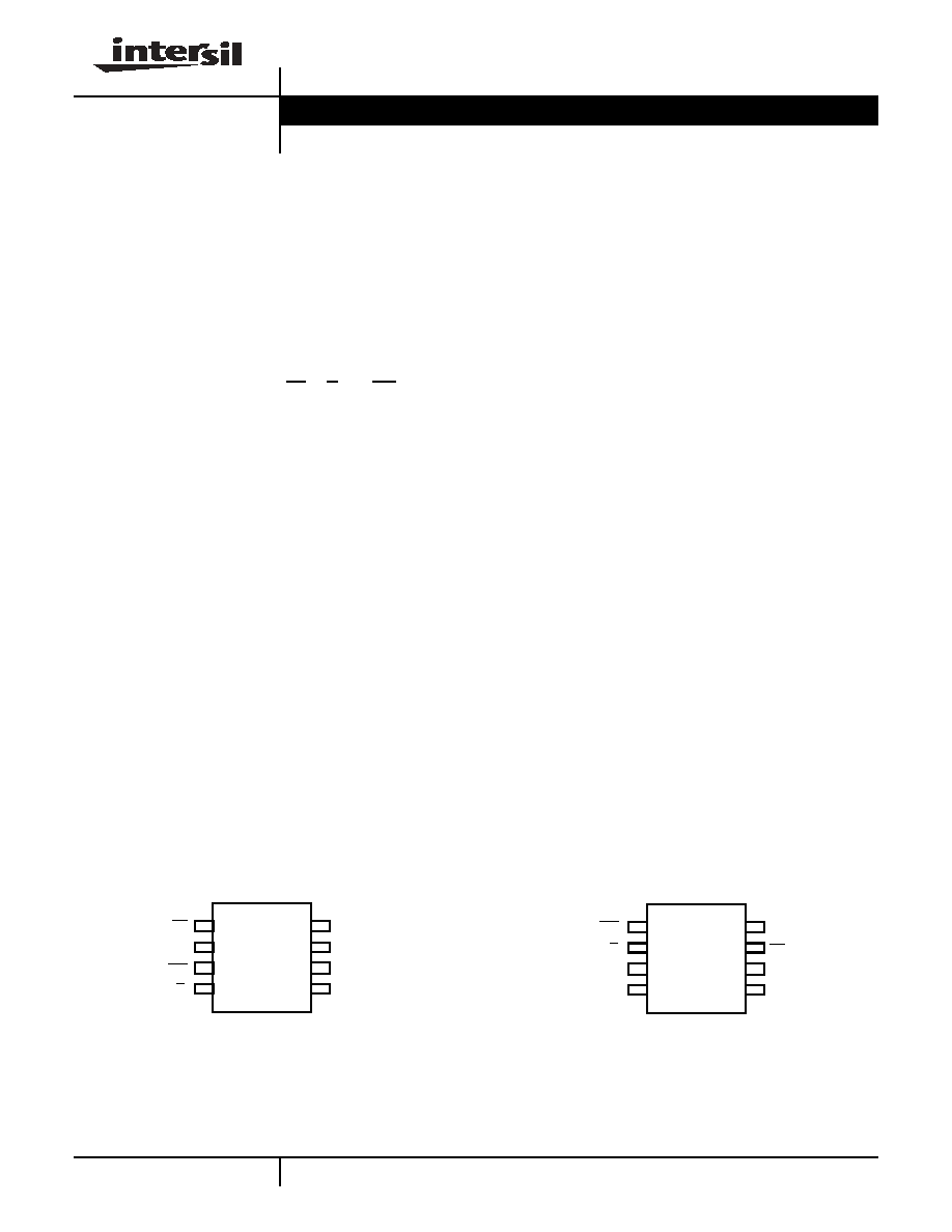
Pinouts
X9317
(8 LD TSSOP)
TOP VIEW
X9317
(8 LD DIP, 8 LD SOIC, 8 LD MSOP)
TOP VIEW
INC
R
L
/V
L
CS
V
CC
1
2
3
4
8
7
6
5
X9317
U/D
R
W
/V
W
V
SS
R
H
/V
H
R
H
V
CC
INC
U/D
1
2
3
4
8
7
6
5
X9317
V
SS
CS
R
L
R
W
Data Sheet
September 9, 2005
5
FN8183.1
September 9, 2005
Block Diagram
Up/Down
Counter
7-Bit
Nonvolatile
Memory
Store and
Recall
Control
Circuitry
One
of
One
Decoder
Resistor
Array
R
H
U/D
INC
CS
Wiper
Switches
Hundred
V
CC
V
SS
R
L
R
W
Control
and
Memory
Up/Down
(U/D)
Increment
(INC)
Device Select
(CS)
V
CC
(Supply Voltage)
V
SS
(Ground)
R
H
R
W
R
L
General
Detailed
0
1
2
96
97
98
99
Pin Descriptions
DIP/SOIC
SYMBOL
BRIEF DESCRIPTION
1
INC
Increment. Toggling INC while CS is low moves the wiper either up or down.
2
U/D
Up/Down. The U/D input controls the direction of the wiper movement.
3
R
H
The high terminal is equivalent to one of the fixed terminals of a mechanical potentiometer.
4
V
SS
Ground.
5
R
W
The wiper terminal is equivalent to the movable terminal of a mechanical potentiometer.
6
R
L
The low terminal is equivalent to one of the fixed terminals of a mechanical potentiometer.
7
CS
Chip Select. The device is selected when the CS input is LOW, and de-selected when CS is high.
8
V
CC
Supply Voltage.
X9317