1
Æ
FN8196.1
CAUTION: These devices are sensitive to electrostatic discharge; follow proper IC Handling Procedures.
1-888-INTERSIL or 1-888-468-3774
|
Intersil (and design) is a registered trademark of Intersil Americas Inc.
XDCP is a trademark of Intersil Americas Inc. Copyright Intersil Americas Inc. 2005. All Rights Reserved
All other trademarks mentioned are the property of their respective owners.
X9421
Low Noise/Low Power/SPI Bus
Single Digitally Controlled (XDCPTM)
Potentiometer
FEATURES
∑ Single Voltage Potentiometer
∑ 64 Resistor Taps
∑ SPI Serial Interface for Write, Read, and Transfer
Operations of the Potentiometer
∑ Wiper Resistance, 150
Typical at 5V
∑ 4 Non-Volatile Data Registers
∑ Non-Volatile Storage of Multiple Wiper Positions
∑ Power-on Recall. Loads Saved Wiper Position
on Power-up.
∑ Standby Current < 5µA Max
∑ V
CC
: 2.7V to 5.5V Operation
∑ 2.5k
, 10k
End to End Resistance
∑ 100 yr. Data Retention
∑ Endurance: 100, 000 Data Changes per Bit per
Register
∑ 14 Ld TSSOP, 16 Ld SOIC
∑ Low Power CMOS
∑ Pb-Free Plus Anneal Available (RoHS Compliant)
DESCRIPTION
The X9421 integrates a single digitally controlled
potentiometer (XDCP) on a monolithic CMOS
integrated circuit.
The digital controlled potentiometer is implemented
using 63 resistive elements in a series array. Between
each element are tap points connected to the wiper
terminal through switches. The position of the wiper on
the array is controlled by the user through the SPI bus
interface. The potentiometer has associated with it a
volatile Wiper Counter Register (WCR) and a four non-
volatile Data Registers that can be directly written to
and read by the user. The contents of the WCR
controls the position of the wiper on the resistor array
though the switches. Powerup recalls the contents of
the default data register (DR0) to the WCR.
The XDCP can be used as a three-terminal
potentiometer or as a two terminal variable resistor in
a wide variety of applications including control,
parameter adjustments, and signal processing.
BLOCK DIAGRAM
64-taps
10k
inc / dec
R
H
/V
H
R
L
/V
L
R
W
/V
W
POT
V
CC
V
SS
SPI
bus
address
data
status
write
read
wiper
transfer
Power-on Recall
Wiper Counter
Register (WCR)
Data Registers
4 Bytes
control
interface
Bus
Interface &
Control
Data Sheet
September 23, 2005
2
FN8196.1
September 23, 2005
Ordering Information
PART NUMBER
PART MARKING V
CC
LIMITS (V)
POTENTIOMETER
ORGANIZATION
(k
)
TEMP RANGE (∞C)
PACKAGE
X9421YS16*
X9421YS
5 ±10%
2.5
0 to 70
16 Ld SOIC (300 mil)
X9421YS16Z* (Note)
X9421YS Z
0 to 70
16 Ld SOIC (300 mil) (Pb-free)
X9421YS16I*
-40 to 85
16 Ld SOIC (300 mil)
X9421YS16IZ* (Note)
X9421YS Z I
-40 to 85
16 Ld SOIC (300 mil) (Pb-free)
X9421YV14*
0 to 70
14 Ld TSSOP (4.4mm)
X9421YV14I*
-40 to 85
14 Ld TSSOP (4.4mm)
X9421WS16*
X9421WS
10
0 to 70
16 Ld SOIC (300 mil)
X9421WS16Z* (Note)
X9421WS Z
0 to 70
16 Ld SOIC (300 mil) (Pb-free)
X9421WS16I*
X9421WS I
-40 to 85
16 Ld SOIC (300 mil)
X9421WS16IZ* (Note)
X9421WS Z I
-40 to 85
16 Ld SOIC (300 mil) (Pb-free)
X9421WV14*
X9421WV
0 to 70
14 Ld TSSOP (4.4mm)
X9421WV14I*
X9421WV I
-40 to 85
14 Ld TSSOP (4.4mm)
X9421YS16-2.7*
2.7 to 5.5
2.5
0 to 70
16 Ld SOIC (300 mil)
X9421YS16Z-2.7* (Note)
X9421YS Z F
0 to 70
16 Ld SOIC (300 mil) (Pb-free)
X9421YS16I-2.7*
-40 to 85
16 Ld SOIC (300 mil)
X9421YS16IZ-2.7* (Note)
X9421YS Z G
-40 to 85
16 Ld SOIC (300 mil) (Pb-free)
X9421YV14-2.7*
0 to 70
14 Ld TSSOP (4.4mm)
X9421YV14I-2.7*
X9421YV G
-40 to 85
14 Ld TSSOP (4.4mm)
X9421WS16-2.7*
X9421WS F
10
0 to 70
16 Ld SOIC (300 mil)
X9421WS16Z-2.7* (Note)
X9421WS Z F
0 to 70
16 Ld SOIC (300 mil) (Pb-free)
X9421WS16I-2.7*
X9421WS G
-40 to 85
16 Ld SOIC (300 mil)
X9421WS16IZ-2.7* (Note)
X9421WS Z G
-40 to 85
16 Ld SOIC (300 mil) (Pb-free)
X9421WV14-2.7*
X9421WV F
0 to 70
14 Ld TSSOP (4.4mm)
X9421WV14I-2.7*
X9421WV G
-40 to 85
14 Ld TSSOP (4.4mm)
*Add "T1" suffix for tape and reel.
NOTE: Intersil Pb-free plus anneal products employ special Pb-free material sets; molding compounds/die attach materials and 100% matte tin plate
termination finish, which are RoHS compliant and compatible with both SnPb and Pb-free soldering operations. Intersil Pb-free products are MSL
classified at Pb-free peak reflow temperatures that meet or exceed the Pb-free requirements of IPC/JEDEC J STD-020.
X9421
3
FN8196.1
September 23, 2005
DETAILED FUNCTIONAL DIAGRAM
CIRCUIT LEVEL APPLICATIONS
∑ Vary the gain of a voltage amplifier
∑ Provide programmable dc reference voltages for
comparators and detectors
∑ Control the volume in audio circuits
∑ Trim out the offset voltage error in a voltage
amplifier circuit
∑ Set the output voltage of a voltage regulator
∑ Trim the resistance in Wheatstone bridge circuits
∑ Control the gain, characteristic frequency and
Q-factor in filter circuits
∑ Set the scale factor and zero point in sensor signal
conditioning circuits
∑ Vary the frequency and duty cycle of timer ICs
∑ Vary the dc biasing of a pin diode attenuator in RF
circuits
∑ Provide a control variable (I, V, or R) in feedback
circuits
SYSTEM LEVEL APPLICATIONS
∑ Adjust the contrast in LCD displays
∑ Control the power level of LED transmitters in
communication systems
∑ Set and regulate the DC biasing point in an RF
power amplifier in wireless systems
∑ Control the gain in audio and home entertainment
systems
∑ Provide the variable DC bias for tuners in RF
wireless systems
∑ Set the operating points in temperature control
systems
∑ Control the operating point for sensors in industrial
systems
∑ Trim offset and gain errors in artificial intelligent
systems
WIPER
COUNTER
REGISTER
(WCR)
R
H
/V
H
R
L
/V
L
DATA
R
W
/V
W
INTERF
A
CE
AND
CONTROL
CIRCUITR
Y
V
CC
V
SS
CS
SCK
A0
SO
SI
HOLD
WP
Control
64--taps
10k
Power-on Recall
DR0 DR1
DR2 DR3
X9421
4
FN8196.1
September 23, 2005
PIN CONFIGURATION
PIN ASSIGNMENTS
TSSOP pin
SOIC pin
Symbol
Brief Description
1
2
SO
Serial Data Output
2
3
NC
No Connect
3
NC
No Connect
4
4
CS
Chip Select
5
5
SCK
Serial Clock
6
6
SI
Serial Data Input
7
8
V
SS
System Ground
8
9
WP
Hardware Write Protect
9
10
A0
Device Address
10
11
HOLD
Device select. Pause the serial bus.
11
12
R
W
/ V
W
Wiper Terminal of the Potentiometer.
12
13
R
H
/ V
H
High Terminal of the Potentiometer.
13
14
R
L
/ V
L
Low Terminal of the Potentiometer.
14
16
V
CC
System Supply Voltage
1
NC
No Connect
7
NC
No Connect
15
NC
No Connect
V
CC
R
L
/V
L
VSS
1
2
3
4
5
6
7
8
14
13
12
11
10
9
NC
R
W
/V
W
SCK
CS
TSSOP
R
H
/V
H
X9421
S0
NC
SI
HOLD
WP
A0
1
2
3
4
5
6
7
8
16
15
14
13
12
11
10
9
SOIC
X9421
V
CC
R
L
/V
L
R
W
/V
W
R
H
/V
H
HOLD
WP
A0
NC
VSS
SCK
CS
NC
SI
SO
NC
NC
X9421

5
FN8196.1
September 23, 2005
PIN DESCRIPTIONS
Host Interface Pins
Serial Output (SO)
SO is a push/pull serial data output pin. During a read
cycle, data is shifted out on this pin. Data is clocked
out by the falling edge of the serial clock.
Serial Input
SI is the serial data input pin. All opcodes, byte
addresses and data to be written to the potentiometer
and pot register are input on this pin. Data is latched
by the rising edge of the serial clock.
Serial Clock (SCK)
The SCK input is used to clock data into and out of the
X9421.
Chip Select (CS)
When CS is HIGH, the X9421 is deselected and the
SO pin is at high impedance, and (unless an internal
write cycle is underway) the device will be in the
standby state. CS LOW enables the X9421, placing it
in the active power mode. It should be noted that after
a power-up, a HIGH to LOW transition on CS is
required prior to the start of any operation.
Hold (HOLD)
HOLD is used in conjunction with the CS pin to select
the device. Once the part is selected and a serial
sequence is underway, HOLD may be used to pause
the serial communication with the controller without
resetting the serial sequence. To pause, HOLD must
be brought LOW while SCK is LOW. To resume
communication, HOLD is brought HIGH, again while
SCK is LOW. If the pause feature is not used, HOLD
should be held HIGH at all times.
Device Address (A
0
)
The address input is used to set the least significant bit
of the 8-bit slave address. A match in the slave
address serial data stream must be made with the
address input in order to initiate communication with
the X9421. A maximum of 2 devices may occupy the
SPI serial bus.
Potentiometer Pins
V
H
/R
H
, V
L
/R
L
The V
H
/R
H
and V
L
/R
L
inputs are equivalent to the
terminal connections on either end of a mechanical
potentiometer.
V
W
/R
W
The wiper output is equivalent to the wiper output of a
mechanical potentiometer.
Hardware Write Protect Input (WP)
The WP pin when LOW prevents nonvolatile writes to
the Data Registers. Writing to the Wiper Counter
Register is not restricted.
System/Digital Supply (V
CC
)
V
CC
is the supply voltage for the system/digital
section. V
SS
is the system ground.
PRINCIPLES OF OPERATION
The X9421 is a highly integrated microcircuit
incorporating a resistor array and associated registers
and counter and the serial interface logic providing
direct communication between the host and the XDCP
potentiometer.
Serial Interface
The X9421 supports the SPI interface hardware
conventions. The device is accessed via the SI input
with data clocked in on the rising SCK. CS must be
LOW and the HOLD and WP pins must be HIGH
during the entire operation.
The SO and SI pins can be connected together, since
they have three state outputs. This can help to reduce
system pin count.
Array Description
The X9421 is comprised of one resistor array
containing 63 discrete resistive segments that are
connected in series. The physical ends of each array
are equivalent to the fixed terminals of a mechanical
potentiometer (V
H
/R
H
and V
L
/R
L
inputs).
X9421
6
FN8196.1
September 23, 2005
At both ends of the array and between each resistor
segment is a CMOS switch connected to the wiper
(V
W
/R
W
) output. Within the individual array only one
switch may be turned on at a time.
These switches are controlled by a Wiper Counter
Register (WCR). The six bits of the WCR are decoded to
select, and enable, one of sixty-four switches. The block
diagram of the potentiometer is shown in Figure 1.
Wiper Counter Register (WCR)
The X9421 contains a Wiper Counter Register. The
WCR can be envisioned as a 6-bit parallel and serial
load counter with its outputs decoded to select one of
sixty-four switches along its resistor array. The
contents of the WCR can be altered in four ways: it
may be written directly by the host via the Write Wiper
Counter Register instruction (serial load); it may be
written indirectly by transferring the contents of one of
four associated Data Registers via the XFR Data
Register instruction (parallel load); it can be modified
one step at a time by the Increment/ Decrement
instruction. Finally, it is loaded with the contents of its
data register zero (DR0) upon power-up.
The Wiper Counter Register is a volatile register; that
is, its contents are lost when the X9421 is powered-
down. Although the register is automatically loaded
with the value in DR0 upon power-up, this may be
different from the value present at power-down.
Data Registers
The potentiometer has four 6-bit nonvolatile Data
Registers. These can be read or written directly by the
host. Data can also be transferred between any of the
four Data Registers and the WCR. It should be noted all
operations changing data in one of the Data Registers is
a nonvolatile operation and will take a maximum of 10ms.
If the application does not require storage of multiple
settings for the potentiometer, the Data Registers can
be used as regular memory locations for system
parameters or user preference data.
Register Descriptions
Table 1. Data Registers, (6-bit), Nonvolatile
There are four 6-bit Data Registers associated with the
potentiometer.
≠ {D5~D0}: These bits are for general purpose Non-
volatile data storage or for storage of up to four dif-
ferent wiper values.
Table 2. Wiper Counter Register, (6-bit), Volatile
≠ {WP5~WP0}: These bits specify the wiper position
of the potentiometer.
0
0
D5
D4
D3
D2
D1
D0
(MSB)
(LSB)
0
0
WP5 WP4 WP3 WP2 WP1 WP0
(MSB)
(LSB)
X9421
7
FN8196.1
September 23, 2005
Figure 1. Detailed Potentiometer Block Diagram
Write in Process
The contents of the Data Registers are saved to
nonvolatile memory when the CS pin goes from LOW to
HIGH after a complete write sequence is received by
the device. The progress of this internal write operation
can be monitored by a Write In Process bit (WIP). The
WIP bit is read with a Read Status command.
INSTRUCTIONS
Address/Identification (ID) Byte
The first byte sent to the X9421 from the host,
following a CS going HIGH to LOW, is called the
Address or Identification byte. The most significant
four bits of the slave address are a device type
identifier, for the X9421 this is fixed as 0101[B] (refer
to Figure 2).
The least significant bit in the ID byte selects one of
two devices on the bus. The physical device address
is defined by the state of the A
0
input pin. The X9421
compares the serial data stream with the address
input state; a successful compare of the address bit is
required for the X9421 to successfully continue the
command sequence. The A
0
input can be actively
driven by a CMOS input signal or tied to V
CC
or V
SS
.
The remaining three bits in the ID byte must be set to 110.
Figure 2. Address/Identification Byte Format
Instruction Byte
The next byte sent to the X9421 contains the
instruction and register pointer information. The four
most significant bits are the instruction. The next two
bits point to one of four Data Registers. The format is
shown below in Figure 3.
Figure 3. Instruction Byte Format
Serial Data Path
From Interface
Circuitry
Register 0
Register 1
REGISTER 2
REGISTER 3
Serial
Bus
Input
Parallel
Bus
Input
Counter
Register
INC/DEC
Logic
UP/DN
CLK
Modified SCK
UP/DN
V
H
V
L
V
W
8
6
C
O
U
N
T
E
R
D
E
C
O
D
E
IF WCR = 00[H] THEN V
W
= V
L
IF WCR = 3F[H] THEN V
W
= V
H
Wiper
(WCR)
1
0
0
1
1
0
A0
Device Type
Identifier
Device Address
1
I1
I2
I3
I0
R1
R0
0
0
Register
Select
Instructions
X9421
8
FN8196.1
September 23, 2005
The four high order bits of the instruction byte specify
the operation. The next two bits (R
1
and R
0
) select
one of the four registers that is to be acted upon when
a register oriented instruction is issued. The last two
bits are defined as 0.
Two of the eight instructions are two bytes in length
and end with the transmission of the instruction byte.
These instructions are:
≠ XFR Data Register to Wiper Counter Register --
This instruction transfers the contents of one speci-
fied Data Register to the Wiper Counter Register.
≠ XFR Wiper Counter Register to Data Register--This
instruction transfers the contents of the Wiper
Counter Register to the specified associated Data
Register.
The basic sequence of the two byte instructions is
illustrated in Figure 4. These two-byte instructions
exchange data between the WCR and one of the Data
Registers. A transfer from a Data Register to a WCR is
essentially a write to a static RAM, with the static RAM
controlling the wiper position. The response of the wiper
to this action will be delayed by t
WRL
. A transfer from
the WCR (current wiper position), to a Data Register is
a write to nonvolatile memory and takes a minimum of
t
WR
to complete. The transfer can occur between the
potentiometer and one of its associated registers.
Five instructions require a three-byte sequence to
complete. These instructions transfer data between
the host and the X9421; either between the host and
one of the Data Registers or directly between the host
and the WCR. These instructions are:
≠ Read Wiper Counter Register--read the current
wiper position of the pot,
≠ Write Wiper Counter Register--change current
wiper position of the pot,
≠ Read Data Register--read the contents of the
selected data register;
≠ Write Data Register--write a new value to the
selected data register.
≠ Read Status--This command returns the contents
of the WIP bit which indicates if the internal write
cycle is in progress.
The sequence of these operations is shown in Figure
5 and Figure 6.
The final command is Increment/Decrement. It is
different from the other commands, because it's length
is indeterminate. Once the command is issued, the
master can clock the wiper up and/or down in one
resistor segment steps; thereby, providing a fine
tuning capability to the host. For each SCK clock pulse
(t
HIGH
) while SI is HIGH, the selected wiper will move
one resistor segment towards the V
H
/R
H
terminal.
Similarly, for each SCK clock pulse while SI is LOW,
the selected wiper will move one resistor segment
towards the V
L
/R
L
terminal. A detailed illustration of
the sequence and timing for this operation are shown
in Figure 7 and Figure 8.
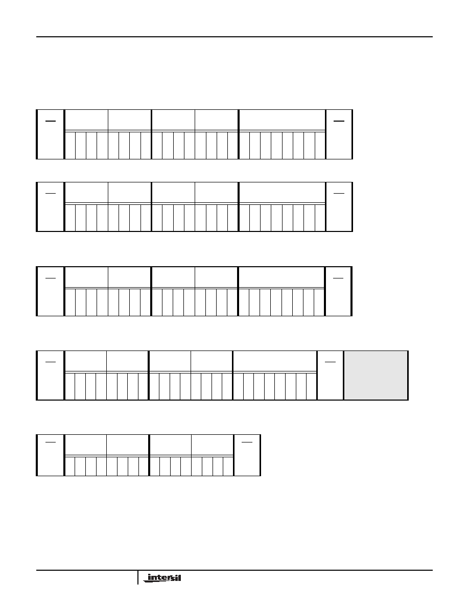
Figure 4. Two-Byte Instruction Sequence
0
1
0
1
1
1
0
A0
I3
I2
I1
I0
R1 R0
0
0
SCK
SI
CS
X9421
9
FN8196.1
September 23, 2005
Figure 5. Three-Byte Instruction Sequence (Write)
Figure 6. Three-Byte Instruction Sequence (Read)
Figure 7. Increment/Decrement Instruction Sequence
Figure 8. Increment/Decrement Timing Limits
0
1
0
1
0
A0
I3
I2
I1 I0
R1 R0 0
0
SCL
SI
0
0
D5 D4 D3 D2 D1 D0
CS
1
1
0
1
0
1
0
A0
I3
I2
I1 I0
R1 R0 0
0
SCL
SI
CS
1
1
S0
0
0
D5 D4 D3 D2 D1 D0
Don't Care
0
1
0
1
1
1
0
A0
I3
I2
I1
I0
0
0
0
SCK
SI
I
N
C
1
I
N
C
2
I
N
C
n
D
E
C
1
D
E
C
n
0
CS
SCK
SI
V
W
INC/DEC CMD Issued
t
WRID
Voltage Out
X9421

10
FN8196.1
September 23, 2005
Table 3. Instruction Set
Instruction
Instruction Set
Operation
I
3
I
2
I
1
I
0
R
1
R
0
Read Wiper Counter
Register
1
0
0
1
0
0
0
0
Read the contents of the Wiper Counter Register
Write Wiper Counter
Register
1
0
1
0
0
0
0
0
Write new value to the Wiper Counter Register
Read Data Register
1
0
1
1
1/0 1/0
0
0
Read the contents of the Data Register pointed to
by R
1
- R
0
Write Data Register
1
1
0
0
1/0 1/0
0
0
Write new value to the Data Register pointed to by
R
1
- R
0
XFR Data Register to
Wiper Counter
Register
1
1
0
1
1/0 1/0
0
0
Transfer the contents of the Data Register pointed
to by R
1
- R
0
to the Wiper Counter Register
XFR Wiper Counter
Register to Data
Register
1
1
1
0
1/0 1/0
0
0
Transfer the contents of the Wiper Counter
Register to the Data Register pointed to by R
1
- R
0
Increment/Decrement
Wiper Counter
Register
0
0
1
0
0
0
0
0
Enable Increment/decrement of the Wiper Counter
Register
Read Status (WIP bit)
0
1
0
1
0
0
0
1
Read the status of the internal write cycle, by
checking the WIP bit.
X9421
11
FN8196.1
September 23, 2005
Instruction Format
Notes: (1) "A0": stands for the device addresses sent by the master.
(2) WPx refers to wiper position data in the Wiper Counter Register
"I": stands for the increment operation, SI held HIGH during active SCK phase (high).
(3) "D": stands for the decrement operation, SI held LOW during active SCK phase (high).
Read Wiper Counter Register (WCR)
Write Wiper Counter Register (WCR)
Read Data Register (DR)
Read the contents of the Register pointed to by R1 - R0.
Write Data Register (DR)
Write a new value to the Register pointed to by R1 - R0.
Transfer Data Register (DR) to Wiper Counter Register (WCR)
Transfer the contents of the Register pointed to by R1 - R0 to the WCR.
CS
Falling
Edge
device type
identifier
device
addresses
instruction
opcode
wiper position
(sent by X9421 on SO)
CS
Rising
Edge
0 1 0 1 1 1 0 A
0 1 0 0 1 0 0 0 0 0 0
W
P
5
W
P
4
W
P
3
W
P
2
W
P
1
W
P
0
CS
Falling
Edge
device type
identifier
device
addresses
instruction
opcode
Data Byte
(sent by Host on SI)
CS
Rising
Edge
0 1 0 1 1 1 0 A
0 1 0 1 0 0 0 0 0 0 0
W
P
5
W
P
4
W
P
3
W
P
2
W
P
1
W
P
0
CS
Falling
Edge
device type
identifier
device
addresses
instruction
opcode
register
addresses
Data Byte
(sent by X9421 on SO)
CS
Rising
Edge
0 1 0 1 1 1 0 A
0 1 0 1 1
R
1
R
0 0 0 0 0
W
P
5
W
P
4
W
P
3
W
P
2
W
P
1
W
P
0
CS
Falling
Edge
device type
identifier
device
addresses
instruction
opcode
register
addresses
Data Byte
(sent by host on SI)
CS
Rising
Edge
HIGH-VOLTAGE
WRITE CYCLE
0 1 0 1 1 1 0 A
0 1 1 0 0
R
1
R
0 0 0 0 0
W
P
5
W
P
4
W
P
3
W
P
2
W
P
1
W
P
0
CS
Falling
Edge
device type
identifier
device
addresses
instruction
opcode
register
addresses
CS
Rising
Edge
0 1 0 1 1 1 0 A
0 1 1 0 1
R
1
R
0 0 0
X9421
12
FN8196.1
September 23, 2005
Transfer Wiper Counter Register (WCR) to Data Register (DR)
Increment/Decrement Wiper Counter Register (WCR)
Read Status
CS
Falling
Edge
device type
identifier
device
addresses
instruction
opcode
register
addresses
CS
Rising
Edge
HIGH-VOLTAGE
WRITE CYCLE
0 1 0 1 1 1 0 A
0 1 1 1 0
R
1
R
0 0 0
CS
Falling
Edge
device type
identifier
device
addresses
instruction
opcode
increment/decrement
(sent by master on SDA)
CS
Rising
Edge
0 1 0 1 1 1 0 A
0 0 0 1 0 0 0 0 0 I/D I/D .
.
.
. I/D I/D
CS
Falling
Edge
device type
identifier
device
addresses
instruction
opcode
Data Byte
(sent by X9421 on SO)
CS
Rising
Edge
0 1 0 1 1 1 0 A
0 0 1 0 1 0 0 0 1 0 0 0 0 0 0 0
W
I
P
X9421
13
FN8196.1
September 23, 2005
ABSOLUTE MAXIMUM RATINGS
Temperature under bias. . . . . . . . . . . . .-65
∞
C to +135
∞
C
Storage temperature . . . . . . . . . . . . . . .-65
∞
C to +150
∞
C
Voltage on SCK any address input
with respect to V
SS
. . . . . . . . . . . . . . . . . .-1V to +7V
V = | (V
H
- V
L
) | . . . . . . . . . . . . . . . . . . . . . . . . . . . . . 5V
Lead temperature (soldering, 10 seconds) . . . . . . 300
∞
C
I
W
(10 seconds) . . . . . . . . . . . . . . . . . . . . . . . . .±6mA
Any V
H
/R
H
, V
L
/R
L
, V
W
/R
W
. . . . . . . . . . . V
SS
to V
CC
COMMENT
Stresses above those listed under "Absolute Maximum
Ratings" may cause permanent damage to the device.
This is a stress rating only; functional operation of the
device (at these or any other conditions above those
listed in the operational sections of this specification)
is not implied. Exposure to absolute maximum rating
conditions for extended periods may affect device
reliability.
ANALOG CHARACTERISTICS (Over recommended operating conditions unless otherwise stated.)
Notes: (1) Absolute Linearity is utilized to determine actual wiper voltage versus expected voltage as determined by wiper position when used as
a potentiometer.
(2) Relative Linearity is utilized to determine the actual change in voltage between two successive tap positions when used as a
potentiometer. It is a measure of the error in step size.
(3) MI = RTOT/63 or (V
H
- V
L
)/63, single pot
(4) Typical = Individual array resolution.
Symbol
Parameter
Limits
Test Conditions
Min.
Typ.
Max.
Units
End to End Resistance Tolerance
±20
%
Power Rating
50
mW
25∞C, each pot
I
W
Wiper Current
±3
mA
R
W
Wiper Resistance
150
250
Wiper Current =
±
1mA,
V
CC
= 5V
400
1000
Wiper Current =
±
1mA,
V
CC
= 3V
V
TERM
Voltage on any V
H
/R
H
, V
L
/R
L
, V
W
/R
W
V
SS
V
CC
V
V
SS
= 0V
Noise
-120
dBV
Ref: 1kHz
Resolution
(4)
1.6
%
See Note 5
Absolute Linearity
(1)
±1
MI
(3)
V
w(n)(actual)
- V
w(n)(expected)
Relative Linearity
(2)
±0.2
MI
(3)
V
w(n + 1)
- [V
w(n) + MI
]
Temperature Coefficient of R
TOTAL
±
300
ppm/∞C
See Note 5
Ratiometric Temperature
Coefficient
±
20
ppm/∞C
See Note 5
C
H
/C
L
/C
W
Potentiometer Capacitances
10/10/25
pF
See Circuit #3
I
AL
Rh, RI, Rw leakage current
0.1
10
µA
Vin = Vss to Vcc. Device is in
stand-by mode.
RECOMMENDED OPERATING CONDITIONS
Temp
Min.
Max.
Commercial
0
∞
C
+70
∞
C
Industrial
-40
∞
C
+85
∞
C
Device
Supply Voltage (V
CC
) Limits
X9421
5V
±
10%
X9421-2.7
2.7V to 5.5V
X9421
14
FN8196.1
September 23, 2005
D.C. OPERATING CHARACTERISTICS (Over the recommended operating conditions unless otherwise specified.)
ENDURANCE AND DATA RETENTION
CAPACITANCE
POWER-UP TIMING
POWER-UP REQUIREMENTS (Power-up sequencing can affect correct recall of the wiper registers)
The preferred power-on sequence is as follows: First V
CC
and then the potentiometer pins, R
H
, R
L
, and R
W
. Voltage
should not be applied to the potentiometer pins before V
CC
is applied. The V
CC
ramp rate specification should be
met, and any glitches or slope changes in the V
CC
line should be held to <100mV if possible. Also, V
CC
should not
reverse polarity by more than 0.5V. Recall of wiper position will not be complete until V
CC
reaches its final value.
Notes: (5) This parameter is periodically sampled and not 100% tested.
A.C. TEST CONDITIONS
Symbol
Parameter
Limits
Test Conditions
Min.
Typ.
Max.
Units
I
CC1
V
CC
Supply Current
(Active)
400
µA
f
SCK
= 2MHz, SO = Open,
Other Inputs = V
SS
I
CC2
V
CC
Supply Current
(Non-volatile Write)
1
mA
f
SCK
= 2MHz, SO = Open,
Other Inputs = V
SS
I
SB
V
CC
Current (Standby)
1
µ
A
SCK = SI = V
SS
, Addr. = V
SS
I
LI
Input Leakage Current
10
µ
A
V
IN
= V
SS
to V
CC
I
LO
Output Leakage Current
10
µ
A
V
OUT
= V
SS
to V
CC
V
IH
Input HIGH Voltage
V
CC
x 0.7
V
CC
+ 0.5
V
V
IL
Input LOW Voltage
-0.5
V
CC
x 0.1
V
V
OL
Output LOW Voltage
0.4
V
I
OL
= 3mA
Parameter
Min.
Units
Minimum Endurance
100,000
Data Changes per Bit per Register
Data Retention
100
Years
Symbol
Test
Max.
Units
Test Conditions
C
OUT
(5)
Output Capacitance (SO)
8
pF
V
OUT
= 0V
C
IN
(5)
Input Capacitance (A0, SI, and SCK)
6
pF
V
IN
= 0V
Symbol
Parameter Max.
Max.
Units
t
R
V
CC
(5)
V
CC
Power-up Ramp
0.2
50
V/msec
Input pulse levels
V
CC
x 0.1 to V
CC
x
0.9
Input rise and fall times
10ns
Input and output timing level
V
CC
x 0.5
X9421
15
FN8196.1
September 23, 2005
EQUIVALENT A.C. LOAD CIRCUIT
Circuit #3 SPICE Macro Model
AC TIMING
5V
1533
100pF
SDA Output
2.7V
100pF
10pF
R
H
R
TOTAL
C
H
25pF
C
W
C
L
10pF
R
W
R
L
Symbol
Parameter
Min.
Max.
Units
f
SCK
SSI/SPI Clock Frequency
2.0
MHz
t
CYC
SSI/SPI Clock Cycle Time
500
ns
t
WH
SSI/SPI Clock High Time
200
ns
t
WL
SSI/SPI Clock Low Time
200
ns
t
LEAD
Lead Time
250
ns
t
LAG
Lag Time
250
ns
t
SU
SI, SCK, HOLD and CS Input Setup Time
50
ns
t
H
SI, SCK, HOLD and CS Input Hold Time
50
ns
t
RI
SI, SCK, HOLD and CS Input Rise Time
2
µs
t
FI
SI, SCK, HOLD and CS Input Fall Time
2
µs
t
DIS
SO Output Disable Time
0
500
ns
t
V
SO Output Valid Time
100
ns
t
HO
SO Output Hold Time
0
ns
t
RO
SO Output Rise Time
50
ns
t
FO
SO Output Fall Time
50
ns
t
HOLD
HOLD Time
400
ns
t
HSU
HOLD Setup Time
100
ns
t
HH
HOLD Hold Time
100
ns
t
HZ
HOLD Low to Output in High Z
100
ns
t
LZ
HOLD High to Output in Low Z
100
ns
T
I
Noise Suppression Time Constant at SI, SCK, HOLD and CS inputs
20
ns
t
CS
CS Deselect Time
2
µs
t
WPASU
WP, A0 and A1 Setup Time
0
ns
t
WPAH
WP, A0 and A1 Hold Time
0
ns
X9421
16
FN8196.1
September 23, 2005
HIGH-VOLTAGE WRITE CYCLE TIMING
XDCP TIMING
SYMBOL TABLE
Symbol
Parameter
Typ.
Max.
Units
t
WR
High-voltage Write Cycle Time (Store Instructions)
5
10
ms
Symbol
Parameter
Min.
Max. Units
t
WRPO
Wiper Response Time After The Third (Last) Power Supply Is Stable
10
µs
t
WRL
Wiper Response Time After Instruction Issued (All Load Instructions)
10
µs
t
WRID
Wiper Response Time From An Active SCL/SCK Edge (Increment/Decrement
Instruction)
450
ns
WAVEFORM
INPUTS
OUTPUTS
Must be
steady
Will be
steady
May change
from Low to
High
Will change
from Low to
High
May change
from High to
Low
Will change
from High to
Low
Don't Care:
Changes
Allowed
Changing:
State Not
Known
N/A
Center Line
is High
Impedance
X9421
17
FN8196.1
September 23, 2005
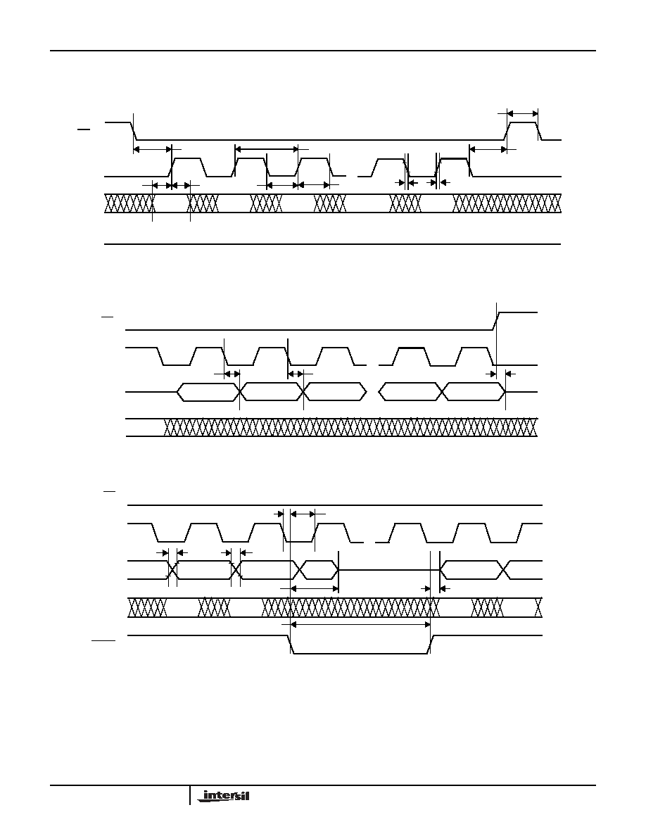
TIMING DIAGRAMS
Input Timing
Output Timing
Hold Timing
...
CS
SCK
SI
SO
MSB
LSB
High Impedance
t
LEAD
t
H
t
SU
t
FI
t
CS
t
LAG
t
CYC
t
WL
...
t
RI
t
WH
...
CS
SCK
SO
SI
ADDR
MSB
LSB
t
DIS
t
HO
t
V
...
...
CS
SCK
SO
SI
HOLD
t
HSU
t
HH
t
LZ
t
HZ
t
HOLD
t
RO
t
FO
X9421

18
FN8196.1
September 23, 2005
XDCP Timing (for All Load Instructions)
XDCP Timing (for Increment/Decrement Instruction)
Write Protect and Device Address Pins Timing
...
CS
SCK
SI
MSB
LSB
V
W
t
WRL
...
SO
High Impedance
...
CS
SCK
SO
SI
ADDR
t
WRID
High Impedance
V
W
...
Inc/Dec
Inc/Dec
...
CS
WP
A0
A1
t
WPASU
t
WPAH
(Any Instruction)
X9421
19
FN8196.1
September 23, 2005
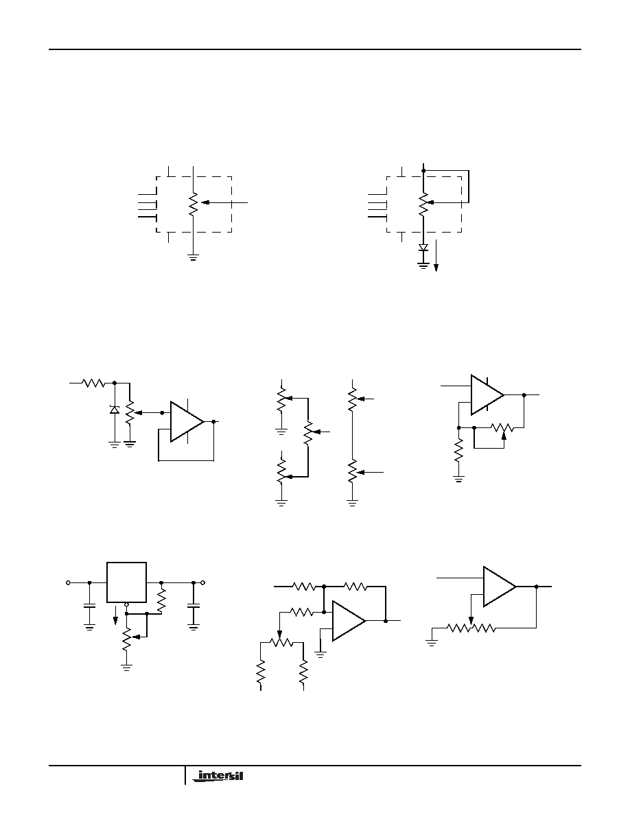
APPLICATIONS INFORMATION
Electronic potentiometers provide three powerful application advantages: (1) the variability and reliability of a solid-
state potentiometer, (2) the flexibility of computer-based digital controls, and (3) the retentivity of nonvolatile memory
used for the storage of multiple potentiometer settings or data.
Basic Configurations of Electronic Potentiometers
Basic Circuits
V
R
V
W
V
R
I
Three terminal Potentiometer;
Variable voltage divider
Two terminal Variable Resistor;
Variable current
V
H
V
L
Noninverting Amplifier
Voltage Regulator
Offset Voltage Adjustment
Comparator with Hysterisis
+
≠
V
S
V
O
R
2
R
1
V
O
= (1+R
2
/R
1
)V
S
R
1
R
2
I
adj
V
O
(REG) = 1.25V (1+R
2
/R
1
)+I
adj
R
2
V
O
(REG)
V
IN
317
+
≠
V
S
V
O
R
2
R
1
V
UL
= {R
1
/CR
1
+R
2
} V
O
(max)
V
LL
= {R
1
/CR
1
+R
2
} V
O
(min)
100k
10k
10k
10k
-12V
+12V
TL072
+
≠
V
S
V
O
R
2
R
1
}
}
+5V
-5V
LM308A
Cascading Techniques
Buffered Reference Voltage
≠
+
+5V
R
1
+V
-5V
V
W
V
W
V
OUT
= V
W
OP-07
V
W
V
W
+V
+V
+V
X
(a)
(b)
X9421
20
FN8196.1
September 23, 2005
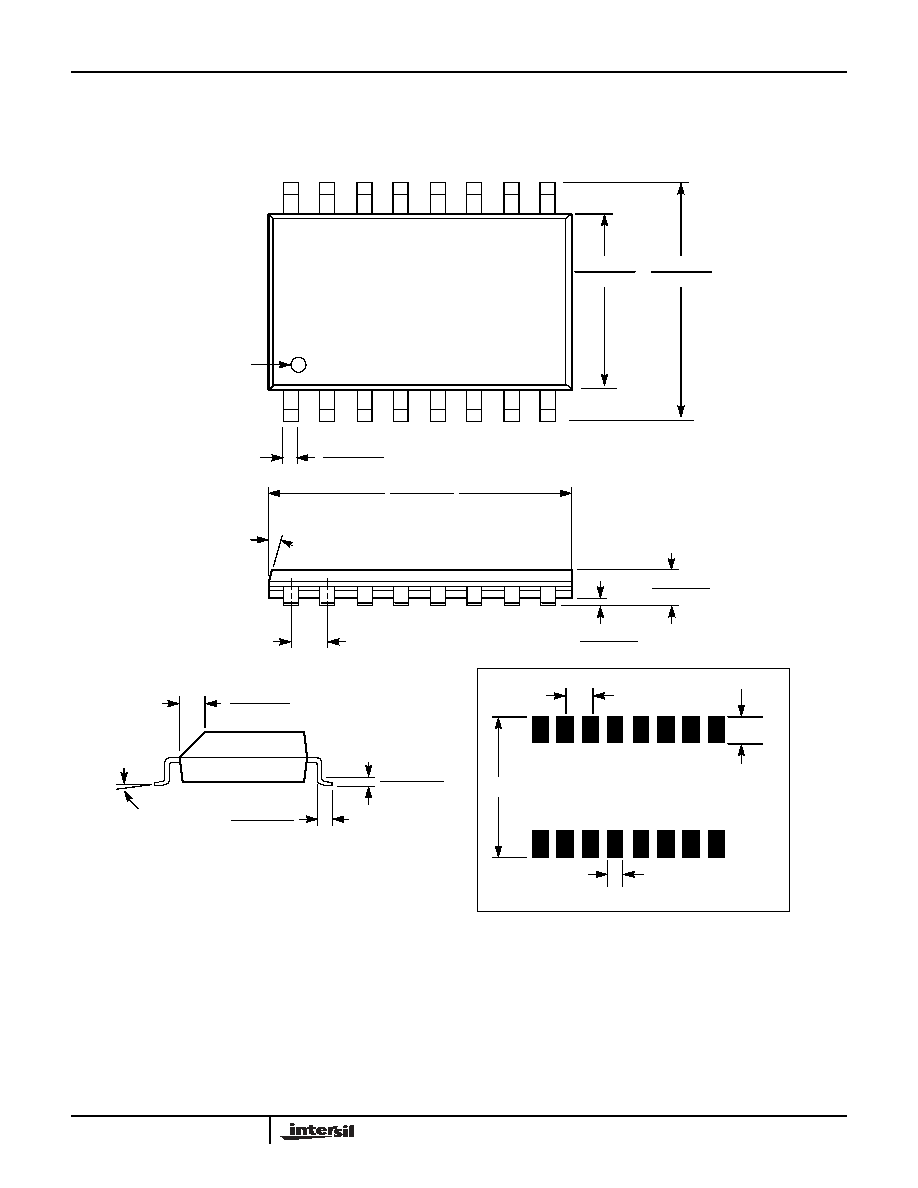
PACKAGING INFORMATION
16-Lead Plastic SOIC (300 Mil Body) Package Type S
NOTE: ALL DIMENSIONS IN INCHES (IN PARENTHESES IN MILLIMETERS)
0.014 (0.35)
0.020 (0.51)
PIN 1
PIN 1 INDEX
0.050 (1.27)
0.403 (10.2 )
0.413 ( 10.5)
(4X) 7∞
0.420"
0.050" Typical
0.030" Typical
16 Places
FOOTPRINT
0.010 (0.25)
0.020 (0.50)
0.0075 (0.19)
0.010 (0.25)
0
∞ - 8 ∞
X 45
∞
0.050"
Typical
0.290 (7.37)
0.299 (7.60)
0.393 (10.00)
0.420 (10.65)
0.003 (0.10)
0.012 (0.30)
0.092 (2.35)
0.105 (2.65)
0.015 (0.40)
0.050 (1.27)
X9421
21
All Intersil U.S. products are manufactured, assembled and tested utilizing ISO9000 quality systems.
Intersil Corporation's quality certifications can be viewed at www.intersil.com/design/quality
Intersil products are sold by description only. Intersil Corporation reserves the right to make changes in circuit design, software and/or specifications at any time without
notice. Accordingly, the reader is cautioned to verify that data sheets are current before placing orders. Information furnished by Intersil is believed to be accurate and
reliable. However, no responsibility is assumed by Intersil or its subsidiaries for its use; nor for any infringements of patents or other rights of third parties which may result
from its use. No license is granted by implication or otherwise under any patent or patent rights of Intersil or its subsidiaries.
For information regarding Intersil Corporation and its products, see www.intersil.com
FN8196.1
September 23, 2005
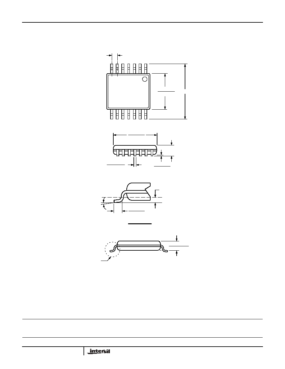
PACKAGING INFORMATION
NOTE: ALL DIMENSIONS IN INCHES (IN PARENTHESES IN MILLIMETERS)
14-Lead Plastic, TSSOP, Package Type V
See Detail "A"
.031 (.80)
.041 (1.05)
.169 (4.3)
.177 (4.5) .252 (6.4) BSC
.025 (.65) BSC
.193 (4.9)
.200 (5.1)
.002 (.05)
.006 (.15)
.047 (1.20)
.0075 (.19)
.0118 (.30)
0∞ - 8∞
.010 (.25)
.019 (.50)
.029 (.75)
Gage Plane
Seating Plane
Detail A (20X)
X9421