1
Æ
FN8197.0
CAUTION: These devices are sensitive to electrostatic discharge; follow proper IC Handling Procedures.
1-888-INTERSIL or 1-888-352-6832
|
Intersil (and design) is a registered trademark of Intersil Americas Inc.
XDCP is a trademark of Intersil Americas Inc. Copyright Intersil Americas Inc. 2005. All Rights Reserved
All other trademarks mentioned are the property of their respective owners.
X9428
Low Noise/Low Power/2-Wire Bus
Single Digitally Controlled Potentiometer
(XDCPTM)
FEATURES
∑ Solid state potentiometer
∑ 2-wire serial interface
∑ Register oriented format
--Direct Read/Write/Transfer Wiper Position
--Store as many as Four Positions per
Potentiometer
∑ Power supplies
--V
CC
= 2.7V to 5.5V
--V+ = 2.7V to 5.5V
--V≠ = -2.7V to -5.5V
∑ Low power CMOS
--Standby current < 1µA
--Ideal for Battery Operated Applications
∑ High reliability
--Endurance≠100,000 Data Changes per Bit per
Register
--Register Data Retention≠100 years
∑ 4-bytes of nonvolatile memory
∑ 10k
resistor array
∑ Resolution: 64 taps each potentiometer
∑ SOIC and TSSOP packages
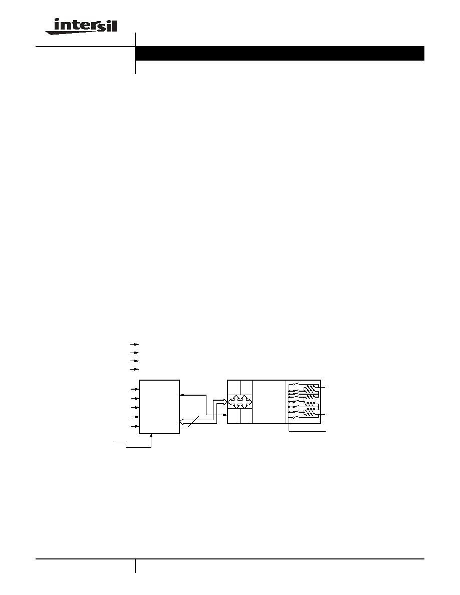
DESCRIPTION
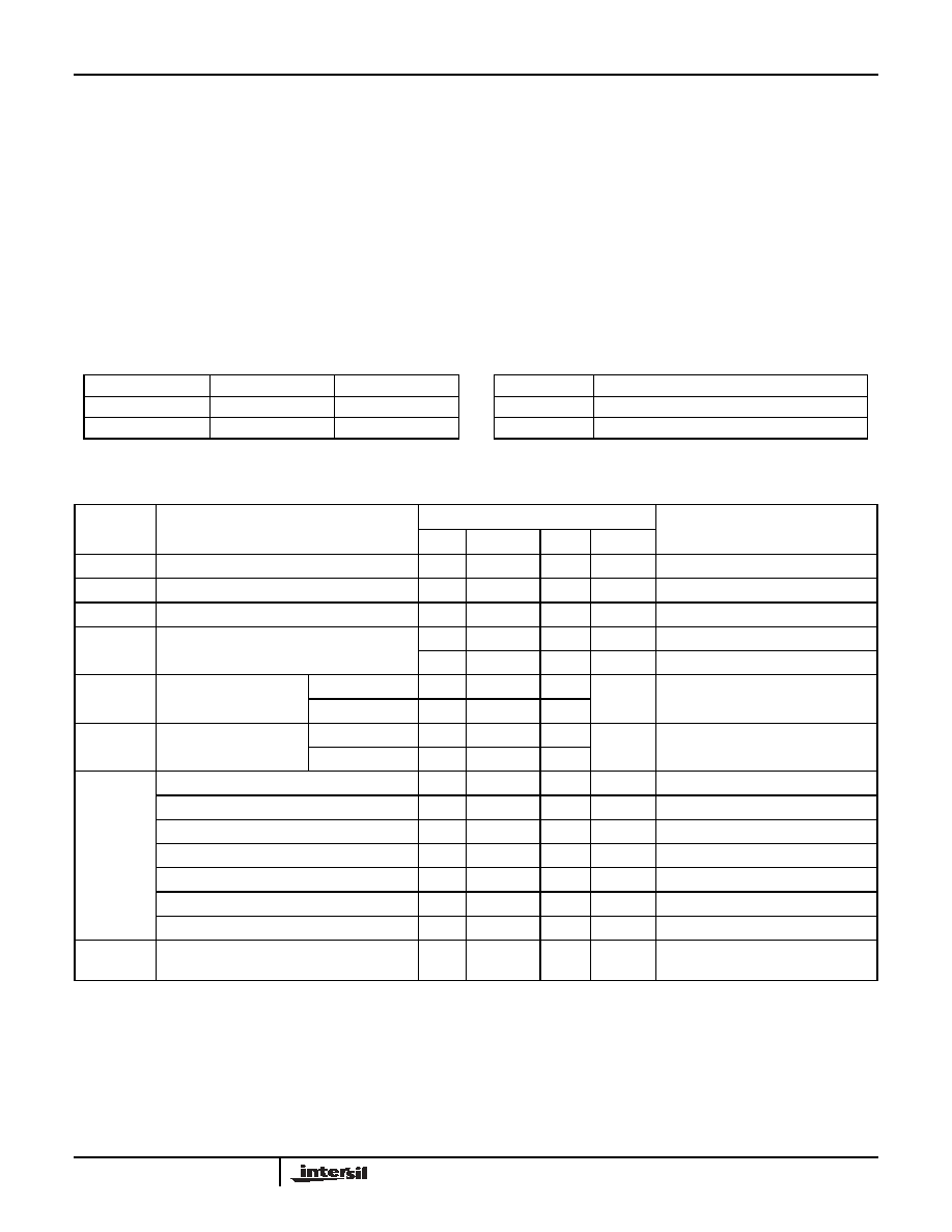
The X9428 integrates a digitally controlled
potentiometers (XDCP) on a monolithic CMOS
integrated microcircuit.
The digitally controlled potentiometer is implemented
using 63 resistive elements in a series array. Between
each element are tap points connected to the wiper
terminal through switches. The position of the wiper on
the array is controlled by the user through the 2-wire
bus interface. Each potentiometer has associated with
it a volatile Wiper Counter Register (WCR) and 4
nonvolatile Data Registers (DR0:DR3) that can be
directly written to and read by the user. The contents
of the WCR controls the position of the wiper on the
resistor array through the switches. Power-up recalls
the contents of DR0 to the WCR.
The XDCP can be used as a three-terminal
potentiometer or as a two-terminal variable resistor in
a wide variety of applications including control,
parameter adjustments, and signal processing.
BLOCK DIAGRAM
R0 R1
R2 R3
Wiper
Counter
Register
(WCR)
Interface
and
Control
Circuitry
SCL
SDA
A0
A2
A3
V
H
/R
H
V
L
/R
L
Data
8
V
W
/R
W
WP
V
CC
V
SS
V+
V≠
Data Sheet
March 8, 2005
2
FN8197.0
March 8, 2005
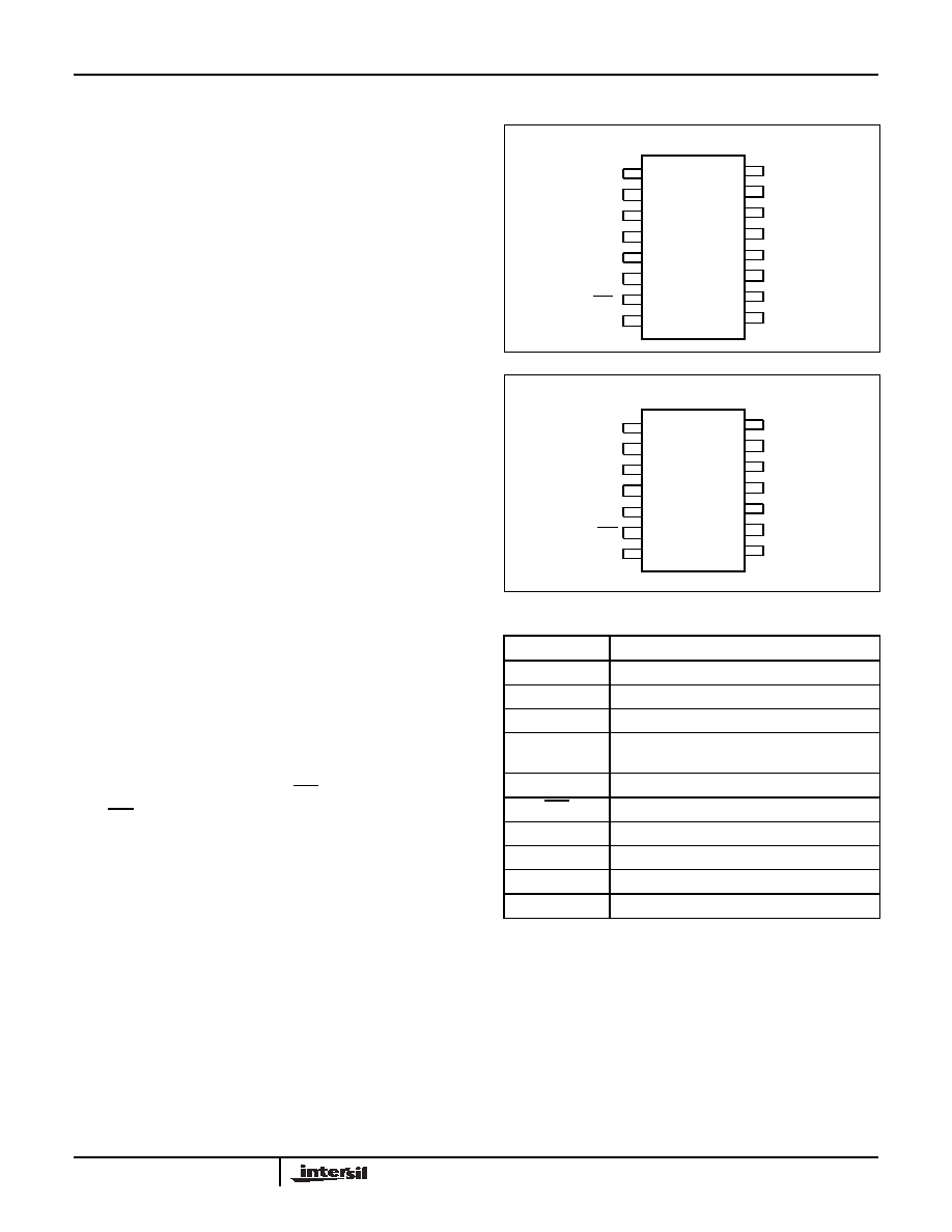
PIN DESCRIPTIONS
Host Interface Pins
Serial Clock (SCL)
The SCL input is used to clock data into and out of the
X9428.
Serial Data (SDA)
SDA is a bidirectional pin used to transfer data into
and out of the device. It is an open drain output and
may be wire-ORed with any number of open drain or
open collector outputs. An open drain output requires
the use of a pull-up resistor. For selecting typical
values, refer to the guidelines for calculating typical
values on the bus pull-up resistors graph.
Device Address (A
0
, A
2
, A
3
)
The Address inputs are used to set the least
significant 3 bits of the 8-bit slave address. A match in
the slave address serial data stream must be made
with the Address input in order to initiate
communication with the X9428. A maximum of 8
devices may occupy the 2-wire serial bus.
Potentiometer Pins
R
H
/V
H
, R
L
/V
L
The R
H
/V
H
and R
L
/V
L
inputs are equivalent to the
terminal connections on either end of a mechanical
potentiometer.
R
W
/V
W
The wiper outputs are equivalent to the wiper output of
a mechanical potentiometer.
Hardware Write Protect Input WP
The WP pin when low prevents nonvolatile writes to
the Data Registers.
Analog Supply V+, V-
The Analog Supply V+, V- are the supply voltages for
the XDCP analog section.
PIN CONFIGURATION
PIN NAMES
Symbol
Description
SCL
Serial clock
SDA
Serial data
A0, A2, A3
Device address
R
H
/V
H
, V
L
/R
H
Potentiometer Pins
(terminal equivalent)
R
W
/V
W
Potentiometer Pin (wiper equivalent)
WP
Hardware write protection
V+,V-
Analog and voltage follower
V
CC
System supply voltage
V
SS
System ground
NC
No connection
V
CC
A2
R
L
/V
L
SDA
WP
1
2
3
4
5
6
7
8
16
15
14
13
12
11
10
9
V+
NC
A0
NC
A3
SCL
NC
V-
DIP/SOIC
X9428
V
SS
R
H
/V
H
R
W
/V
W
1
2
3
4
5
6
7
14
13
12
11
10
9
8
TSSOP
X9428
A2
R
L
SDA
WP
V
SS
R
H
R
W
V
CC
V+
A0
NC
A3
SCL
V-
X9428

3
FN8197.0
March 8, 2005
PRINCIPLES OF OPERATION
The X9428 is a highly integrated microcircuit
incorporating a resistor array and its associated
registers and counters and the serial interface logic
providing direct communication between the host and
the XDCP potentiometers.
Serial Interface
The X9428 supports a bidirectional bus oriented
protocol. The protocol defines any device that sends
data onto the bus as a transmitter and the receiving
device as the receiver. The device controlling the
transfer is a master and the device being controlled is
the slave. The master will always initiate data transfers
and provide the clock for both transmit and receive
operations. Therefore, the X9428 will be considered a
slave device in all applications.
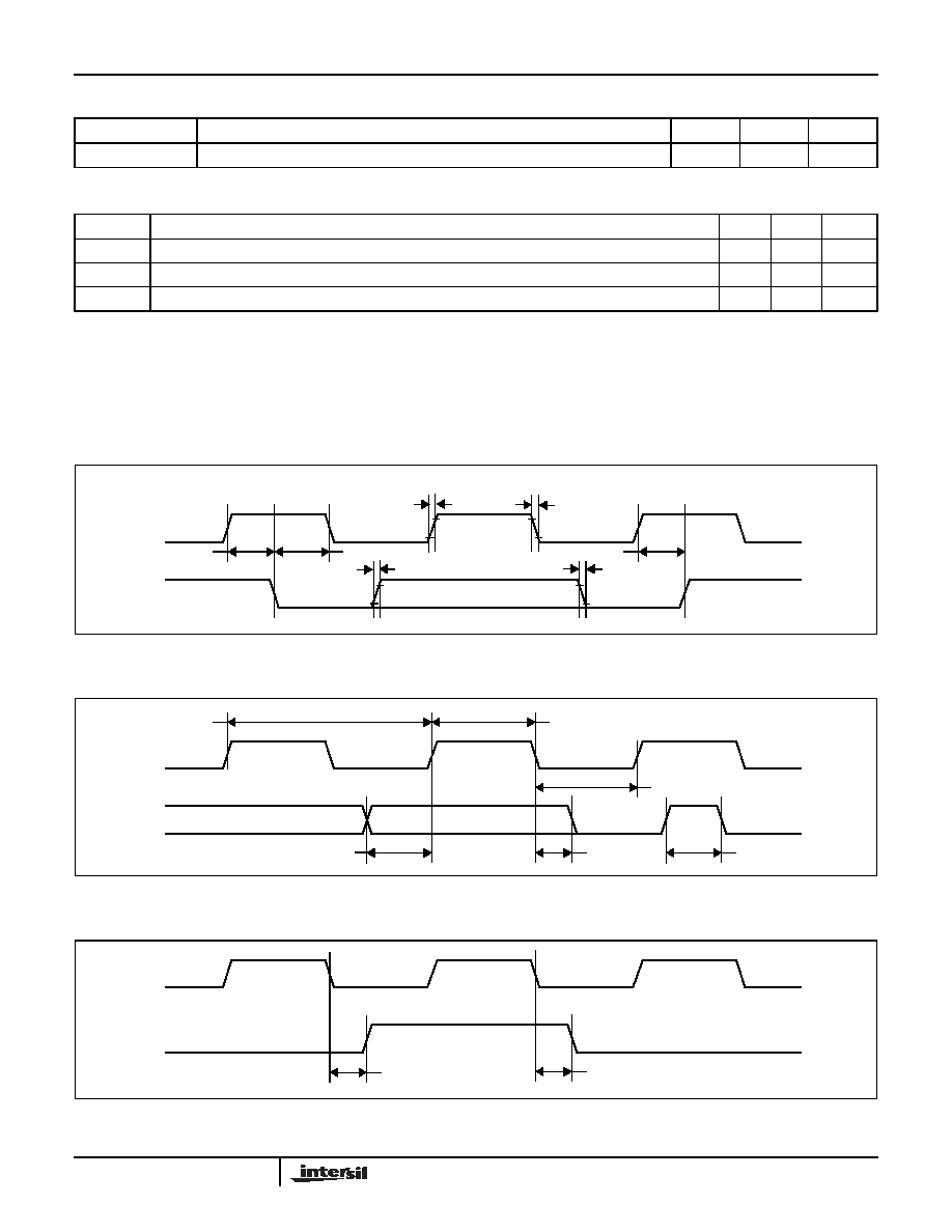
Clock and Data Conventions
Data states on the SDA line can change only during
SCL LOW periods (tLOW). SDA state changes during
SCL HIGH are reserved for indicating start and stop
conditions.
Start Condition
All commands to the X9428 are preceded by the start
condition, which is a HIGH to LOW transition of SDA
while SCL is HIGH (t
HIGH
). The X9428 continuously
monitors the SDA and SCL lines for the start condition
and will not respond to any command until this
condition is met.
Stop Condition
All communications must be terminated by a stop
condition, which is a LOW to HIGH transition of SDA
while SCL is HIGH.
Acknowledge
Acknowledge is a software convention used to provide
a positive handshake between the master and slave
devices on the bus to indicate the successful receipt of
data. The transmitting device, either the master or the
slave, will release the SDA bus after transmitting eight
bits. The master generates a ninth clock cycle and
during this period the receiver pulls the SDA line LOW
to acknowledge that it successfully received the eight
bits of data.
The X9428 will respond with an acknowledge after
recognition of a start condition and its slave address
and once again after successful receipt of the
command byte. If the command is followed by a data
byte the X9428 will respond with a final acknowledge.
Array Description
The X9428 is comprised of a resistor array. The array
contains 63 discrete resistive segments that are
connected in series. The physical ends of the array
are equivalent to the fixed terminals of a mechanical
potentiometer (V
H
/R
H
and V
L
/R
L
inputs).
At both ends of the array and between each resistor
segment is a CMOS switch connected to the wiper
(V
W
/R
W
) output. Within each individual array only one
switch may be turned on at a time. These switches are
controlled by the Wiper Counter Register (WCR). The
six bits of the WCR are decoded to select, and enable,
one of sixty-four switches.
The WCR may be written directly, or it can be changed
by transferring the contents of one of four associated
Data Registers into the WCR. These Data Registers and
the WCR can be read and written by the host system.
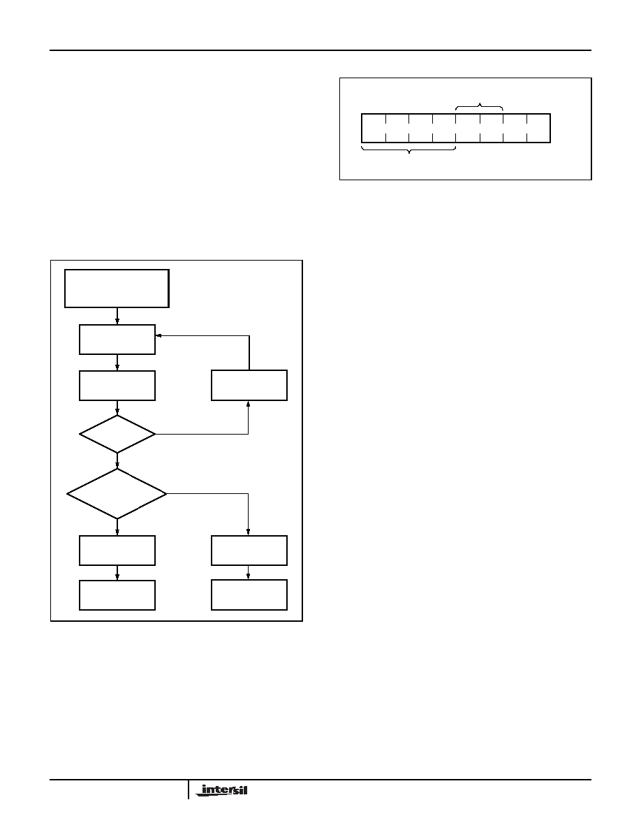
Device Addressing
Following a start condition the master must output the
address of the slave it is accessing. The most
significant four bits of the slave address are the device
type identifier (refer to Figure 1 below). For the X9428
this is fixed as 0101[B].
Figure 1. Slave Address
The next four bits of the slave address are the device
address. The physical device address is defined by
the state of the A
0
, A
2
, A
3
inputs. The X9428
compares the serial data stream with the address
input state; a successful compare of all four address
bits is required for the X9428 to respond with an
acknowledge. The A
0
, A
2
, A
3
inputs can be actively
driven by CMOS input signals or tied to V
CC
or V
SS
.
1
0
0
A3
A2
0
A0
Device Type
Identifier
Device Address
1
X9428
4
FN8197.0
March 8, 2005
Acknowledge Polling
The disabling of the inputs, during the internal
nonvolatile write operation, can be used to take
advantage of the typical 5ms EEPROM write cycle
time. Once the stop condition is issued to indicate the
end of the nonvolatile write command the X9428
initiates the internal write cycle. ACK polling can be
initiated immediately. This involves issuing the start
condition followed by the device slave address. If the
X9428 is still busy with the write operation no ACK will
be returned. If the X9428 has completed the write
operation an ACK will be returned, and the master can
then proceed with the next operation.
Flow 1. ACK Polling Sequence
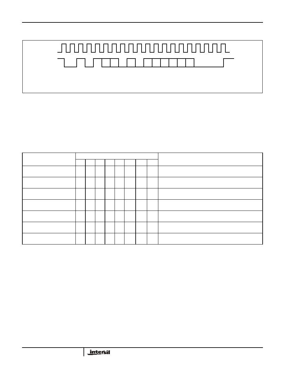
Instruction Structure
The next byte sent to the X9428 contains the instruction
and register pointer information. The four most
significant bits are the instruction. The next four bits
point to one of four associated registers. The format is
shown below in Figure 2.
Figure 2. Instruction Byte Format
The four high order bits define the instruction. The next
two bits (R1 and R0) select one of the four registers that
is to be acted upon when a register oriented instruction
is issued. Bits 0 and 1 are defined to be 0.
Four of the seven instructions end with the transmission
of the instruction byte. The basic sequence is illustrated
in Figure 3. These two-byte instructions exchange data
between the Wiper Counter Register and one of the
Data Registers. A transfer from a Data Register to a
Wiper Counter Register is essentially a write to a static
RAM. The response of the wiper to this action will be
delayed t
WRL
. A transfer from the Wiper Counter
Register (current wiper position), to a Data Register is a
write to nonvolatile memory and takes a minimum of
t
WR
to complete.
Four instructions require a three-byte sequence to
complete. These instructions transfer data between the
host and the X9428; either between the host and one of
the Data Registers or directly between the host and the
Wiper Counter Register. These instructions are: Read
Wiper Counter Register (read the current wiper position
of the selected pot), write Wiper Counter Register
(change current wiper position of the selected pot), read
Data Register (read the contents of the selected
nonvolatile register) and write Data Register (write a
new value to the selected Data Register). The
sequence of operations is shown in Figure 4.
Nonvolatile Write
Command Completed
Enter ACK Polling
Issue
START
Issue Slave
Address
ACK
Returned?
Further
Operation?
Issue
Instruction
Issue STOP
NO
YES
YES
Proceed
Issue STOP
NO
Proceed
I1
I2
I3
I0
R1
R0
0
0
Register
Select
Instructions
X9428
5
FN8197.0
March 8, 2005
Figure 3. Two-Byte Instruction Sequence
The Increment/Decrement command is different from
the other commands. Once the command is issued
and the X9428 has responded with an acknowledge,
the master can clock the selected wiper up and/or
down in one segment steps; thereby, providing a fine
tuning capability to the host. For each SCL clock pulse
(t
HIGH
) while SDA is HIGH, the selected wiper will
move one resistor segment towards the V
H
/R
H
terminal. Similarly, for each SCL clock pulse while
SDA is LOW, the selected wiper will move one resistor
segment towards the V
L
/R
L
terminal. A detailed
illustration of the sequence and timing for this
operation are shown in Figures 5 and 6 respectively.
Table 1. Instruction Set
Note:
(7) 1/0 = data is one or zero
S
T
A
R
T
0
1
0
1
A3 A2
0
A0
A
C
K
I3
I2
I1
I0
R1 R0 0
0
A
C
K
SCL
SDA
S
T
O
P
Instruction
Instruction Set
Operation
I
3
I
2
I
1
I
0
R
1
R
0
X
1
X
0
Read Wiper Counter
Register
1
0
0
1
0
0
0
0
Read the contents of the Wiper Counter Register
Write Wiper Counter
Register
1
0
1
0
0
0
0
0
Write new value to the Wiper Counter Register
Read Data Register
1
0
1
1
1/0 1/0
0
0
Read the contents of the Data Register pointed to by
R
1
- R
0
Write Data Register
1
1
0
0
1/0 1/0
0
0
Write new value to the Data Register pointed to by
R
1
- R
0
XFR Data Register to
Wiper Counter Register
1
1
0
1
1/0 1/0
0
0
Transfer the contents of the Data Register pointed to
by R
1
- R
0
to its Wiper Counter Register
XFR Wiper Counter
Register to Data Register
1
1
1
0
1/0 1/0
0
0
Transfer the contents of the Wiper Counter Register
to the Data Register pointed to by R
1
- R
0
Increment/Decrement
Wiper Counter Register
0
0
1
0
0
0
0
1/0 Enable Increment/decrement of the Wiper Counter
Register
X9428
6
FN8197.0
March 8, 2005
Figure 4. Three-Byte Instruction Sequence
Figure 5. Increment/Decrement Instruction Sequence
Figure 6. Increment/Decrement Timing Limits
S
T
A
R
T
0
1
0
1
A3 A2 0
A0 A
C
K
I3
I2
I1 I0
R1 R0 0
0
A
C
K
SCL
SDA
S
T
O
P
A
C
K
0
0
D5 D4 D3 D2 D1 D0
S
T
A
R
T
0
1
0
1
A3 A2 0
A0
A
C
K
I3
I2
I1
I0
R0 0
0
A
C
K
SCL
SDA
S
T
O
P
X
X
I
N
C
1
I
N
C
2
I
N
C
n
D
E
C
1
D
E
C
n
R1
SCL
SDA
V
W
/R
W
INC/DEC
CMD
Issued
Voltage Out
t
WRID
X9428
7
FN8197.0
March 8, 2005
Figure 7. Acknowledge Response from Receiver
Figure 8. Detailed Potentiometer Block Diagram
SCL from
Data Output
from Transmitter
1
8
9
START
Acknowledge
Master
Data Output
from Receiver
Serial Data Path
From Interface
Circuitry
Register 0
Register 1
Register 2
Register 3
Serial
Bus
Input
Parallel
Bus
Input
Wiper
Counter
Register
INC/DEC
Logic
UP/DN
CLK
Modified SCL
UP/DN
V
H
/R
H
V
L
/R
L
V
W
/R
W
If WCR = 00[H] then V
W
/R
W
= V
L
/R
L
If WCR = 3F[H] then V
W
/R
W
= V
H
/R
H
8
6
C
o
u
n
t
e
r
D
e
c
o
d
e
(WCR)
X9428

8
FN8197.0
March 8, 2005
DETAILED OPERATION
The potentiometer has a Wiper Counter Register and
four Data Registers. A detailed discussion of the
register organization and array operation follows.
Wiper Counter Register
The X9428 contains a Wiper Counter Register. The
Wiper Counter Register can be envisioned as a 6-bit
parallel and serial load counter with its outputs
decoded to select one of sixty-four switches along its
resistor array. The contents of the WCR can be altered
in four ways: it may be written directly by the host via
the write Wiper Counter Register instruction (serial
load); it may be written indirectly by transferring the
contents of one of four associated Data Registers via
the XFR Data Register instruction (parallel load); it can
be modified one step at a time by the
Increment/Decrement instruction. Finally, it is loaded
with the contents of its Data Register zero (DR0) upon
power-up.
The WCR is a volatile register; that is, its contents are
lost when the X9428 is powered-down. Although the
register is automatically loaded with the value in DR0
upon power-up, it should be noted this may be
different from the value present at power-down.
Data Registers
The potentiometer has four nonvolatile Data
Registers. These can be read or written directly by the
host and data can be transferred between any of the
four Data Registers and the Wiper Counter Register. It
should be noted all operations changing data in one of
these registers is a nonvolatile operation and will take
a maximum of 10ms.
If the application does not require storage of multiple
settings for the potentiometer, these registers can be
used as regular memory locations that could possibly
store system parameters or user preference data.
Register Descriptions
Data Registers, (6-Bit), Nonvolatile
Four 6-bit Data Registers for each XDCP. (eight 6-bit
registers in total).
≠ {D5~D0}: These bits are for general purpose not
volatile data storage or for storage of up to four
different wiper values. The contents of Data Register
0 are automatically moved to the Wiper Counter
Register on power-up.
Wiper Counter Register, (6-Bit), Volatile
One 6-bit wiper counter register for each XDCP. (Four
6-bit registers in total.)
≠ {D5~D0}: These bits specify the wiper position of the
respective XDCP. The Wiper Counter Register is
loaded on power-up by the value in Data Register 0.
The contents of the WCR can be loaded from any of
the other Data Register or directly. The contents of
the WCR can be saved in a DR.
D5
D4
D3
D2
D1
D0
NV
NV
NV
NV
NV
NV
(MSB)
(LSB)
WP5
WP4
WP3
WP2
WP1
WP0
V
V
V
V
V
V
(MSB)
(LSB)
X9428
9
FN8197.0
March 8, 2005
Instruction Format
Notes: (1) "MACK"/"SACK": stands for the acknowledge sent by the master/slave.
(2) "A3 ~ A0": stands for the device addresses sent by the master.
(3) "X": indicates that it is a "0" for testing purpose but physically it is a "don't care" condition.
(4) "I": stands for the increment operation, SDA held high during active SCL phase (high).
(5) "D": stands for the decrement operation, SDA held low during active SCL phase (high).
Read Wiper Counter Register (WCR)
Write Wiper Counter Register (WCR)
Read Data Register (DR)
Write Data Register (DR)
XFR Data Register (DR) to Wiper Counter Register (WCR)
S
T
A
R
T
device type
identifier
device
addresses
S
A
C
K
instruction
opcode
S
A
C
K
wiper position
(sent by slave on SDA)
M
A
C
K
S
T
O
P
0 1 0 1 A
3
A
2 0
A
0
1 0 0 1 0 0 0 0
0 0
W
P
5
W
P
4
W
P
3
W
P
2
W
P
1
W
P
0
S
T
A
R
T
device type
identifier
device
addresses
S
A
C
K
instruction
opcode
S
A
C
K
wiper position
(sent by master on SDA)
S
A
C
K
S
T
O
P
0 1 0 1 A
3
A
2 0
A
0
1 0 1 0 0 0 0 0
0 0
W
P
5
W
P
4
W
P
3
W
P
2
W
P
1
W
P
0
S
T
A
R
T
device type
identifier
device
addresses
S
A
C
K
instruction
opcode
register
addresses
S
A
C
K
wiper position/data
(sent by slave on SDA)
M
A
C
K
S
T
O
P
0 1 0 1 A
3
A
2 0
A
0
1 0 1 1 R
1
R
0 0 0
0 0
W
P
5
W
P
4
W
P
3
W
P
2
W
P
1
W
P
0
S
T
A
R
T
device type
identifier
device
addresses
S
A
C
K
instruction
opcode
register
addresses
S
A
C
K
wiper position/data
(sent by master on SDA)
S
A
C
K
S
T
O
P
HIGH-VOLTAGE
WRITE CYCLE
0 1 0 1 A
3
A
2 0
A
0
1 1 0 0 R
1
R
0 0 0
0 0
W
P
5
W
P
4
W
P
3
W
P
2
W
P
1
W
P
0
S
T
A
R
T
device type
identifier
device
addresses
S
A
C
K
instruction
opcode
register
addresses
S
A
C
K
S
T
O
P
0 1 0 1 A
3
A
2 0
A
0
1 1 0 1 R
1
R
0 0 0
X9428
10
FN8197.0
March 8, 2005
XFR Wiper Counter Register (WCR) to Data Register (DR)
Increment/Decrement Wiper Counter Register (WCR)
SYMBOL TABLE
Guidelines for Calculating Typical Values of Bus
Pull-Up Resistors
S
T
A
R
T
device type
identifier
device
addresses
S
A
C
K
instruction
opcode
register
addresses
S
A
C
K
S
T
O
P
HIGH-VOLTAGE
WRITE CYCLE
0 1 0 1 A
3
A
2 0
A
0
1 1 1 0 R
1
R
0 0 0
S
T
A
R
T
device type
identifier
device
addresses
S
A
C
K
instruction
opcode
S
A
C
K
increment/decrement
(sent by master on SDA)
S
T
O
P
0 1 0 1 A
3
A
2 0
A
0
0 0 1 0 0 0 0 0
I/
D
I/
D .
.
.
. I/
D
I/
D
WAVEFORM
INPUTS
OUTPUTS
Must be
steady
Will be
steady
May change
from Low to
High
Will change
from Low to
High
May change
from High to
Low
Will change
from High to
Low
Don't Care:
Changes
Allowed
Changing:
State Not
Known
N/A
Center Line
is High
Impedance
120
100
80
40
60
20
20 40 60 80 100 120
0
0
Resist
ance
(K)
Bus Capacitance (pF)
Min.
Resistance
Max.
Resistance
R
MAX
=
C
BUS
t
R
R
MIN
=
I
OL MIN
V
CC MAX
=1.8k
X9428
11
FN8197.0
March 8, 2005
ABSOLUTE MAXIMUM RATINGS
Temperature under bias .................... -65
∞
C to +135
∞
C
Storage temperature ......................... -65
∞
C to +150
∞
C
Voltage on SDA, SCL or any address
input with respect to V
SS
......................... -1V to +7V
Voltage on V+ (referenced to V
SS
)........................ 10V
Voltage on V- (referenced to V
SS
)........................-10V
(V+) - (V-) .............................................................. 12V
Any V
H
/R
H
..............................................................V+
Any V
L
/R
L
.................................................................V-
Lead temperature (soldering, 10 seconds)........ 300
∞
C
I
W
(10 seconds)................................................±12mA
COMMENT
Stresses above those listed under "Absolute Maximum
Ratings" may cause permanent damage to the device.
This is a stress rating only; functional operation of the
device (at these or any other conditions above those
listed in the operational sections of this specification)
is not implied. Exposure to absolute maximum rating
conditions for extended periods may affect device
reliability.
ANALOG CHARACTERISTICS (Over recommended operating conditions unless otherwise stated.)
Symbol
Parameter
Limits
Test Conditions
Min.
Typ.
Max.
Unit
End to end resistance tolerance
±20
%
Power rating
50
mW
25∞C, each pot
I
W
Wiper current
±6
mA
R
W
Wiper resistance
150
250
Wiper current =
±
1mA, V
CC
= 3V
40
100
Wiper current =
±
1mA, V
CC
= 5V
V+
Voltage on V+ pin
X9428
+4.5
+5.5
V
X9428-2.7
+2.7
+5.5
V-
Voltage on V- pin
X9428
-5.5
-4.5
V
X9428-2.7
-5.5
-2.7
V
TERM
Voltage on any V
H
/R
H
or V
L
/R
L
pin
V-
V+
V
Noise
-140
dBV
Ref: 1kHz
Resolution
(4)
1.6
%
Absolute linearity
(1)
±1
MI
(3)
V
w(n)(actual)
- V
w(n)(expected)
Relative linearity
(2)
±0.2
MI
(3)
V
w(n + 1 )
- [V
w(n) + MI
]
Temperature Coefficient of R
TOTAL
±
300
ppm/
∞
C
Ratiometric Temperature Coefficient
±20
ppm/∞C
C
H
/C
L
/C
W
Potentiometer Capacitances
10/10/25
pF
See Circuit #3,
Spice Macromodel
RECOMMENDED OPERATING CONDITIONS
Temp
Min.
Max.
Commercial
0
∞
C
+70
∞
C
Industrial
-40
∞
C
+85
∞
C
Device
Supply Voltage (V
CC
) Limits
X9428
5V
±
10%
X9428-2.7
2.7V to 5.5V
X9428
12
FN8197.0
March 8, 2005
D.C. OPERATING CHARACTERISTICS (Over the recommended operating conditions unless otherwise specified.)
Notes: (1) Absolute linearity is utilized to determine actual wiper voltage versus expected voltage as determined by wiper position when used as a
potentiometer.
(2) Relative linearity is utilized to determine the actual change in voltage between two successive tap positions when used as a potentiom-
eter. It is a measure of the error in step size.
(3) MI = RTOT/63 or (R
H
- R
L
)/63, single pot
(4) Max. = all four arrays cascaded together, Typical = individual array resolutions.
ENDURANCE AND DATA RETENTION
CAPACITANCE
POWER-UP TIMING
POWER-UP AND POWER-DOWN
There are no restrictions on the power-up or power-down sequencing of the bias supplies V
CC
, V+, and V- provided
that all three supplies reach their final values within 1msec of each other. However, at all times, the voltages on the
potentiometer pins must be less than V+ and more than V-. The recall of the wiper position from nonvolatile memory
is not in effect until all supplies reach their final value.
Notes: (5) This parameter is periodically sampled and not 100% tested
(6) t
PUR
and t
PUW
are the delays required from the time the third (last) power supply (V
CC
, V+ or V-) is stable until the specific
instruction can be issued. These parameters are periodically sampled and not 100% tested.
(7) Sample tested only.
Symbol
Parameter
Limits
Test Conditions
Min.
Typ.
Max.
Unit
I
CC1
V
CC
supply current
(nonvolatile write)
1
mA
f
SCL
= 400kHz, SDA = Open,
Other Inputs = V
SS
I
CC2
V
CC
supply current
(move wiper, write, read)
100
µA
f
SCL
= 400kHz, SDA = Open,
Other Inputs = V
SS
I
SB
V
CC
current (standby)
1
µA
SCL = SDA = V
CC
, Addr. = V
SS
I
LI
Input leakage current
10
µA
V
IN
= V
SS
to V
CC
I
LO
Output leakage current
10
µA
V
OUT
= V
SS
to V
CC
V
IH
Input HIGH voltage
V
CC
x 0.7
V
CC
x 0.5
V
V
IL
Input LOW voltage
-0.5
V
CC
x 0.1
V
V
OL
Output LOW voltage
0.4
V
I
OL
= 3mA
Parameter
Min.
Unit
Minimum endurance
100,000
Data changes per bit per register
Data retention
100
Years
Symbol
Test
Max.
Unit
Test Conditions
C
I/O
(5)
Input/output capacitance (SDA)
8
pF
V
I/O
= 0V
C
IN
(5)
Input capacitance (A0, A1, A2, A3, and SCL)
6
pF
V
IN
= 0V
Symbol
Parameter Min.
Typ.
Max.
Unit
t
PUR
(6)
Power-up to initiation of read operation
1
ms
t
PUW
(6)
Power-up to initiation of write operation
5
ms
t
R
V
CC
(7)
V
CC
Power-up ramp rate
0.2
50
V/msec
X9428
13
FN8197.0
March 8, 2005
A.C. TEST CONDITIONS
EQUIVALENT A.C. LOAD CIRCUIT
Circuit #3 SPICE Macro Model
AC TIMING (over recommended operating conditions)
Input pulse levels
V
CC
x 0.1 to V
CC
x 0.9
Input rise and fall times
10ns
Input and output timing level
V
CC
x 0.5
5V
1533
100pF
SDA Output
2.7V
100pF
10pF
R
H
R
TOTAL
C
H
25pF
C
W
C
L
10pF
R
W
R
L
Symbol
Parameter
Min.
Max.
Unit
f
SCL
Clock frequency
100
400
kHz
t
CYC
Clock cycle time
2500
ns
t
HIGH
Clock high time
600
ns
t
LOW
Clock low time
1300
ns
t
SU:STA
Start setup time
600
ns
t
HD:STA
Start hold time
600
ns
t
SU:STO
Stop setup time
600
ns
t
SU:DAT
SDA data input setup time
100
ns
t
HD:DAT
SDA data input hold time
30
ns
t
R
SCL and SDA rise time
300
ns
t
F
SCL and SDA fall time
300
ns
t
AA
SCL low to SDA data output valid time
900
ns
t
DH
SDA data output hold time
50
ns
T
I
Noise suppression time constant at SCL and SDA inputs
50
ns
t
BUF
Bus free time (prior to any transmission)
1300
ns
t
SU:WPA
WP, A0, A1, A2 and A3 setup time
0
ns
t
HD:WPA
WP, A0, A1, A2 and A3 hold time
0
ns
X9428
14
FN8197.0
March 8, 2005
HIGH-VOLTAGE WRITE CYCLE TIMING
XDCP TIMING
Note:
(8) A device must internally provide a hold time of at least 300ns for the SDA signal in order to bridge the undefined region of the falling
edge of SCL.
TIMING DIAGRAMS
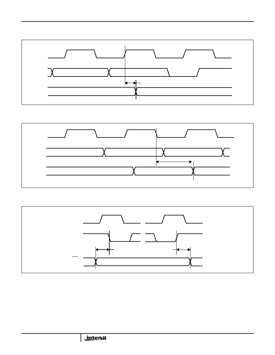
START and STOP Timing
Input Timing
Output Timing
Symbol
Parameter
Typ.
Max.
Unit
t
WR
High-voltage write cycle time (store instructions)
5
10
ms
Symbol
Parameter
Min.
Max.
Unit
t
WRPO
Wiper response time after the third (last) power supply is stable
10
µs
t
WRL
Wiper response time after instruction issued (all load instructions)
10
µs
t
WRID
Wiper response time from an active SCL/SCK edge (increment/decrement instruction)
10
µs
t
SU:STA
t
HD:STA
t
SU:STO
SCL
SDA
t
R
(START)
(STOP)
t
F
t
R
t
F
SCL
SDA
t
HIGH
t
LOW
t
CYC
t
HD:DAT
t
SU:DAT
t
BUF
SCL
SDA
t
DH
t
AA
X9428
15
FN8197.0
March 8, 2005
XDCP Timing (for All Load Instructions)
XDCP Timing (for Increment/Decrement Instruction)
Write Protect and Device Address Pins Timing
SCL
SDA
V
W
/R
W
(STOP)
LSB
t
WRL
SCL
SDA
V
W
/R
W
t
WRID
Wiper Register Address
Inc/Dec
Inc/Dec
SDA
SCL
...
...
...
WP
A0, A2, A3
t
SU:WPA
t
HD:WPA
(START)
(STOP)
(Any Instruction)
X9428
16
FN8197.0
March 8, 2005
APPLICATIONS INFORMATION
Basic Configurations of Electronic Potentiometers
Application Circuits
V
R
V
W
/R
W
+V
R
I
Three terminal Potentiometer;
Variable voltage divider
Two terminal Variable Resistor;
Variable current
Noninverting Amplifier
Voltage Regulator
Offset Voltage Adjustment
Comparator with Hysteresis
+
≠
V
S
V
O
R
2
R
1
V
O
= (1+R
2
/R
1
)V
S
R
1
R
2
I
adj
V
O
(REG) = 1.25V (1+R
2
/R
1
)+I
adj
R
2
V
O
(REG)
V
IN
317
+
≠
V
S
V
O
R
2
R
1
V
UL
= {R
1
/(R
1
+R
2
)} V
O
(max)
V
LL
= {R
1
/(R
1
+R
2
)} V
O
(min)
100k
10k
10k
10k
-12V
+12V
TL072
+
≠
V
S
V
O
R
2
R
1
}
}
X9428
17
FN8197.0
March 8, 2005
Application Circuits (continued)
Inverting Amplifier
Equivalent L-R Circuit
+
≠
V
S
V
O
R
2
R
1
Z
IN
= R
2
+ s R
2
(R
1
+ R
3
) C
1
= R
2
+ s Leq
(R
1
+ R
3
) >> R
2
+
≠
V
S
Function Generator
}
}
V
O
= G V
S
G = - R
2
/R
1
R
2
C
1
R
1
R
3
Z
IN
+
≠
R
2
+
≠
R
1
}
}
R
A
R
B
frequency
R
1
, R
2
, C
amplitude
R
A
, R
B
C
Attenuator
Filter
+
≠
V
S
V
O
R
3
R
1
V
O
= G V
S
-1/2
G
+1/2
G
O
= 1 + R
2
/R
1
fc = 1/(2
RC)
R
2
R
4
All R
S
= 10k
+
≠
V
S
R
2
R
1
R
C
V
O
X9428
18
FN8197.0
March 8, 2005
PACKAGING INFORMATION
NOTE: ALL DIMENSIONS IN INCHES (IN PARENTHESES IN MILLIMETERS)
14-Lead Plastic, TSSOP, Package Type V
See Detail "A"
.031 (.80)
.041 (1.05)
.169 (4.3)
.177 (4.5) .252 (6.4) BSC
.025 (.65) BSC
.193 (4.9)
.200 (5.1)
.002 (.05)
.006 (.15)
.047 (1.20)
.0075 (.19)
.0118 (.30)
0∞ - 8∞
.010 (.25)
.019 (.50)
.029 (.75)
Gage Plane
Seating Plane
Detail A (20X)
X9428
19
FN8197.0
March 8, 2005
PACKAGING INFORMATION
16-Lead Plastic SOIC (300 Mil Body) Package Type S
NOTE: ALL DIMENSIONS IN INCHES (IN PARENTHESES IN MILLIMETERS)
0.014 (0.35)
0.020 (0.51)
PIN 1
PIN 1 INDEX
0.050 (1.27)
0.403 (10.2 )
0.413 ( 10.5)
(4X) 7∞
0.420"
0.050" Typical
0.030" Typical
16 Places
FOOTPRINT
0.010 (0.25)
0.020 (0.50)
0.0075 (0.19)
0.010 (0.25)
0
∞ - 8 ∞
X 45
∞
0.050"
Typical
0.290 (7.37)
0.299 (7.60)
0.393 (10.00)
0.420 (10.65)
0.003 (0.10)
0.012 (0.30)
0.092 (2.35)
0.105 (2.65)
0.015 (0.40)
0.050 (1.27)
X9428
20
All Intersil U.S. products are manufactured, assembled and tested utilizing ISO9000 quality systems.
Intersil Corporation's quality certifications can be viewed at www.intersil.com/design/quality
Intersil products are sold by description only. Intersil Corporation reserves the right to make changes in circuit design, software and/or specifications at any time without
notice. Accordingly, the reader is cautioned to verify that data sheets are current before placing orders. Information furnished by Intersil is believed to be accurate and
reliable. However, no responsibility is assumed by Intersil or its subsidiaries for its use; nor for any infringements of patents or other rights of third parties which may result
from its use. No license is granted by implication or otherwise under any patent or patent rights of Intersil or its subsidiaries.
For information regarding Intersil Corporation and its products, see www.intersil.com
FN8197.0
March 8, 2005
Ordering Information
Device
V
CC
Limits
Blank = 5V ±10%
-2.7 = 2.7 to 5.5V
Temperature Range
Blank = Commercial = 0
∞
C to +70
∞
C
I = Industrial = -40
∞
C to +85
∞
C
Package
P = 16-Lead Plastic DIP*
S = 16-Lead SOIC
V = 14-Lead TSSOP
Potentiometer Organization
Y =
2k
W =
10k
X9428
P
T
V
Y
*Note: P package only available as X9428WP16I-2.7 for prototyping. Other resistor values not available in package.
X9428