 | –≠–Ľ–Ķ–ļ—ā—Ä–ĺ–Ĺ–Ĺ—č–Ļ –ļ–ĺ–ľ–Ņ–ĺ–Ĺ–Ķ–Ĺ—ā: X9430WV24 | –°–ļ–į—á–į—ā—Ć:  PDF PDF  ZIP ZIP |

1
ģ
FN8198.0
CAUTION: These devices are sensitive to electrostatic discharge; follow proper IC Handling Procedures.
1-888-INTERSIL or 1-888-352-6832
|
Intersil (and design) is a registered trademark of Intersil Americas Inc.
XDCP is a trademark of Intersil Americas Inc. Copyright Intersil Americas Inc. 2005. All Rights Reserved
All other trademarks mentioned are the property of their respective owners.
PRELIMINARY
X9430
Programmable Analog
Dual Digitally Controlled Potentiometer
(XDCPTM) with Operational Amplifier
FEATURES
∑ Two CMOS voltage operational amplifiers
∑ Two digitally controlled potentiometers
∑ Can be combined or used separately
∑ Amplifiers
--Low voltage operation
--V+/V- = Ī2.7V to Ī5.5V
--Rail-to-rail CMOS performance
--1MHz gain bandwidth product
∑ Digitally controlled potentiometer
--Dual 64 tap potentiometers
--R
total
= 10k
--SPI serial interface
--V
CC
= 2.7V to 5.5V
DESCRIPTION
The X9430 is a monolithic CMOS IC that incorporates
two operational amplifiers and two nonvolatile digitally
controlled potentiometers. The amplifiers are CMOS
differential input voltage operational amplifiers with
near rail-to-rail outputs. All pins for the two amplifiers
are brought out of the package to allow combining
them with the potentiometers or using them as com-
plete stand-alone amplifiers.
The digitally controlled potentiometers consist of a
series string of 63 polycrystalline resistors that behave
as standard integrated circuit resistors. The SPI serial
port, common to both pots, allows the user to program
the connection of the wiper output to any of the resis-
tor nodes in the series string. The wiper position is
saved in the on board E2 memory to allow for nonvola-
tile restoration of the wiper position.
A wide variety of applications can be implemented
using the potentiometers and the amplifiers. A typical
application is to implement the amplifier as a wiper
buffer in circuits that use the potentiometer as a voltage
reference. The potentiometer can also be combined
with the amplifier yielding a digitally programmable gain
amplifier or programmable current source.
BLOCK DIAGRAM
V
OUT1
Control and
CS
SCK
SO
SI
A1
A0
+
≠
Memory
V
CC
V
NI0
V+
V-
R
W0
V
SS
V
OUT0
+
≠
V
NI1
V
INV1
V
INV0
R
H0
R
L0
R
W1
R
L1
R
H1
WCR1
WCR0
WP
HOLD
Data Sheet
March 11, 2005
NOT RE
COMME
NDED FO
R NEW D
ESIGNS
NO REC
OMMEN
DED RE
PLACEM
ENT
contact
our Tec
hnical S
upport C
enter at
1-888-IN
TERSIL
or www.
intersil.c
om/tsc

2
FN8198.0
March 11, 2005
PIN DESCRIPTIONS
Host Interface Pins
Serial Output (SO)
SO is a push/pull serial data output pin. During a read
cycle, data is shifted out on this pin. Data is clocked
out by the falling edge of the serial clock.
Serial Input (SI)
SI is the serial data input pin. All opcodes, byte
addresses and data to be written to the device are
input on this pin. Data is latched by the rising edge of
the serial clock.
Serial Clock (SCK)
The SCK input is used to clock data into and out of the
X9430.
Chip Select (CS)
When CS is HIGH, the X9430 is deselected and the
SO pin is at high impedance, and (unless an internal
write cycle is underway) the device will be in the
standby state. CS LOW enables the X9430, placing it
in the active power mode. It should be noted that after
a power-up, a HIGH to LOW transition on CS is
required prior to the start of any operation.
Hardware Write Protect Input WP
The WP pin when low prevents nonvolatile writes to
the wiper counter register.
Hold (HOLD)
HOLD is used in conjunction with the CS pin to select
the device. Once the part is selected and a serial
sequence is underway, HOLD may be used to pause
the serial communication with the controller without
resetting the serial sequence. To pause, HOLD must
be brought LOW while SCK is LOW. To resume com-
munication, HOLD is brought HIGH, again while SCK
is LOW. If the pause feature is not used, HOLD should
be held HIGH at all times.
Device Address (A
0
- A
1
)
The address inputs are used to set the least significant
2 bits of the 8-bit slave address. A match in the slave
address serial data stream must be made with the
address input in order to initiate communication with
the X9430. A maximum of 4 devices may occupy the
SPI serial bus.
Potentiometer Pins
1
R
H
(R
H0
- R
H1
), R
L
(R
L0
- R
L1
)
The R
H
and R
L
inputs are equivalent to the terminal con-
nections on either end of a mechanical potentiometer.
R
W
(R
W0
- R
W1
)
The wiper output is equivalent to the wiper output of a
mechanical potentiometer.
Amplifier and Device Pins
Amplifier Input Voltage V
NI
(0,1) and V
INV
(0,1)
V
NI
and V
INV
are inputs to the noninverting (+) and
inverting (-) inputs of the operational amplifiers.
Amplifier Output Voltage V
OUT
(0,1)
V
OUT
is the voltage output pin of the operational
amplifier.
Analog Supplies V+, V-
The Analog Supplies V+, V- are the supply voltages
for the XDCP analog section and the operational
amplifiers.
System Supply V
CC
and Ground V
SS
The system supply V
CC
and its reference V
SS
is used
to bias the interface and control circuits.
1.
Alternate designations for R
H
, R
L
, R
W
are V
H
, V
L
, V
W
X9430
3
FN8198.0
March 11, 2005
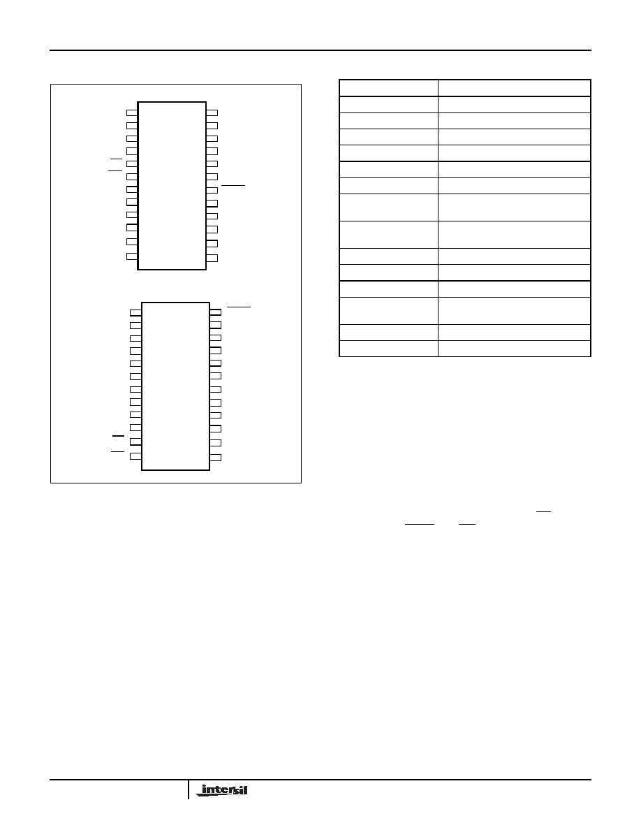
PIN CONFIGURATION
PIN NAMES
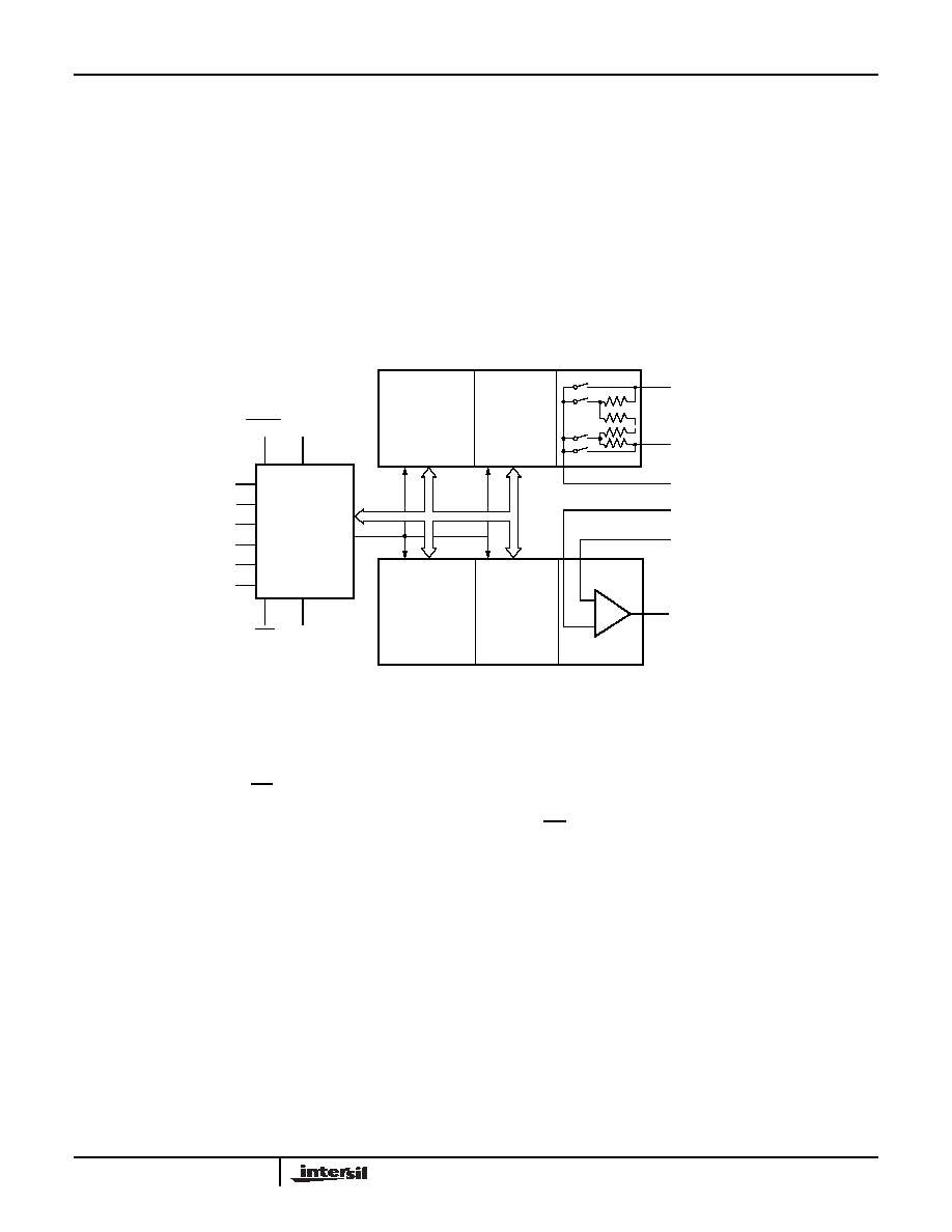
PRINCIPLES OF OPERATION
The X9430 is an integrated microcircuit incorporating two
digitally controlled potentiometers, two operational
amplifiers and their associated registers and counters;
and the serial interface logic providing direct communica-
tion between the host and the digitally controlled
potentiometers.
Serial Interface
The X9430 supports the SPI interface hardware con-
ventions. The device is accessed via the SI input with
data clocked in on the rising edge of SCK. CS must be
LOW and the HOLD and WP pins must be HIGH dur-
ing the entire operation.
V
CC
R
L0
R
H0
WP
A1
1
2
3
4
5
6
7
8
9
10
24
23
22
21
20
19
18
17
16
15
V+
V
OUT0
V
NI0
V
INV0
A0
S0
HOLD
SCK
V
INV1
V
NI1
SOIC
X9430
V
SS
R
W0
14
13
11
12
CS
R
L1
R
H1
R
W1
V
OUT1
V-
SI
V-
V
INV0
V
NI0
HOLD
SO
SCK
1
2
3
4
5
6
7
8
9
10
24
23
22
21
20
19
18
17
16
CS
V
CC
R
W0
TSSOP
X9430
V+
V
OUT0
11
12
A
0
V
OUT1
V
NI1
V
INV1
R
L0
R
H0
V
SS
R
W1
R
H1
R
L1
A
1
SI
WP
15
14
13
Symbol
Description
SCK
Serial Clock
SI
Serial Input
SO
Serial Output
A0 - A1
Device Address
CS
Chip Select
HOLD
Hold
R
H0
- R
H1
, R
L0
- R
L1
Potentiometers (terminal
equivalent)
R
W0
- R
W1
Potentiometers (wiper
equivalent)
V
NI(0,1)
, V
INV(0,1)
Amplifier Input Voltages
V
OUT0,
V
OUT1
Amplifier Outputs
WP
Hardware Write Protection
V+,V-
Analog and Voltage Amplifier
Supplies
V
CC
System/Digital Supply Voltage
V
SS
System Ground
X9430
4
FN8198.0
March 11, 2005
Potentiometer/Array Description
The X9430 is comprised of two resistor arrays and two
operational amplifiers. Each array contains 63 discrete
resistive segments that are connected in series. The
physical ends of each array are equivalent to the fixed
terminals of a mechanical potentiometer (R
H
and R
L
).
At both ends of each array and between each resistor
segment is a CMOS switch connected to the wiper
(R
W
) output. Within each individual array only one
switch may be turned on at a time. These switches are
controlled by a volatile wiper counter register (WCR).
The six bits of the WCR are decoded to select, and
enable, one of sixty-four switches.
The WCR may be written directly, or it can be changed
by transferring the contents of one of four associated
data registers into the WCR. These data registers and
the WCR can be read and written by the host system.
Operational Amplifier
The voltage operational amplifiers are CMOS rail-to-
rail output general purpose amplifiers. They are
designed to operate from dual (Ī) power supplies. The
amplifiers may be configured like any standard ampli-
fier. All pins are externally available to allow connec-
tion with the potentiometers or as stand alone
amplifiers.
Write in Process
The contents of the data registers are saved to nonvol-
atile memory when the CS pin goes from LOW to
HIGH after a complete write sequence is received by
the device. The progress of this internal write opera-
tion can be monitored by a write in process bit (WIP).
The WIP bit is read with a read status command.
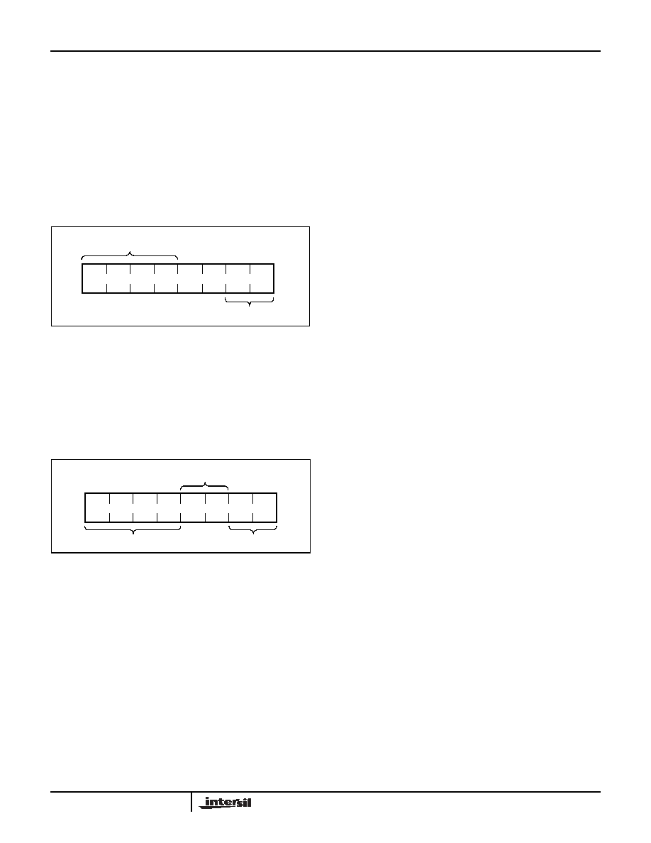
INSTRUCTIONS AND PROGRAMMING
Identification (ID) Byte
The first byte sent to the X9430 from the host, follow-
ing a CS going HIGH to LOW, is called the identifica-
tion byte. The most significant four bits of the slave
address are a device type identifier, for the X9430 this
is fixed as 0101[B] (refer to Figure 1).
Detailed Block Diagram
V
OUT (0,1)
(DR0 - DR3)
0,1
Control and
CS
SCK
SO
SI
A1
A0
V
H (0,1)
V
L (0,1)
WP
V
W (0,1)
V
N (0,1)
+
≠
WCR
0,1
(DR0 - DR3)
0,1
V
INV (0,1)
V
SS
V
CC
HOLD
Memory
WCR0
WCR1
(One of 2 Circuits)
X9430
5
FN8198.0
March 11, 2005
The two least significant bits in the ID byte select one
of four devices on the bus. The physical device
address is defined by the state of the A
0
- A
1
input
pins. The X9430 compares the serial data stream with
the address input state; a successful compare of both
address bits is required for the X9430 to successfully
continue the command sequence. The A
0
- A
1
inputs
can be actively driven by CMOS input signals or tied to
V
CC
or V
SS
.
The remaining two bits in the slave byte must be set to 0.
Figure 1. Identification Byte Format
Instruction Byte
The next byte sent to the X9430 contains the instruc-
tion and register pointer information. The four most
significant bits are the instruction. The next four bits
point to one of the WCRs of the two pots, and when
applicable, they point to one of four associated data
registers. The format is shown below in Figure 2.
Figure 2. Instruction Byte Format
The four high order bits of the instruction byte specify
the operation. The next two bits (R
1
and R
0
) select one
of the four registers that is to be acted upon when a
register oriented instruction is issued. The last bit (P
0
)
selects which one of the two potentiometers is to be
affected by the instruction.
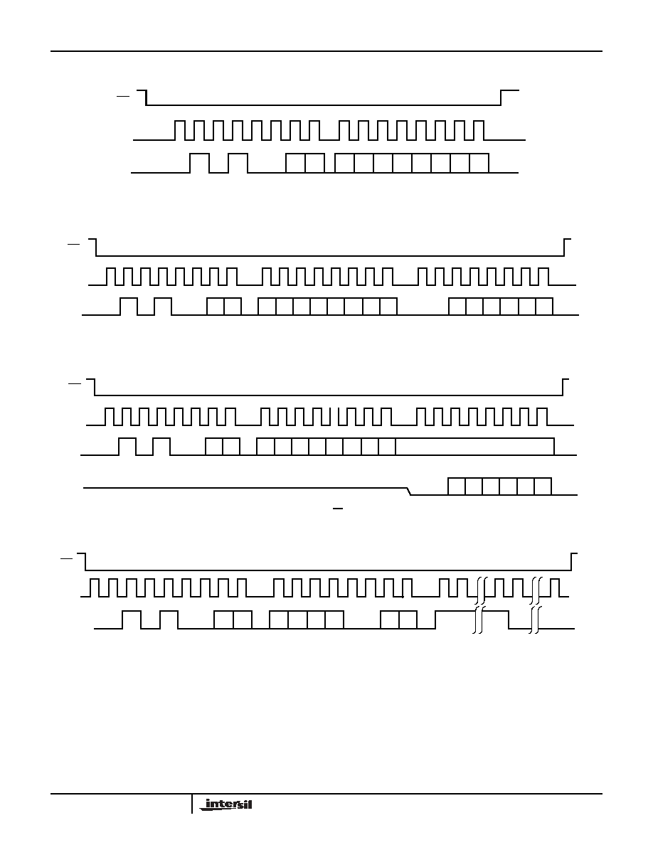
Four of the ten instructions are two bytes in length and
end with the transmission of the instruction byte.
The basic sequence of the two byte instructions is
illustrated in Figure 3. These two-byte instructions
exchange data between a wiper counter register and
one of the four data registers associated with each. A
transfer from a data register to a wiper counter register
is essentially a write to a static RAM. The response of
the wiper to this action will be delayed t
WRL
. A transfer
from the wiper counter register (current wiper position)
to a data register is a write to nonvolatile memory and
takes a minimum of t
WR
to complete. The transfer can
occur between one of the two potentiometers and one
of its associated registers; or it may occur globally,
wherein the transfer occurs between both of the poten-
tiometers and one of their associated registers.
Five instructions require a three-byte sequence to
complete. These instructions transfer data between
the host and the X9430; either between the host and
one of the data registers or directly between the host
and the Wiper Counter and Registers. These instruc-
tions are: 1) Read Wiper Counter Register, read the
current wiper position of the selected pot 2) Write
Wiper Counter Register, i.e. change current wiper
position of the selected pot; 3) Read Data Register,
read the contents of the selected nonvolatile register; 4)
Write Data Register, write a new value to the selected
data register; 5)Read Status, returns the contents of the
WIP bit which indicates if an internal write cycle is in
progress.
The sequence of these operations is shown in Figure
4 and Figure 5.
The final command is Increment/Decrement. It is differ-
ent from the other commands, because it's length is
indeterminate. Once the command is issued, the master
can clock the selected wiper up and/or down in one resis-
tor segment steps; thereby, providing a fine tuning capa-
bility to the host. For each SCK clock pulse (t
HIGH
) while
SI is HIGH, the selected wiper will move one resistor
segment towards the V
H
terminal. Similarly, for each
SCK clock pulse while SI is LOW, the selected wiper will
move one resistor segment towards the V
L
terminal. A
detailed illustration of the sequence and timing for this
operation are shown in Figure 6 and Figure 7.
1
0
0
0
0
A1
A0
Device Type
Identifier
Device Address
1
I1
I2
I3
I0
R1
R0
0
P0
WCR Select
Register
Select
Instructions
X9430
6
FN8198.0
March 11, 2005
Figure 3. Two Byte Command Sequence
Figure 4. Three-Byte Command Sequence (Write)
Figure 5. Three-Byte Command Sequence(Read)
Figure 6. Increment/Decrement Command Sequence
0
1
0
1
0
0
A1 A0
I3
I2
I1
I0
R1 R0 0
P0
SCK
SI
CS
0
1
0
1
A1 A0
I3
I2
I1 I0
R1 R0 0
P0
SCK
SI
0
0
D5 D4 D3 D2 D1 D0
CS
0
0
0
1
0
1
A1 A0
I3
I2
I1 I0
R1 R0 0
P0
SCK
SI
CS
0
0
S0
0
0
D5 D4 D3 D2 D1 D0
Don't Care
0
1
0
1
0
0
A1 A0
I3
I2
I1
I0
0
0
P0
SCK
SI
I
N
C
1
I
N
C
2
I
N
C
n
D
E
C
1
D
E
C
n
0
CS
X9430

7
FN8198.0
March 11, 2005
Figure 7. Increment/Decrement Timing
REGISTER OPERATION
Both digitally controlled potentiometers share the serial
interface and share a common architecture. Each poten-
tiometer is associated with a wiper counter register
(WCR), and four data registers. Figure 8 illustrates the
control, registers, and system features of the device.
Figure 8. System Block Diagram
Wiper Counter (WCR) and Analog Control
Registers (ACR)
The X9430 contains two wiper counter registers, one
for each XDCP. The wiper counter register is equiva-
lent to a serial-in, parallel-out counter with its outputs
decoded to select one of sixty-four switches along its
resistor array. The contents of the wiper counter register
can be altered in four ways: it may be written directly
by the host via the write WCR instruction (serial load);
it may be written indirectly by transferring the contents
of one of four associated data registers (DR) via the
XFR data register instruction (parallel load); it can be
modified one step at a time by the increment/decre-
ment instruction (WCR only). Finally, it may be loaded
with the contents of its associated data register zero
(R0) upon power-up.
The wiper counter register is a volatile register; that is, its
contents are lost when the X9430 is powered-down.
Although the registers are automatically loaded with the
value in R0 upon power-up, it should be noted this may
be different from the value present at power-down.
Data Registers (DR)
Each potentiometer has four nonvolatile data registers
(DR). These can be read or written directly by the host
and data can be transferred between any of the four data
registers and the WCR. It should be noted all operations
changing data in one of these registers is a nonvolatile
operation and will take a maximum of 10ms.
If the application does not require storage of multiple set-
tings for the potentiometer, these registers can be used
as regular memory locations that could store system
parameters or user preference data.
SCK
SI
V
W
INC/DEC CMD Issued
t
WRID
V
OUT
V
OUT (0,1)
(DR0-DR3)
0,1
Control and
CS
SCK
SO
SI
A1
A0
V
H (0,1)
V
L (0,1)
WP
V
W (0,1)
V
N (0,1)
+
≠
WCR
0,1
V
INV (0,1)
V
SS
V
CC
HOLD
Memory
WCR0
WCR1
Detailed Block Diagram
X9430
8
FN8198.0
March 11, 2005
REGISTER DESCRIPTIONS AND MEMORY MAP
Memory Map
Wiper Counter Register (WCR)
WP0 - WP5 identify wiper position.
Data Registers (DR, R0 - R3)
Instruction Format
Notes: (1) "A1 ~ A0": stands for the device addresses sent by the master.
(2) WPx refers to wiper position data in the Wiper Counter Register
(3) "I": stands for the increment operation, SI held HIGH during active SCK phase (high).
(4) "D": stands for the decrement operation, SI held LOW during active SCK phase (high).
Read Wiper Counter Register (WCR)
Read the contents of the Wiper Counter Register pointed to by P
1
- P
0
Write Wiper Counter Register (WCR)
Write new value to the Wiper Counter Register pointed to by P
1
- P
0
Read Data Register (DR)
Read the contents of the Register pointed to by P
1
- P
0
and R
1
- R
0
Write Data Register (DR)
Write new value to the Register pointed to by P
1
- P
0
and R
1
- R
0
WCRO
WCR1
DR0
DR0
DR1
DR1
DR2
DR2
DR3
DR3
0
0
WP5 WP4 WP3 WP2 WP1
WP0
(volatile)
(LSB)
Wiper Position or User Data
(Nonvolatile)
CS
Falling
Edge
device type
identifier
device
addresses
instruction
opcode
WCR
addresses
wiper position
(sent by X9430 on SO)
CS
Rising
Edge
0 1 0 1 0 0 A
1
A
0 1 0 0 1 0 0 0
P
0 0 0
W
P
5
W
P
4
W
P
3
W
P
2
W
P
1
W
P
0
CS
Falling
Edge
device type
identifier
device
addresses
instruction
opcode
WCR
addresses
Data Byte
(sent by Host on SI)
CS
Rising
Edge
0 1 0 1 0 0 A
1
A
0 1 0 1 0 0 0 0
P
0 0 0
W
P
5
W
P
4
W
P
3
W
P
2
W
P
1
W
P
0
CS
Falling
Edge
device type
identifier
device
addresses
instruction
opcode
DR/WCR
addresses
Data Byte
(sent by X9430 on SO)
CS
Rising
Edge
0 1 0 1 0 0 A
1
A
0 1 0 1 1
R
1
R
0 0
P
0 0 0
W
P
5
W
P
4
W
P
3
W
P
2
W
P
1
W
P
0
CS
Falling
Edge
device type
identifier
device
addresses
instruction
opcode
DR/WCR
addresses
Data Byte
(sent by host on SI)
CS
Rising
Edge
HIGH-VOLTAGE
WRITE CYCLE
0 1 0 1 0 0 A
1
A
0 1 1 0 0
R
1
R
0
0
P
0 0 0
W
P
5
W
P
4
W
P
3
W
P
2
W
P
1
W
P
0
X9430
9
FN8198.0
March 11, 2005
Transfer Data Register (DR) to Wiper Counter Register (WCR)
Transfer the contents of the Register pointed to by R
1
- R
0
to the WCR
Transfer Wiper Counter Register (WCR) to Data Register (DR)
Transfer the contents of the WCR to the Register pointed to by R
1
- R
0
Increment/Decrement Wiper Counter Register (WCR)
Enable Increment/decrement of the WCR pointed to by P
1
- P
0
Global Transfer Data Register (DR) to Wiper Counter Register (WCR)
Transfer the contents of all four Data Registers pointed to by R
1
- R
0
to their respective WCR
Global Transfer Wiper Counter Register (WCR) to Data Register (DR)
Transfer the contents of all WCRs to their respective data Registers pointed to by R
1
- R
0
Read Status
Returns the contents of the WIP bit which indicates if an internal write cycle is in progress
CS
Falling
Edge
device type
identifier
device
addresses
instruction
opcode
DR/WCR
addresses
CS
Rising
Edge
0 1 0 1 0 0 A
1
A
0 1 1 0 1
R
1
R
0
0 P
0
CS
Falling
Edge
device type
identifier
device
addresses
instruction
opcode
DR/WCR
addresses
CS
Rising
Edge
HIGH-VOLTAGE
WRITE CYCLE
0 1 0 1 0 0 A
1
A
0 1 1 1 0
R
1
R
0 0
P
0
CS
Falling
Edge
device type
identifier
device
addresses
instruction
opcode
WCR
addresses
increment/decrement
(sent by master on SDA)
CS
Rising
Edge
0 1 0 1 0 0 A
1
A
0 0 0 1 0 X X 0
P
0
I/
D
I/
D .
.
.
. I/
D
I/
D
CS
Falling
Edge
device type
identifier
device
addresses
instruction
opcode
DR
addresses
CS
Rising
Edge
0 1 0 1 0 0 A
1
A
0 0 0 0 1
R
1
R
0 0 0
CS
Falling
Edge
device type
identifier
device
addresses
instruction
opcode
DR
addresses
CS
Rising
Edge
HIGH-VOLTAGE
WRITE CYCLE
0 1 0 1 0 0 A
1
A
0 1 0 0 0
R
1
R
0 0 0
CS
Falling
Edge
device type
identifier
device
addresses
instruction
opcode
wiper
addresses
Data Byte
(sent by X9430 on SO)
CS
Rising
Edge
0 1 0 1 0 0 A
1
A
0 0 1 0 1 0 0 0 1 0 0 0 0 0 0 0
W
I
P
X9430
P
0
: 0-WCR0, 1-WCR1
10
FN8198.0
March 11, 2005
ABSOLUTE MAXIMUM RATINGS
Temperature under bias .................... -65
į
C to +135
į
C
Storage temperature ......................... -65
į
C to +150
į
C
Voltage on SCK, SCL or any
address input with respect to V
SS
........... -1V to +7V
Voltage on V+ (referenced to V
SS
) ........................+7V
Voltage on V- (referenced to V
SS
) ..........................-7V
(V+) - (V-) .............................................................. 10V
Any V
H
.....................................................................V+
Any V
L
......................................................................V-
Lead temperature (soldering, 10 seconds)........ 300
į
C
COMMENT
Stresses above those listed under "Absolute Maximum
Ratings" may cause permanent damage to the device.
This is a stress rating only; functional operation of the
device (at these or any other conditions above those
listed in the operational sections of this specification) is
not implied. Exposure to absolute maximum rating con-
ditions for extended periods may affect device reliability.
POTENTIOMETER CHARACTERISTICS (Over recommended operating conditions unless otherwise stated.)
Notes: (1) Absolute linearity is utilized to determine actual wiper voltage versus expected voltage as determined by wiper position when used as a
potentiometer.
(2) Relative linearity is utilized to determine the actual change in voltage between two successive tap positions when used as a
potentiometer. It is a measure of the error in step size.
(3) MI = RTOT/63 or (R
H
- R
L
)/63, single pot (=LSB)
(4) Individual array resolutions
Symbol
Parameter
Limits
Test Conditions
Min. Typ. Max.
Unit
R
TOTAL
End to end resistance
-20
+20
%
Power rating
50
mW
25
į
C, each pot
I
W
Wiper current
-3
+3
mA
R
W
Wiper resistance
40
100
V+ = 5V, V- = -5V, I
W
= 3mA
100
250
V+ = 2.7V, V- = -2.7V, I
W
= 1mA
Vv+
Voltage on V+ pin
X9430
+4.5
+5.5
V
X9430-2.7
+2.7
+5.5
Vv-
Voltage on V- pin
X9430
-5.5
-4.5
V
X9430-2.7
-5.5
-2.7
V
TERM
Voltage on any R
H
or R
L
pin
V-
V+
V
Noise
-100
dBv
Ref: 1V
Resolution
(4)
1.6
%
Absolute linearity
(1)
-1
+1
MI
(3)
V
w(n)(actual)
- V
w(n)(expected)
Relative linearity
(2)
-0.2
+0.2
MI
(3)
V
w(n + 1)
- [V
w(n) + MI
]
Temperature coefficient of R
TOTAL
Ī
300
ppm/įC
Ratiometric temperature coefficient
Ī20
ppm/įC
RECOMMENDED OPERATING CONDITIONS
Temperature
Min.
Max.
Commercial
0
į
C
+70
į
C
Industrial
-40
į
C
+85
į
C
Device
Supply Voltage (V
CC
) Limits
X9430
5V
Ī
10%
X9430-2.7
2.7V to 5.5V
X9430
11
FN8198.0
March 11, 2005
AMPLIFIER ELECTRICAL CHARACTERISTICS
(Over the recommended operating conditions unless otherwise specified.)
V+ and V- (Ī5V to Ī3V) are the amplifier power supplies. The amplifiers are specified with dual power supplies. V
CC
and V
SS
are the logic supplies. All ratings are over the temperature range for the Industrial (-40 to + 85įC) and
Commercial (0 to 70įC) versions of the part unless specified differently.
Symbol
Parameter
Condition
Industrial
Commercial
Unit
Min.
Typ. Max. Min. Typ. Max.
V
OS
Input Offset Voltage
V+/V-
Ī
3V to
Ī
5V
1
3
1
2
mV
TC
VOS
Input Offset Voltage Temp.
Coefficient
V+/V-
Ī
3V to
Ī
5V
-10
-10
ĶV/įC
I
B
Input bias current
V+/V-
Ī
3V to
Ī
5V
50
50
pA
I
OS
Input offset current
V+/V-
Ī
3V to
Ī
5V
25
25
pA
CMRR
Common mode
rejection ratio
V
CM
= -1V to +1V
70
70
dB
PSRR
Power supply
rejection ratio
V+/V-
Ī
3V to
Ī
5V
70
70
dB
V
CM
Input common mode
voltage range
T
j
= 25įC
V-
V+
V-
V+
V
A
V
Large signal voltage gain
V
O
= -1V to + 1V
30
50
30
50
V/mV
V
O
Output voltage swing
V-
V+
+0.1
-.15
+0.1
-.15
V
V
I
O
Output current
V+/V- =
Ī
5.5V
V+/V- =
Ī
3.3V
50
30
50
30
mA
mA
I
S
Supply current
V+/V- =
Ī
5.0V
3
3
mA
V+/V- =
Ī
3.0V
1.5
1.5
mA
GB
Gain-bandwidth prod
R
L
= 100k, C
L
= 50pf
1.0
1.0
MHz
SR
Slew rate
R
L
= 100k, C
L
= 50pf
1.5
1.5
V/Ķsec
M
Phase margin
R
L
= 100k,
C
L
= 50pf
80
80
Deg.
X9430
12
FN8198.0
March 11, 2005
POTENTIOMETER D.C. OPERATING CHARACTERISTICS
(Over the recommended operating conditions unless otherwise specified.)
ENDURANCE AND DATA RETENTION
CAPACITANCE
POWER-UP TIMING
A.C. TEST CONDITIONS
Notes: (5) This parameter is periodically sampled and not 100%
tested.
(6) t
PUR
and t
PUW
are the delays required from the time the
third (last) power supply (V
CC
, V+ or V-) is stable until
the specific instruction can be issued. These parameters
are periodically sampled and not 100% tested.
(7) The power-up order of power supplies are V
CC
, V+
and V-.
SPICE Macro Model
Symbol
Parameter
Limits
Test Conditions
Min.
Typ.
Max.
Unit
I
CC1
V
CC
supply current (active)
400
ĶA
f
SCK
= 2MHz, SO = Open,
Other Inputs = V
SS
I
CC2
V
CC
supply current (nonvolatile
write)
1
mA
f
SCK
= 2MHz, SO = Open,
Other Inputs = V
SS
I
SB
V
CC
current (standby)
1
ĶA
SCK = SI = V
SS
, Addr. = V
SS
I
LI
Input leakage current
10
ĶA
V
IN
= V
SS
to V
CC
I
LO
Output leakage current
10
ĶA
V
OUT
= V
SS
to V
CC
V
IH
Input HIGH voltage
V
CC
x 0.7
V
CC
+ 0.5
V
V
IL
Input LOW voltage
-0.5
V
CC
x 0.1
V
V
OL
Output LOW voltage
0.4
V
I
OL
= 3mA
Parameter
Min.
Unit
Minimum endurance
100,000
Data changes per register
Data retention
100
years
Symbol
Test
Typ.
Max.
Unit
Test Conditions
C
OUT
(5)
Output capacitance (SO)
8
pF
V
OUT
= 0V
C
IN
(5)
Input capacitance (A0, A1, SI, WP, HOLD and SCK)
6
pF
V
IN
= 0V
C
L
| C
H
| C
W
Potentiometer capacitance
10/10/2
pF
Symbol
Parameter Max.
Unit
t
PUR
(6)
Power-up to initiation of read operation
1
ms
t
PUW
(6)
Power-up to initiation of write operation
5
ms
Input pulse levels
V
CC
x 0.1 to V
CC
x 0.9
Input rise and fall times
10ns
Input and output timing level
V
CC
x 0.5
C
W
R
TOTAL
R
H
R
L
C
H
R
W
C
L
X9430
13
FN8198.0
March 11, 2005
AC TIMING
HIGH-VOLTAGE WRITE CYCLE TIMING
V
CC
RAMP (sample tested)
Symbol
Parameter
Min.
Max.
Unit
f
SCK
SSI/SPI clock frequency
2.0
MHz
t
CYC
SSI/SPI clock cycle time
500
ns
t
WH
SSI/SPI clock high time
200
ns
t
WL
SSI/SPI clock low time
200
ns
t
LEAD
Lead time
250
ns
t
LAG
Lag time
250
ns
t
SU
SI, SCK, HOLD and CS input setup time
50
ns
t
H
SI, SCK, HOLD and CS input hold time
50
ns
t
RI
SI, SCK, HOLD and CS input rise time
2
Ķs
t
FI
SI, SCK, HOLD and CS input fall time
2
Ķs
t
DIS
SO output disable time
0
500
ns
t
V
SO output valid time
200
ns
t
HO
SO output hold time
0
ns
t
RO
SO output rise time
50
ns
t
FO
SO output fall time
50
ns
t
HOLD
HOLD time
400
ns
t
HSU
HOLD setup time
100
ns
t
HH
HOLD hold time
100
ns
t
HZ
HOLD low to output in high Z
100
ns
t
LZ
HOLD high to output in low Z
100
ns
T
I
Noise suppression time constant at SI, SCK, HOLD and CS inputs
20
ns
t
CS
CS deselect time
2
Ķs
t
WPASU
WP, A0 and A1 setup time
0
ns
t
WPAH
WP, A0 and A1 hold time
0
ns
Symbol
Parameter
Typ.
Max.
Unit
t
WR
High-voltage write cycle time (store instructions)
5
10
ms
Symbol
Parameter
Typ.
Max.
Unit
trV
CC
V
CC
power-up rate
.2
50
V/ms
X9430

14
FN8198.0
March 11, 2005
DCP Timing
SYMBOL TABLE
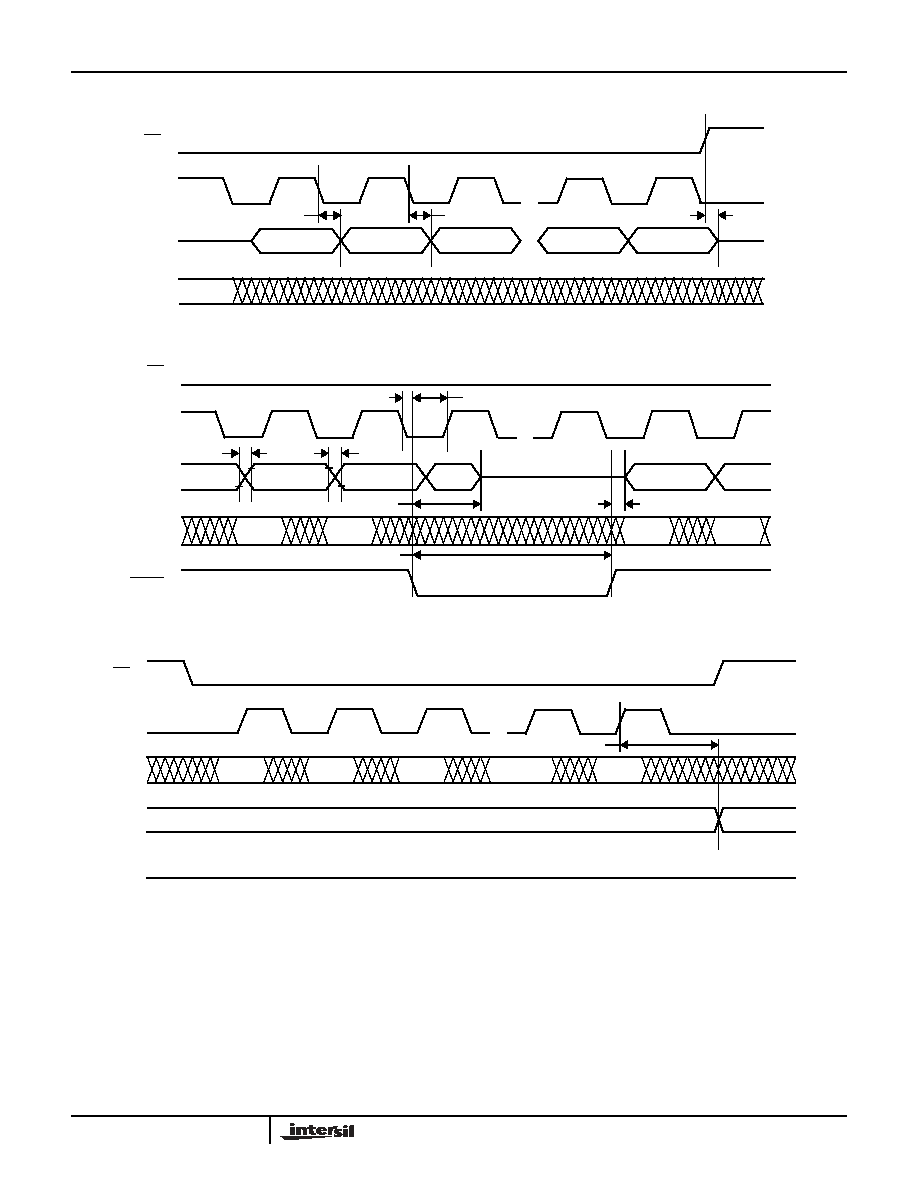
TIMING DIAGRAMS
Input Timing
Symbol
Parameter
Min. Max. Unit
t
WRPO
Wiper response time after the third (last) power supply is stable
10
Ķs
t
WRL
Wiper response time after instruction issued (all load instructions)
10
Ķs
t
WRID
Wiper response time from an active SCL/SCK edge (increment/decrement instruction)
10
Ķs
WAVEFORM
INPUTS
OUTPUTS
Must be
steady
Will be
steady
May change
from Low to
High
Will change
from Low to
High
May change
from High to
Low
Will change
from High to
Low
Don't Care:
Changes
Allowed
Changing:
State Not
Known
N/A
Center Line
is High
Impedance
...
CS
SCK
SI
SO
MSB
LSB
High Impedance
t
LEAD
t
H
t
SU
t
FI
t
CS
t
LAG
t
CYC
t
WL
...
t
RI
t
WH
X9430
15
FN8198.0
March 11, 2005
Output Timing
Hold Timing
DCP Timing (for All Load Instructions)
...
CS
SCK
SO
SI
ADDR
MSB
LSB
t
DIS
t
HO
t
V
...
...
CS
SCK
SO
SI
HOLD
t
HSU
t
HH
t
LZ
t
HZ
t
HOLD
t
RO
t
FO
...
CS
SCK
SI
MSB
LSB
VWx
t
WRL
...
SO
High Impedance
X9430

16
FN8198.0
March 11, 2005
DCP Timing (for Increment/Decrement Instruction)
Write Protect and Device Address Pins Timing
...
CS
SCK
SO
SI
ADDR
t
WRID
High Impedance
VWx
...
Inc/Dec
Inc/Dec
...
CS
WP
A0
A1
t
WPASU
t
WPAH
(Any Instruction)
X9430
17
FN8198.0
March 11, 2005
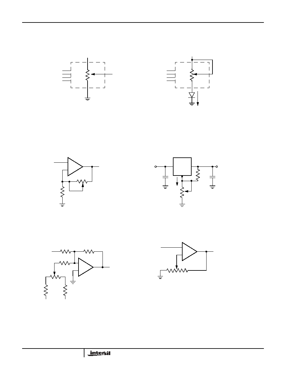
APPLICATIONS INFORMATION
Basic Configurations of Electronic Potentiometers
Application Circuits
V
R
V
W
+V
R
I
Three terminal Potentiometer;
Variable voltage divider
Two terminal Variable Resistor;
Variable current
Noninverting Amplifier
Voltage Regulator
Offset Voltage Adjustment
Comparator with Hysterisis
+
≠
V
S
V
O
R
2
R
1
V
O
= (1+R
2
/R
1
)V
S
R
1
R
2
I
adj
V
O
(REG) = 1.25V (1+R
2
/R
1
)+I
adj
R
2
V
O
(REG)
V
IN
317
+
≠
V
S
V
O
R
2
R
1
V
UL
= {R
1
/(R
1
+R
2
)} V
O
(max)
V
LL
= {R
1
/(R
1
+R
2
)} V
O
(min)
100k
10k
10k
10k
-12V
+12V
TL072
+
≠
V
S
V
O
R
2
R
1
}
}
X9430
18
FN8198.0
March 11, 2005
Application Circuits (continued)
Attenuator
Filter
Inverting Amplifier
Equivalent L-R Circuit
+
≠
V
S
V
O
R
3
R
1
V
O
= G V
S
-1/2
G
+1/2
G
O
= 1 + R
2
/R
1
fc = 1/(2
RC)
+
≠
V
S
V
O
R
2
R
1
Z
IN
= R
2
+ s R
2
(R
1
+ R
3
) C
1
= R
2
+ s Leq
(R
1
+ R
3
) >> R
2
+
≠
V
S
Function Generator
R
2
R
4
All R
S
= 10k
+
≠
V
S
R
2
R
1
R
C
}
}
V
O
= G V
S
G = - R
2
/R
1
R
2
C
1
R
1
R
3
Z
IN
+
≠
R
2
+
≠
R
1
}
}
R
A
R
B
frequency Ķ R
1
, R
2
, C
amplitude Ķ R
A
, R
B
C
V
O
X9430
19
FN8198.0
March 11, 2005
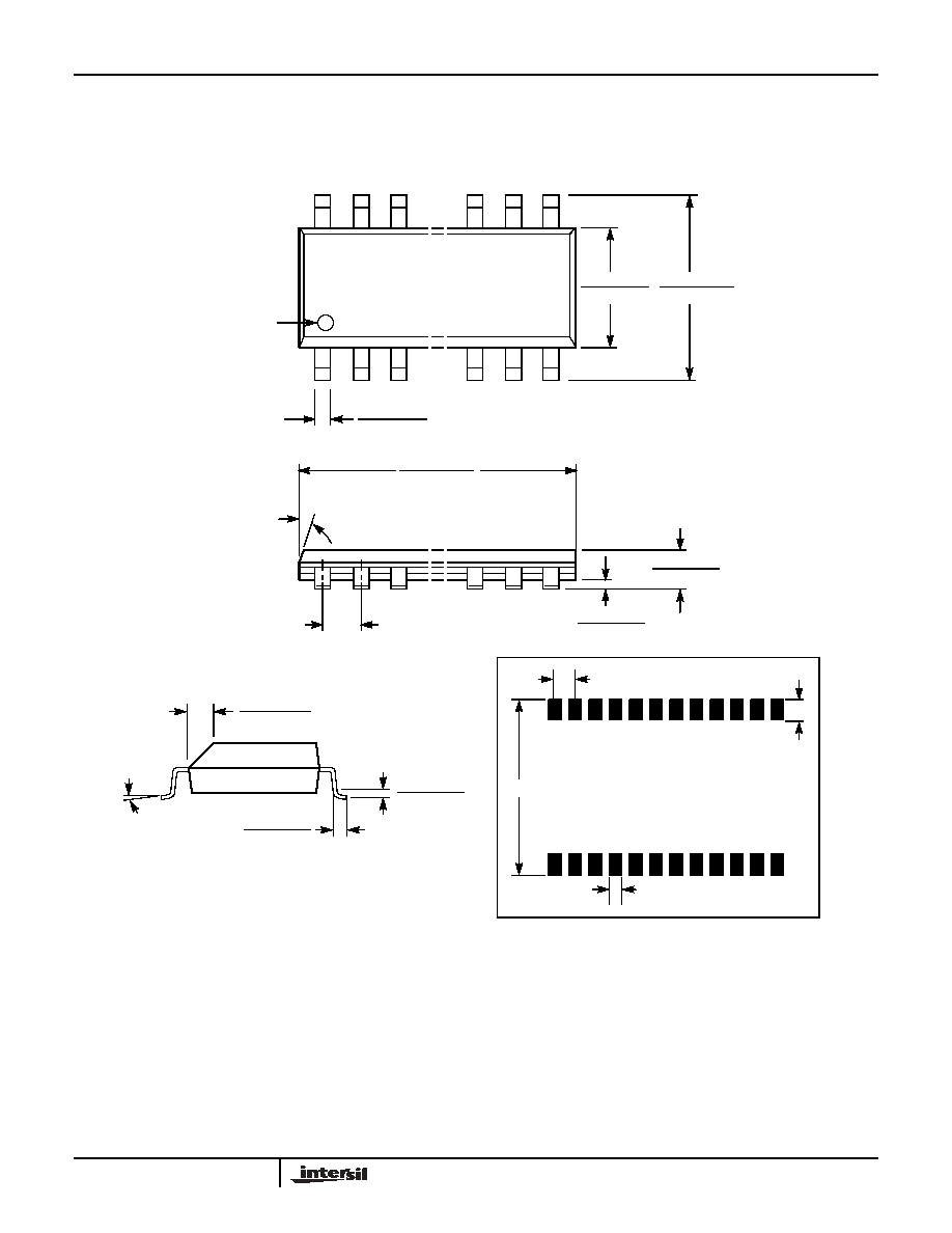
PACKAGING INFORMATION
0.290 (7.37)
0.299 (7.60)
0.393 (10.00)
0.420 (10.65)
0.014 (0.35)
0.020 (0.50)
Pin 1
Pin 1 Index
0.050 (1.27)
0.598 (15.20)
0.610 (15.49)
0.003 (0.10)
0.012 (0.30)
0.092 (2.35)
0.105 (2.65)
(4X) 7į
24-Lead Plastic Small Outline Gull Wing Package Type S
NOTE: ALL DIMENSIONS IN INCHES (IN PARENTHESES IN MILLIMETERS)
0.420"
0.050" Typical
0.050"
Typical
0.030" Typical
24 Places
FOOTPRINT
0.010 (0.25)
0.020 (0.50)
0.015 (0.40)
0.050 (1.27)
0.009 (0.22)
0.013 (0.33)
0į - 8į
X 45į
X9430
20
FN8198.0
March 11, 2005
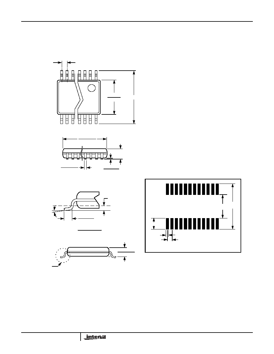
PACKAGING INFORMATION
NOTE: ALL DIMENSIONS IN INCHES (IN PARENTHESES IN MILLIMETERS)
24-Lead Plastic, TSSOP Package Type V
.169 (4.3)
.177 (4.5)
.252 (6.4) BSC
.026 (.65) BSC
.303 (7.70)
.311 (7.90)
.002 (.06)
.005 (.15)
.047 (1.20)
.0075 (.19)
.0118 (.30)
See Detail "A"
.031 (.80)
.041 (1.05)
.010 (.25)
.020 (.50)
.030 (.75)
Gage Plane
Seating Plane
Detail A (20X)
(4.16) (7.72)
(1.78)
(0.42)
(0.65)
ALL MEASUREMENTS ARE TYPICAL
0į - 8į
X9430
21
All Intersil U.S. products are manufactured, assembled and tested utilizing ISO9000 quality systems.
Intersil Corporation's quality certifications can be viewed at www.intersil.com/design/quality
Intersil products are sold by description only. Intersil Corporation reserves the right to make changes in circuit design, software and/or specifications at any time without
notice. Accordingly, the reader is cautioned to verify that data sheets are current before placing orders. Information furnished by Intersil is believed to be accurate and
reliable. However, no responsibility is assumed by Intersil or its subsidiaries for its use; nor for any infringements of patents or other rights of third parties which may result
from its use. No license is granted by implication or otherwise under any patent or patent rights of Intersil or its subsidiaries.
For information regarding Intersil Corporation and its products, see www.intersil.com
FN8198.0
March 11, 2005
Ordering Information
Device
V
CC
Limits
Blank = 5V Ī10%
-2.7 = 2.7 to 5.5V
Temperature Range
Blank = Commercial = 0 to +70įC
I = Industrial = -40 to +85įC
Package
S24 = 24-Lead SOIC
V24 = 24-Lead TSSOP
Potentiometer Organization
Pot 0
Pot 1
W =
10k
10k
X9430
P
T
V
Y
X9430