 | –≠–ª–µ–∫—Ç—Ä–æ–Ω–Ω—ã–π –∫–æ–º–ø–æ–Ω–µ–Ω—Ç: X9448YV24 | –°–∫–∞—á–∞—Ç—å:  PDF PDF  ZIP ZIP |
1
Æ
FN8201.0
CAUTION: These devices are sensitive to electrostatic discharge; follow proper IC Handling Procedures.
1-888-INTERSIL or 1-888-352-6832
|
Intersil (and design) is a registered trademark of Intersil Americas Inc.
XDCP is a trademark of Intersil Americas Inc. Copyright Intersil Americas Inc. 2005. All Rights Reserved
All other trademarks mentioned are the property of their respective owners.
X9448
Mixed Signal with 2-Wire Interface
Dual Digitally Controlled Potentiometer
(XDCPTM) & Voltage Comparator
FEATURES
∑ Two digitally controlled potentiometers and two
voltage comparators in one package
∑ 2-wire serial interface
∑ Register oriented format
--Direct read/write wiper position
--Store as many as four positions per pot
∑ Fast response comparator
∑ Enable, latch, or shutdown comparator outputs
through ACR
∑ Auto-recall of WCR and ACR data from R0
∑ Hardware write protection, WP
∑ Separate analog and digital/system supplies
∑ Direct write cell
--Endurance≠100,000 data changes per bit per
register
--Register data retention≠100 years
∑ 16-bytes of EEPROM memory
∑ Power saving feature and low noise
∑ Two 10k
or two 2.5k
potentiometers
∑ Resolution: 64 taps each pot
∑ 24-lead TSSOP and 24-lead SOIC packages
DESCRIPTION
The X9448 integrates two nonvolatile digitally con-
trolled potentiometers (XDCP) and two voltage com-
parators on a CMOS monolithic microcircuit.
The X9448 contains two resistor arrays, each com-
posed of 63 resistive elements. Between each ele-
ment and at either end are tap points accessible to the
wiper elements. The position of the wiper element on
the array is controlled by the user through the two wire
serial bus interface.
Each potentiometer has an associated voltage com-
parator. The comparator compares the external input
voltage V
NI
with the wiper voltage V
W
and sets the out-
put voltage level to a logic high or low.
Each resistor array and comparator has associated
with it a wiper counter register (WCR), analog control
register (ACR), and eight 6-bit data registers that can
be directly written and read by the user. The contents
of the wiper counter register controls the position of
the wiper on the resistor array. The contents of the
analog control register controls the comparator and its
output. The potentiometer is programmed with a
2-wire serial interface.
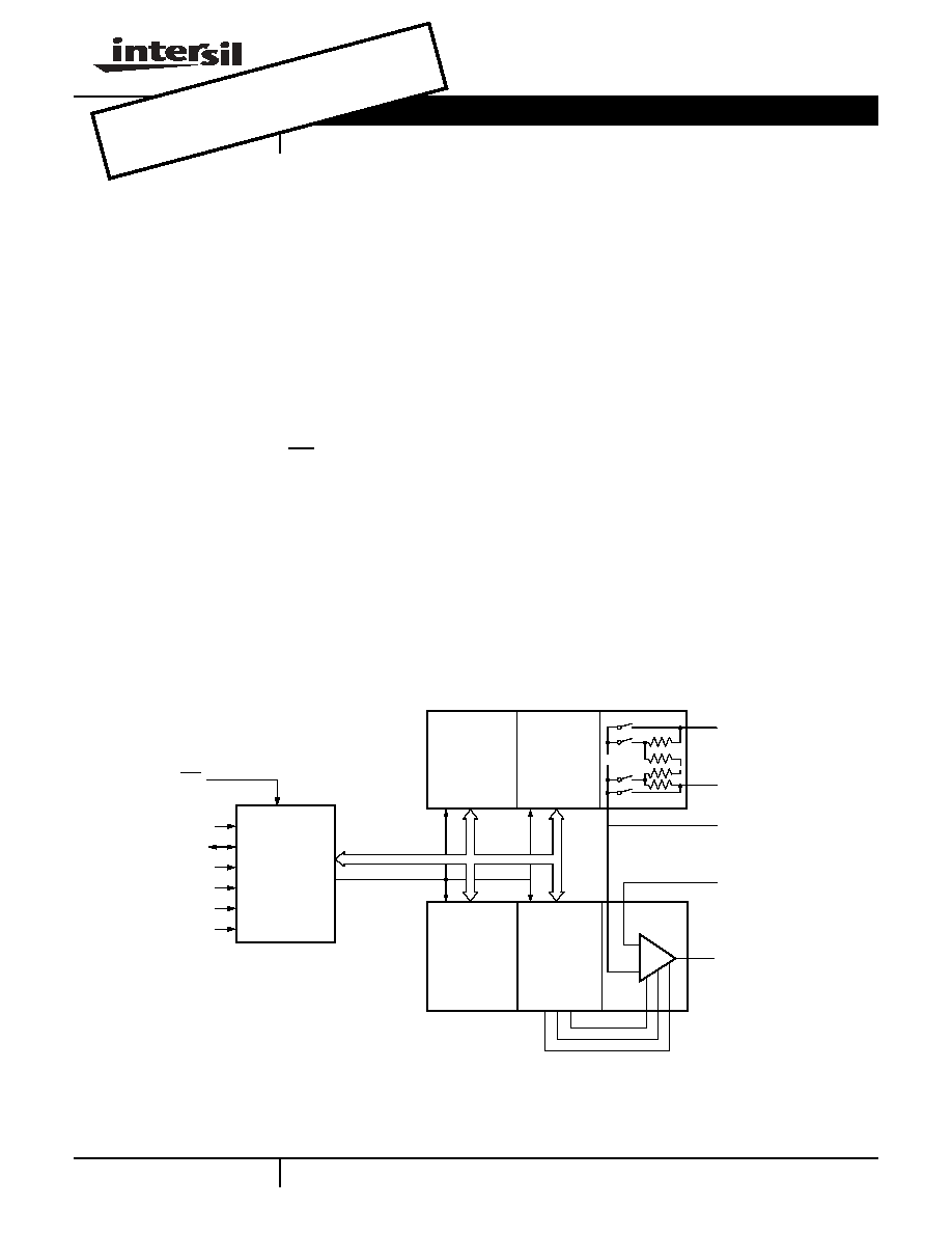
BLOCK DIAGRAM
V
OUT (0,1)
(R
0
-R
3
)
0,1
Interface
and
Control
Circuitry
SCL
SDA
A0
A1
A2
A3
V
H (0,1)
V
L (0,1)
WP
V
W (0,1)
V
NI (0,1)
+
≠
WCR
0,1
(R
0
-R
3
)
0,1
ACR
0,1
Data Sheet
April 18, 2005
OBSO
LETE
PRO
DUCT
POSS
IBLE
SUB
STITU
TE P
ROD
UCT
X941
8

2
FN8201.0
April 18, 2005
PIN DESCRIPTIONS
Host Interface Pins
Serial Clock (SCL)
The SCL input is used to clock data into and out of the
X9448.
Serial Data (SDA)
SDA is a bidirectional pin used to transfer data into
and out of the device. It is an open drain output and
may be wire-ORed with any number of open drain or
open collector outputs. An open drain output requires
the use of a pull-up resistor. For selecting typical val-
ues, refer to the guidelines for calculating typical val-
ues on the bus pull-up resistors graph.
Device Address (A
0
- A
3
)
The address inputs are used to set the least significant
4 bits of the 8-bit slave address. A match in the slave
address serial data stream must be made with the
address input in order to initiate communication with
the X9448. A maximum of 16 devices may share the
same 2-wire serial bus.
Potentiometer Pins
V
H
(V
H0
- V
H1
), V
L
(V
L0
- V
L1
)
The V
H
and V
L
inputs are equivalent to the terminal con-
nections on either end of a mechanical potentiometer.
V
W
(V
W0
- V
W1
)
The wiper output is equivalent to the wiper output of a
mechanical potentiometer and is connected to the
inverting input of the voltage comparator.
Comparator and Device Pins
Voltage Input V
NI0
, V
NI1
V
NI0
and V
NI1
are the input voltages to the plus (non-
inverting) inputs of the two comparators.
Buffered Voltage Outputs V
OUT0
, V
OUT1
The V
OUT0
, and V
OUT1
are the buffered voltage
comparator outputs enabled by respective bits in the
volatile analog control register.
Hardware Write Protect Input WP
The WP pin when low prevents nonvolatile writes to
the wiper counter and analog control registers.
Analog Supplies V+, V-
The analog supplies V+, V- are the supply voltages for
the XDCP analog section and the voltage comparators.
System Supply V
CC
and Ground V
SS
The system supply V
CC
and its reference V
SS
is used
to bias the interface and control circuits.
PIN CONFIGURATION
V
CC
V
L0
V
H0
WP
SDA
A1
1
2
3
4
5
6
7
8
9
10
24
23
22
21
20
19
18
17
16
V+
V
OUT0
V
NI0
NC
A0
NC
A
3
SCL
NC
V
NI1
SOIC
X9448
V
SS
V
W0
13
11
12
A
2
V
L1
V
H1
V
W1
V
OUT1
V
CC
V
L1
V
H1
WP
SDA
A
2
A
3
SCL
NC
V
NI1
TSSOP
V
SS
V
W1
A
1
V
L0
V
H0
V
W0
V-
V
OUT1
NC
V+
V
OUT0
V
NI0
A
0
NC
V-
15
14
1
2
3
4
5
6
7
8
9
10
24
23
22
21
20
19
18
17
16
X9448
13
11
12
15
14
X9448

3
FN8201.0
April 18, 2005
PIN NAMES
PRINCIPLES OF OPERATION
The X9448 is a highly integrated microcircuit incorpo-
rating two resistor arrays, two voltage comparators
and their associated registers and counters; and the
serial interface logic providing direct communication
between the host and the digitally-controlled potenti-
ometers and voltage comparators.
Serial Interface
The X9448 supports a bidirectional bus oriented proto-
col. The protocol defines any device that sends data
onto the bus as a transmitter and the receiving device
as the receiver. The device controlling the transfer is a
master and the device being controlled is the slave.
The master will always initiate data transfers and pro-
vide the clock for both transmit and receive operations.
Therefore, the X9448 will be considered a slave
device in all applications.
Clock and Data Conventions
Data states on the SDA line can change only during
SCL LOW periods (t
LOW
). SDA state changes during
SCL HIGH are reserved for indicating start and stop
conditions.
Start Condition
All commands to the X9448 are preceded by the start
condition, which is a HIGH to LOW transition of SDA
while SCL is HIGH (t
HIGH
). The X9448 continuously
monitors the SDA and SCL lines for the start condition
and will not respond to any command until this condi-
tion is met.
Stop Condition
All communications must be terminated by a stop con-
dition, which is a LOW to HIGH transition of SDA while
SCL is HIGH.
Acknowledge
Acknowledge is a software convention used to provide
a positive handshake between the master and slave
devices on the bus to indicate the successful receipt of
data. The transmitting device, either the master or the
slave, will release the SDA bus after transmitting eight
bits. The master generates a ninth clock cycle and
during this period the receiver pulls the SDA line LOW
to acknowledge that it successfully received the eight
bits of data.
The X9448 will respond with an acknowledge after
recognition of a start condition and its slave address
and once again after successful receipt of the com-
mand byte. If the command is followed by a data byte
the X9448 will respond with a final acknowledge.
Array Description
The X9448 is comprised of two resistor arrays and
two voltage comparators. Each array contains 63 dis-
crete resistive segments that are connected in series.
The physical ends of each array are equivalent to the
fixed terminals of a mechanical potentiometer (V
H
and V
L
inputs).
At both ends of each array and between each resistor
segment is a CMOS switch connected to the wiper
(V
W
) output. Within each individual array only one
switch may be turned on at a time. These switches are
controlled by a volatile wiper counter register (WCR).
The six bits of the WCR are decoded to select, and
enable, one of sixty-four switches.
The WCR may be written directly, or it can be changed
by transferring the contents of one of four associated
data registers into the WCR. These data registers and
the WCR can be read and written by the host system.
Symbol
Description
SCL
Serial Clock
SDA
Serial Data
A0 - A3
Device Address
V
H0
- V
H1
,
V
L0
- V
L1
Potentiometers (terminal equivalent)
V
W0
- V
W1
Potentiometers (wiper equivalent)
V
NI0
, V
NI1
Comparator Input Voltages
V
OUT0,
V
OUT1
Buffered Comparator Outputs
WP
Hardware Write Protection
V+,V-
Analog and Voltage Comparator
Supplies
V
CC
System/Digital Supply Voltage
V
SS
System Ground
NC
No Connection
X9448

4
FN8201.0
April 18, 2005
Voltage Comparator
The comparator compares the wiper voltage V
W
with
the external input voltage V
NI
. The comparator and its
logic level output are controlled by the Shutdown,
Latch, and Enable bits of the analog control register
(ACR). Enable connects the comparator output to the
V
OUT
pin, Latch memorizes the output logic state, and
Shutdown removes the analog section supply voltages
to save power. The analog control register is pro-
grammed using the two wire serial interface.
The ACR may be written directly, or it can be changed
by transferring the contents of one of four associated
data registers into the ACR. These data registers and
the ACR may be read and written by the host system.
INSTRUCTIONS AND PROGRAMMING
Device Addressing
Following a start condition the master must output the
address of the slave it is accessing. The most signifi-
cant four bits of the slave address are the device type
identifier (refer to Figure 1 below). For the X9448 this
is fixed as 0101[B].
Figure 1. Address/Identification Byte Format
The next four bits of the slave address are the device
address. The physical device address is defined by
the state of the A0 - A3 inputs. The X9448 compares
the serial data stream with the address input state; a
successful compare of all four address bits is required
for the X9448 to respond with an acknowledge. The
A
0
- A
3
inputs can be actively driven by CMOS input
signals or tied to V
CC
or V
SS
.
Acknowledge Polling
The disabling of the inputs, during the internal nonvol-
atile write operation, can be used to take advantage of
the typical 5ms EEPROM write cycle time. Once the
stop condition is issued to indicate the end of the non-
volatile write command the X9448 initiates the internal
write cycle. ACK polling (Flow 1) can be initiated
immediately. This involves issuing the start condition
followed by the device slave address. If the X9448 is
still busy with the write operation no ACK will be
returned. If the X9448 has completed the write opera-
tion an ACK will be returned and the master can then
proceed with the next operation.
Flow 1. ACK Polling Sequence
Instruction Structure
The byte following the address contains the instruction
and register pointer information. The four most signifi-
cant bits are the instruction. The next four bits point to
one of two pots or one of two voltage comparators and
when applicable they point to one of four associated
registers. The format is shown below in Figure 2.
Figure 2. Instruction Byte Format
The four high order bits define the instruction. The
next two bits (R1 and R0) select one of the four regis-
ters that is to be acted upon when a register oriented
instruction is issued. The last two bits (P1 and P0)
select which one of the two potentiometers or which
one of the two voltage comparators is to be affected by
the instruction.
Four of the nine instructions end with the transmission
of the instruction byte. The basic sequence is illus-
trated in Figure 3. These two-byte instructions
exchange data between the wiper counter register or
analog control register and one of the data registers. A
transfer from a data register to a wiper counter register
1
0
0
A3
A2
A1
A0
Device Type
Identifier
Device Address
1
Nonvolatile Write
Command Completed
Enter ACK Polling
Issue
START
Issue Slave
Address
ACK
Returned?
Further
Operation
Issue
Instruction
PROCEED
Issue STOP
NO
YES
YES
PROCEED
Issue STOP
NO
I1
I2
I3
I0
R1
R0
P1
P0
WCR and ACR Select
Register
Select
Instructions
X9448

5
FN8201.0
April 18, 2005
or analog control register is essentially a write to a
static RAM. The response of the wiper to this action
will be delayed t
STPWV
. A transfer from the Wiper
Counter Register current wiper position to a data reg-
ister is a write to nonvolatile memory and takes a mini-
mum of t
WR
to complete. The transfer can occur
between one of the two potentiometers or one of the
two voltage comparators and one of its associated
registers; or it may occur globally, wherein the transfer
occurs between both of the potentiometers and volt-
age comparators and one of their associated registers.
Four instructions require a three-byte sequence to com-
plete. The basic sequence is illustrated in Figure 4.
These instructions transfer data between the host and
the X9448; either between the host and one of the data
registers or directly between the host and the wiper
counter and analog control registers. These instructions
are: read wiper counter register or analog control regis-
ter, read the current wiper position of the selected pot or
the comparator control bits, Write wiper counter register
or analog control register, i.e. change current wiper
position of the selected pot or control the voltage com-
parator; read data register, read the contents of the
selected nonvolatile register; write data register, write a
new value to the selected data register. The bit struc-
tures of the instructions are shown in Figure 6.
The increment/decrement command is different from
the other commands. Once the command is issued
and the X9448 has responded with an acknowledge,
the master can clock the selected wiper up and/or
down in one segment steps; thereby, providing a fine
tuning capability to the host. For each SCL clock pulse
(t
HIGH
) while SDA is HIGH, the selected wiper will
move one resistor segment towards the V
H
terminal.
Similarly, for each SCL clock pulse while SDA is LOW,
the selected wiper will move one resistor segment
towards the V
L
terminal. A detailed illustration of the
sequence for this operation is shown in Figure 5.
Figure 3. Two-Byte Command Sequence
Figure 4. Three-Byte Command Sequence
Figure 5. Increment/Decrement Command Sequence
S
T
A
R
T
0
1
0
1
A3 A2 A1 A0
A
C
K
I3
I2
I1
I0
R1 R0 P1 P0
A
C
K
SCL
SDA
S
T
O
P
S
T
A
R
T
0
1
0
1
A3 A2 A1 A0 A
C
K
I3
I2
I1 I0
P1 P0 R1 R0 A
C
K
SCL
SDA
S
T
O
P
A
C
K
D5 D4 D3 D2 D1 D0
S
T
A
R
T
0
1
0
1
A3 A2 A1 A0
A
C
K
I3
I2
I1
I0
P1 P0 R1 R0 A
C
K
SCL
SDA
S
T
O
P
X
X
I
N
C
1
I
N
C
2
I
N
C
n
D
E
C
1
D
E
C
n
X9448

6
FN8201.0
April 18, 2005
Figure 6. Instruction Set
Read Wiper Counter Register (WCR) or Analog Control Register (ACR)
Read the contents of the Wiper Counter Register or Analog Control Register pointed to by P
1
- P
0
.
P1 P0: 00 - WCR0, 01 - WCR1
P1 P0: 10 - ACR0, 11 - ACR1
Write Wiper Counter Register (WCR) or Analog Control Register (ACR)
Write new value to the Wiper Counter Register or Analog Control Register pointed to by P
1
- P
0
.
P1 P0: 00 - WCR0, 01 - WCR1
P1 P0: 10 - ACR0, 11 - ACR1
Read Data Register (DR)
Read the contents of the Register pointed to by P
1
- P
0
and R
1
- R
0
.
R1 R0: 00 - R0, 10 - R1
01 - R2,11 - R3
Definitions:
SACK ≠ Slave acknowledge, MACK ≠ Master acknowledge, I/O ≠ Increment/Decrement (I/O), R ≠ Register,
P ≠ Potentiometer
S
T
A
R
T
device type
identifier
device
addresses
S
A
C
K
instruction
opcode
WCR/ACR
addresses
S
A
C
K
register data
(sent by slave on SDA)
M
A
C
K
S
T
O
P
0 1 0 1 A
3
A
2
A
1
A
0
1 0 0 1 0 0 P
1
P
0
0 0 D
5
D
4
D
3
D
2
D
1
D
0
S
T
A
R
T
device type
identifier
device
addresses
S
A
C
K
instruction
opcode
WCR/ACR
addresses
S
A
C
K
register data
(sent by master on SDA)
S
A
C
K
S
T
O
P
0 1 0 1 A
3
A
2
A
1
A
0
1 0 1 0 0 0 P
1
P
0
0 0 D
5
D
4
D
3
D
2
D
1
D
0
S
T
A
R
T
device type
identifier
device
addresses
S
A
C
K
instruction
opcode
WCR/ACR/DR
addresses
S
A
C
K
register data
(sent by master on SDA)
M
A
C
K
S
T
O
P
0 1 0 1 A
3
A
2
A
1
A
0
1 0 1 1 R
1
R
0
P
1
P
0
0 0 D
5
D
4
D
3
D
2
D
1
D
0
X9448

7
FN8201.0
April 18, 2005
Write Data Register (DR)
Write new value to the Register pointed to by P
1
- P
0
and R
1
- R
0
.
Transfer Data Register to Wiper Counter Register or Analog Control Register
Transfer the contents of the Register pointed to by R
1
- R
0
to the WCR or ACR pointed to by P
1
- P
0
.
Transfer Wiper Counter or Analog Control Register to Data Register
Transfer the contents of the WCR or ACR pointed to by P
1
- P
0
to the Register pointed to by R
1
- R
0
.
Global Transfer Data Register to Wiper Counter or Analog Control Register
Transfer the contents of all four Data Registers pointed to by R
1
- R
0
to their respective WCR or ACR.
Global Transfer Wiper Counter or Analog Control Register to Data Register
Transfer the contents of all WCRs and ACRs to their respective data Registers pointed to by R
1
- R
0
.
Increment/Decrement Wiper Counter Register
Enable Increment/decrement of the WCR pointed to by P
1
- P
0
.
P1 P0: 00 or 01 only.
S
T
A
R
T
device type
identifier
device
addresses
S
A
C
K
instruction
opcode
WCR/ACR/DR
addresses
S
A
C
K
register data
(sent by master on SDA)
S
A
C
K
S
T
O
P
HIGH-VOLTAGE
WRITE CYCLE
0 1 0 1 A
3
A
2
A
1
A
0
1 1 0 0 R
1
R
0
P
1
P
0
0 0 D
5
D
4
D
3
D
2
D
1
D
0
S
T
A
R
T
device type
identifier
device
addresses
S
A
C
K
instruction
opcode
WCR/ACR/DR
addresses
S
A
C
K
S
T
O
P
0 1 0 1 A
3
A
2
A
1
A
0
1 1 0 1 R
1
R
0
P
1
P
0
S
T
A
R
T
device type
identifier
device
addresses
S
A
C
K
instruction
opcode
WCR/ACR/DR
addresses
S
A
C
K
S
T
O
P
HIGH-VOLTAGE
WRITE CYCLE
0 1 0 1 A
3
A
2
A
1
A
0
1 1 1 0 R
1
R
0
P
1
P
0
S
T
A
R
T
device type
identifier
device
addresses
S
A
C
K
instruction
opcode
DR
addresses
S
A
C
K
S
T
O
P
0 1 0 1 A
3
A
2
A
1
A
0
0 0 0 1 R
1
R
0 0 0
S
T
A
R
T
device type
identifier
device
addresses
S
A
C
K
instruction
opcode
DR
addresses
S
A
C
K
S
T
O
P
HIGH-VOLTAGE
WRITE CYCLE
0 1 0 1 A
3
A
2
A
1
A
0
1 0 0 0 R
1
R
0 0 0
S
T
A
R
T
device type
identifier
device
addresses
S
A
C
K
instruction
opcode
WCR
addresses
S
A
C
K
increment/decrement
(sent by master on SDA)
S
T
O
P
0 1 0 1 A
3
A
2
A
1
A
0
0 0 1 0 0 0 P
1
P
0
I/
D
I/
D .
.
.
. I/
D
I/
D
X9448
8
FN8201.0
April 18, 2005
REGISTERS OPERATION
Both XDCP potentiometers and voltage comparators
share the serial interface and share a common archi-
tecture. Each potentiometer and voltage comparator is
associated with wiper counter and analog control reg-
isters and eight data registers. A detailed discussion of
the register organization and array operation follows.
Wiper Counter (WCR) and Analog Control
Registers (ACR)
The X9448 contains two wiper counter registers one
for each XDCP potentiometer and two analog control
registers, one for each of the two voltage comparators.
The wiper counter register is equivalent to a serial-in,
parallel-out counter with its outputs decoded to select
one of sixty-four switches along its resistor array. The
contents of the wiper counter register and analog con-
trol register can be altered in four ways: it may be writ-
ten directly by the host via the Write WCR instruction
(serial load); it may be written indirectly by transferring
the contents of one of four associated data registers
(DR) via the XFR data register instruction (parallel
load); it can be modified one step at a time by the
increment/decrement instruction (WCR only). Finally,
it is loaded with the contents of its data register zero
(R0) upon power-up.
The wiper counter and analog control register are vol-
atile registers; that is, their contents are lost when the
X9448 is powered-down. Although the registers are
automatically loaded with the value in R0 upon power-
up, it should be noted this may be different from the
value present at power-down.
Programming the ACR is similar to the WCR. How-
ever, the 6 bits in the WCR positions the wiper in the
resistor array while 3 bits in the ACR control the com-
parator and its output.
Data Registers (DR)
Each potentiometer and each voltage comparator has
four nonvolatile data registers (DR). These can be
read or written directly by the host and data can be
transferred between any of the four data registers and
the WCR or ACR. It should be noted all operations
changing data in one of these registers is a nonvolatile
operation and will take a maximum of 10ms.
If the application does not require storage of multiple
settings for the potentiometer or comparator, these
registers can be used as regular memory locations that
could store system parameters or user preference data.
REGISTER DESCRIPTIONS
Wiper Counter Register (WCR)
WP0-WP5 identify wiper position.
Analog Control Register (ACR)
Shutdown
"1"
indicates power is connected to the voltage
comparator.
"0"
indicates power is not connected to the voltage
comparator.
Enable
"1"
indicates the output buffer of the voltage com-
parator is enabled.
"0"
indicates the output buffer of the voltage com-
parator is disabled.
Latch
"1"
indicates the output of the voltage comparator
is memorized or latched.
"0"
indicates the output of the voltage comparator
is not latched.
Userbits--available for user applications
Data Registers (DR, R0 - R3)
Memory Map
0
0
WP5 WP4 WP3 WP2 WP1 WP0
(volatile)
(LSB)
0
0
User
-bit5
User
-bit4
User
-bit3 Latch Enable
Shut-
down
(volatile)
(LSB)
Wiper Position or Analog Control Data or User Data
(Nonvolatile)
WCRO
WCR1
ACR0
ACR1
R0
R0
R0
R0
R1
R1
R1
R1
R2
R2
R2
R2
R3
R3
R3
R3
X9448
9
FN8201.0
April 18, 2005
ABSOLUTE MAXIMUM RATINGS
Temperature under bias .................... -65∞C to +135∞C
Storage temperature ......................... -65∞C to +150∞C
Voltage on SDA, SCL or any
address input with respect to V
SS
........... -1V to +7V
Voltage on any V+ (referenced to V
SS
) ................
+
7V
Voltage on any V- (referenced to V
SS
) .................. -7V
(V+) - (V-) ............................................................. 10V
Any V
H
.....................................................................V+
Any V
L
......................................................................V-
Lead temperature (soldering, 10 seconds)........ 300∞C
COMMENT
Stresses above those listed under "Absolute Maximum
Ratings" may cause permanent damage to the device.
This is a stress rating only; functional operation of the
device (at these or any other conditions above those
listed in the operational sections of this specification) is
not implied. Exposure to absolute maximum rating con-
ditions for extended periods may affect device reliability.
POTENTIOMETER CHARACTERISTICS (Over recommended operating conditions unless otherwise stated.)
Notes: (1) Absolute linearity is utilized to determine actual wiper voltage versus expected voltage as determined by wiper position when used
as a potentiometer.
(2) Relative linearity is utilized to determine the actual change in voltage between two successive tap positions when used as a
potentiometer. It is a measure of the error in step size.
(3) MI = RTOT/63 or (V
H
- V
L
)/63, single pot.
(4) Individual array resolutions.
Symbol
Parameter
Limits
Test Conditions
Min.
Typ.
Max.
Unit
R
TOTAL
End to end resistance
-20
+20
%
Power rating
50
mW
25∞C, each pot
I
W
Wiper current
-3
+3
mA
R
W
Wiper resistance
40
100
V
CC
= 5V, Wiper Current = 3mA
100
250
V
CC
= 2.7-5V, Wiper Current = 3mA
Vv+
Voltage on V+ Pin
X9440
+4.5
+5.5
V
X9440-2.7
+2.7
+5.5
Vv-
Voltage on V- Pin
X9440
-5.5
-4.5
V
X9440-2.7
-5.5
-2.7
V
TERM
Voltage on any V
H
or V
L
pin
V-
V+
V
Noise
-120
dBv
Ref: 1V
Resolution
(4)
1.6
%
Absolute linearity
(1)
-1
+1
MI
(3)
V
w(n)(actual)
- V
w(n)(expected)
Relative linearity
(2)
-0.2
+0.2
MI
(3)
V
w(n + 1)
- [V
w(n) + MI
]
Temperature Coefficient of R
TOTAL
±
300
ppm/∞C
RECOMMENDED OPERATING CONDITIONS
Temperature
Min.
Max.
Commercial
0
∞C
+70
∞C
Industrial
-40
∞C
+85
∞C
Military
-55∞C
+125∞C
Device
Supply Voltage (V
CC
) Limits
X9448
5V
±
10%
X9448-2.7
2.7V to 5.5V
X9448

10
FN8201.0
April 18, 2005
COMPARATOR ELECTRICAL CHARACTERISTICS
(Over the recommended operating conditions unless otherwise specified.)
Notes: (1) 100mV step with 100mV overdrive, ZL = 10k
|| 15pF, 10-90% risetime.
(2) Time from leading edge of enable bit to valid V
OUT
.
SYSTEM/DIGITAL D.C. OPERATING CHARACTERISTICS
(Over the recommended operating conditions unless otherwise specified.)l
ENDURANCE AND DATA RETENTION
Symbol
Parameter
Limits
Unit
Test Conditions
Min.
Typ.
Max.
V
OS
Input offset voltage
-1
-5
1
5
mV
mV
V+/V- =
±
3V
V+/V- =
±
5V
I
B
Input current
10
pA
V
IR
Input voltage range
V-
V+
V
t
R
Response time
200
ns
note 1
I
O
Output current
-1
1
mA
A
V
Voltage gain
V/mV
PSRR
Power supply rejection ratio
60
dB
V
OR
Output voltage range
V
SS
V
CC
V
T
C
V
OS
Input offset voltage drift
6
µV/∞C
I
S
Supply current (V+ to V-)
1.2
.5
mA
mA
V+/V- =
±
5V
V+/V- =
±
3V
T
ON
Comparator enable time
1
µs
note 2
V
OL
Output low voltage
0.4
V
I
O
= 1mA
V
OH
Output high voltage
V
CC
- 0.8
V
I
O
= 1mA
Symbol
Parameter
Limits
Test Conditions
Min.
Typ.
Max.
Unit
I
CC
V
CC
supply current (active)
400
µA
f
SCL
= 400kHz, SDA = Open,
Other Inputs = V
SS
I
SB
V
CC
current (standby)
1
µA
SCL = SDA = V
CC
, Addr. = V
SS
I
LI
Input leakage current
10
µA
V
IN
= V
SS
to V
CC
I
LO
Output leakage current
10
µA
V
OUT
= V
SS
to V
CC
V
IH
Input HIGH voltage
V
CC
x 0.7
V
CC
+ 0.5
V
V
IL
Input LOW voltage
-0.5
V
CC
x 0.1
V
V
OL
Output LOW voltage
0.4
V
I
OL
= 3mA
Parameter
Min.
Unit
Minimum endurance
100,000
Data changes per bit per register
Data retention
100
Years
X9448
11
FN8201.0
April 18, 2005
CAPACITANCE
Power-Up Timing and Sequence
A.C. TEST CONDITIONS
Note:
(1) Applicable to recall and power consumption applica-
tions
EQUIVALENT A.C. LOAD CIRCUIT
TIMING DIAGRAMS
START and STOP Timing
Input Timing
Symbol
Test
Typical
Unit
Test Conditions
C
I/O
Input/output capacitance (SDA)
8
pF
V
I/O
= 0V
C
IN
Input capacitance (A0, A1, A2, A3, and SCL)
6
pF
V
IN
= 0V
C
L
, C
H
, C
W
Potentiometer capacitance
10/10/25
pF
Power-up sequence
(1)
: (1) V
CC
(2) V+ and V- {V+
V
CC
at all times}
Power-down sequence: no limitation
Input pulse levels
V
CC
x 0.1 to V
CC
x 0.9
Input rise and fall times
10ns
Input and output timing level
V
CC
x 0.5
5V
1533
100pF
SD Output
2.7V
100pF
t
SU:STA
t
HD:STA
t
SU:STO
SCL
SDA
t
R
(START)
(STOP)
t
F
t
R
t
F
SCL
SDA
t
HIGH
t
LOW
t
CYC
t
HD:DAT
t
SU:DAT
t
BUF
X9448
12
FN8201.0
April 18, 2005
Output Timing
XDCP Timing (for All Load Instructions)
XDCP Timing (for Increment/Decrement Instruction)
Write Protect and Device Address Pins Timing
SCL
SDA
t
DH
t
AA
SCL
SDA
VWx
(STOP)
LSB
t
WRL
SCL
SDA
VWx
t
WRID
Wiper Register Address
Inc/Dec
Inc/Dec
SDA
SCL
...
...
...
WP
A0, A1
A2, A3
t
SU:WPA
t
HD:WPA
(START)
(STOP)
(Any Instruction)
X9448
13
FN8201.0
April 18, 2005
AC Timing
High-Voltage Write Cycle Timing
XDCP Timing
Note:
(4) V
CC
= 5V/2.7V
Symbol
Parameter
Min.
Max.
Unit
f
SCL
Clock frequency
400
kHz
t
CYC
Clock cycle time
2500
ns
t
HIGH
Clock high time
600
ns
t
LOW
Clock low time
1300
ns
t
SU:STA
Start setup time
600
ns
t
HD:STA
Start hold time
600
ns
t
SU:STO
Stop setup time
600
ns
t
SU:DAT
SDA data input setup time
100
ns
t
HD:DAT
(4)
SDA data input hold time
0/30
ns
t
R
SCL and SDA rise time
300
ns
t
F
SCL and SDA fall time
300
ns
t
AA
SCL low to SDA data output valid time
100
900
ns
t
DH
SDA Data output hold time
50
ns
T
I
Noise suppression time constant at SCL and SDA inputs
50
ns
t
BUF
Bus free time (prior to any transmission)
1300
ns
t
SU:WPA
WP, A0, A1, A2 and A3 setup time
0
ns
t
HD:WPA
WP, A0, A1, A2 and A3 hold time
0
ns
Symbol
Parameter
Typ.
Max.
Unit
t
WR
High-voltage write cycle time (store instructions)
5
10
ms
Symbol
Parameter
Min.
Max.
Unit
t
WRL
Wiper response time after instruction issued (all load instructions)
10
µs
X9448
14
FN8201.0
April 18, 2005
BASIC APPLICATIONS
Programmable Level Detector with Memory (typical bias conditions)
+5V
V
H
V+
SCL
SDA
V
OUT
≠
+
V≠
V
L
V
SS
SCL
SDA
9448
V
REF1
(+5V)
V
TRANSDUCER
(V
T
)
V
W
V
OUT
Programmable Window Detector with Memory
SCL
+
≠
SDA
+
≠
+5V
-5V
9448
V
W0
V
W1
V
OUT0
V
OUT1
V
OUT0
V
S
V
LL
V
UL
(V
W1
)
(V
W0
)
V
T
>V
W
, V
OUT
= High
V
T
<V
W
, V
OUT
= Low
+
≠
V
OUT0
= L
V
OUT1
= L
V
OUT0
= H
V
OUT1
= H
V
OUT0
= L
V
OUT1
= H
For the signal voltage
V
S
> the upper limit V
UL
, (V
OUT0
= H) ∑ (V
OUT1
= H)
V
S
< the lower limit V
LL
, (V
OUT0
= L) ∑ (V
OUT1
= L)
For the window V
LL
V
S
V
UL
, (V
OUT0
= L) ∑ (V
OUT1
= H)
V
S
+
≠
V
CC
V
NI
(+5V)
(-5V)
V
REF2
(-5V)
X9448

15
FN8201.0
April 18, 2005
BASIC APPLICATION (continued)
Programmable Oscillator with Memory
Programmable Schmitt Trigger with Memory
+5V
V
H
V+
SCL
SDA
≠
+
V≠
V
W
V
OUT
Frequency µ R, C
V
L
+5V
R
2
R
1
R
3
R
C
Duty Cycle µ R
1
, R
2
, R
3
V
H
V+
≠
+
V≠
V
OUT
V
L
R
2
R
1
R
V
S
V
LL
V
UL
V
OUT
V
LL
R
1
R
2
+
R
2
---------------------V
W
R
1
R
2
-------V
OUT
max
(
)
≠
=
V
UL
R
1
R
2
+
R
2
---------------------V
W
R
1
R
2
-------V
OUT
min
(
)
≠
=
V
R
V
W
V
S
9448
9448
X9448
16
FN8201.0
April 18, 2005
BASIC APPLICATION (continued)
Programmable Level Detector (alternate technique)
Programmable Time Delay with Memory
≠
+
V
R
V
OUT
+
+
R
2
{
{
R
1
V
S
V
OUT
High for V
S
≠
R
1
R
2
-------V
R
<
=
V
OUT
Low for V
S
≠
R
1
R
2
-------V
R
>
=
R
1
R
2
+
R
POT
=
V
OUT
V
S
-R
1
R
2
V
R
V
H
≠
+
V
L
V
W
V
OUT
V
NI
V
OUT
Dt
+5V
V
S
R
C
t
RC
ln
5V
5V V
W
≠
(
)
-------------------------
=
t
t
t
+5v
+5v
+5v
V
S
V
NI
V
OUT
V
W
V
CC
V
SS
X9448
17
FN8201.0
April 18, 2005
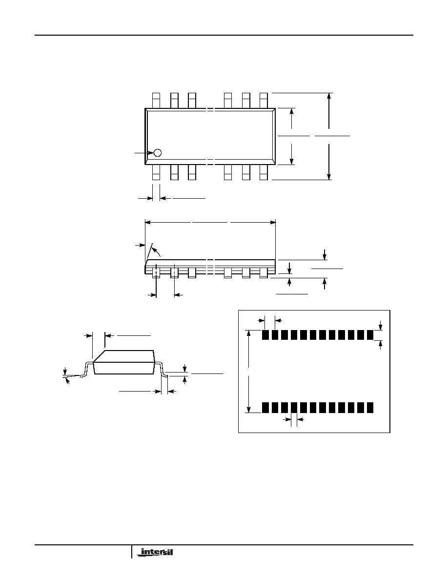
PACKAGING INFORMATION
0.290 (7.37)
0.299 (7.60)
0.393 (10.00)
0.420 (10.65)
0.014 (0.35)
0.020 (0.50)
Pin 1
Pin 1 Index
0.050 (1.27)
0.598 (15.20)
0.610 (15.49)
0.003 (0.10)
0.012 (0.30)
0.092 (2.35)
0.105 (2.65)
(4X) 7∞
24-Lead Plastic Small Outline Gull Wing Package Type S
NOTE: ALL DIMENSIONS IN INCHES (IN PARENTHESES IN MILLIMETERS)
0.420"
0.050" Typical
0.050"
Typical
0.030" Typical
24 Places
FOOTPRINT
0.010 (0.25)
0.020 (0.50)
0.015 (0.40)
0.050 (1.27)
0.009 (0.22)
0.013 (0.33)
0∞ - 8∞
X 45∞
X9448

18
FN8201.0
April 18, 2005
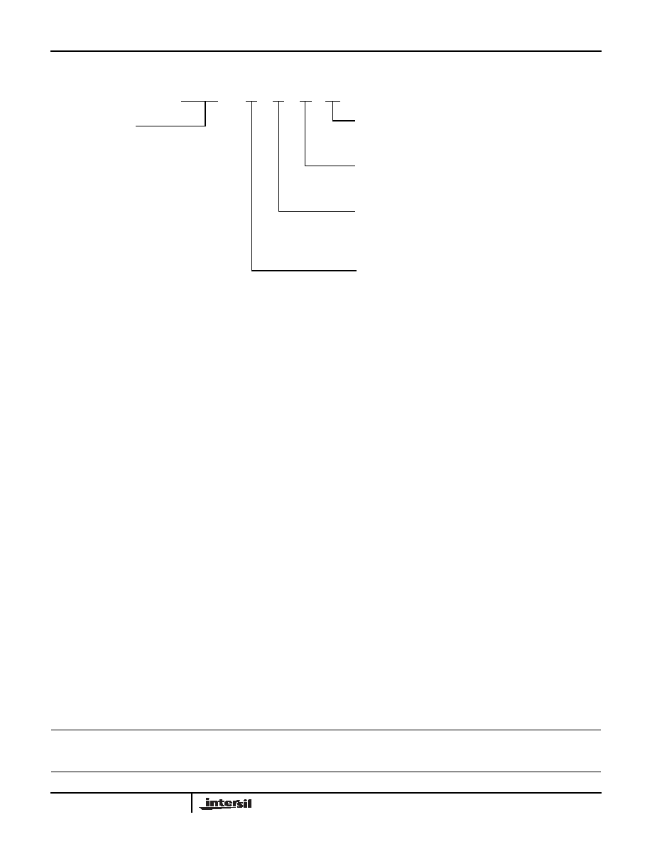
PACKAGING INFORMATION
NOTE: ALL DIMENSIONS IN INCHES (IN PARENTHESES IN MILLIMETERS)
24-Lead Plastic, TSSOP Package Type V
.169 (4.3)
.177 (4.5)
.252 (6.4) BSC
.026 (.65) BSC
.303 (7.70)
.311 (7.90)
.002 (.06)
.005 (.15)
.047 (1.20)
.0075 (.19)
.0118 (.30)
See Detail "A"
.031 (.80)
.041 (1.05)
.010 (.25)
.020 (.50)
.030 (.75)
Gage Plane
Seating Plane
Detail A (20X)
(4.16) (7.72)
(1.78)
(0.42)
(0.65)
ALL MEASUREMENTS ARE TYPICAL
0∞ - 8∞
X9448
19
All Intersil U.S. products are manufactured, assembled and tested utilizing ISO9000 quality systems.
Intersil Corporation's quality certifications can be viewed at www.intersil.com/design/quality
Intersil products are sold by description only. Intersil Corporation reserves the right to make changes in circuit design, software and/or specifications at any time without
notice. Accordingly, the reader is cautioned to verify that data sheets are current before placing orders. Information furnished by Intersil is believed to be accurate and
reliable. However, no responsibility is assumed by Intersil or its subsidiaries for its use; nor for any infringements of patents or other rights of third parties which may result
from its use. No license is granted by implication or otherwise under any patent or patent rights of Intersil or its subsidiaries.
For information regarding Intersil Corporation and its products, see www.intersil.com
FN8201.0
April 18, 2005
ORDERING INFORMATION
Device
V
CC
Limits
Blank = 5V
±
10%
-2.7 = 2.7 to 5.5V
Temperature Range
Blank = Commercial = 0
∞
C to +70
∞
C
I = Industrial = -40
∞
C to +85
∞
C
Package
P24 = 24-Lead Plastic DIP
S24 = 24-Lead SOIC
V24 = 24-Lead TSSOP
Potentiometer Organization
Pot 0
Pot 1
W =
10k
10k
Y =
2.5k
2.5k
X9448
P
T
V
Y
X9448