1
Æ
FN8203.2
CAUTION: These devices are sensitive to electrostatic discharge; follow proper IC Handling Procedures.
1-888-INTERSIL or 1-888-468-3774
|
Intersil (and design) is a registered trademark of Intersil Americas Inc.
XDCP is a trademark of Intersil Americas Inc. Copyright Intersil Americas Inc. 2005. All Rights Reserved
All other trademarks mentioned are the property of their respective owners.
X9460
Low Noise, Low Cost, High End Features, Dual Audio Log Potentiometer
Dual Audio Control Digitally Controlled
Potentiometer (XDCPTM)
The X9460 integrates two digitally controlled potentiometer
(XDCP) on a monolithic CMOS integrated circuit. The two
XDCPs can be used as stereo gain controls in audio
applications. Read/Write operations can directly access
each channel independently or both channels
simultaneously. Increment/Decrement can adjust each
channel independently or both channels simultaneously.
The X9460 contains a zero amplitude wiper switching circuit
that delays wiper changes until the next zero crossing of the
audio signal.
The digitally controlled potentiometer is implemented using
31 polysilicon resistors in a log array. Between each of the
resistors are tap points connected to the wiper terminal
through switches. The XDCPs are designed to minimize
wiper noise to avoid pops and clicks during audio volume
transitions. The position of the wiper on the array is
controlled by the user through the 2-wire serial bus interface.
Power-up reset the wiper to the mute position.
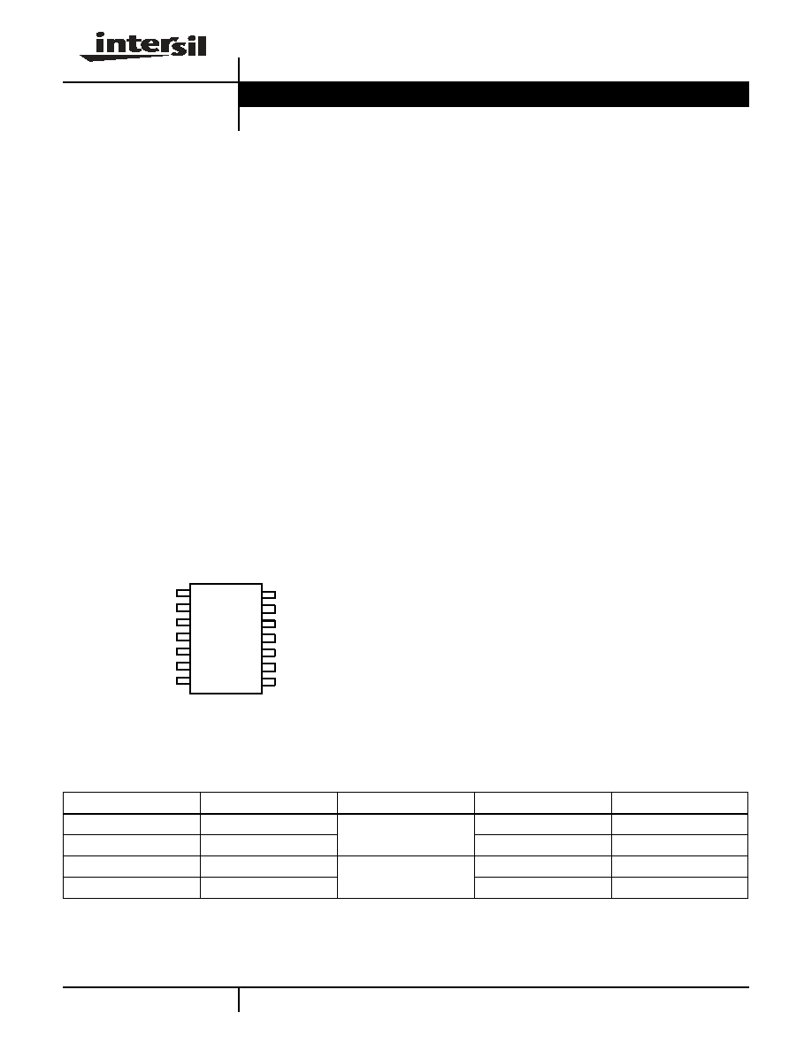
Pinout
X9460
(14 LD TSSOP)
TOP VIEW
Features
∑ Dual Audio Control ≠ Two 32 Taps Log Pots
∑ Zero Amplitude Wiper Switching
∑ 2-Wire Serial Interface
4 Slave Byte Addresses for Writes[A1,A0]
∑ Total Resistance: 33k
Each XDCP (Typical)
∑ Dual Voltage Operation
V+/V- = ±2.7 to ±5.5V
∑ Temp Range = -40∞C to +85∞C
∑ Package Options
14 L d TSSOP
∑ Zero Amplitude Wiper Switching
∑ Pb-Free Plus Anneal Available (RoHS Compliant)
Audio Performance
∑ 0 to - 62dB Volume Control
∑ -92dB Mute
- Power-Up to Mute Position
∑ SNR -96dB
∑ THD+N: -95dB @1kHz
∑ Crosstalk Rejection: -102dB @ 1kHz
∑ Channel-to-Channel Variation: ± 0.1dB
∑ 3dB-Cutoff: 100kHz
Applications
∑ Set Top Boxes
∑ Stereo Amplifiers
∑ DVD Players
∑ Portable Audio Products
V
CC
R
H-left
SDA
V
SS
1
2
3
4
5
6
7
8
14
13
12
11
10
9
V+
A1
R
H-right
R
L-right
R
W-right
SCL
A0
V-
R
L-left
R
W-left
X9460
Ordering Information
PART NUMBER
PART MARKING
V
CC
LIMITS (V)
TEMP RANGE (∞C)
PACKAGE
X9460KV14I*
X9460KV I
5V ± 10%
-40 to +85
14 Ld TSSOP
X9460KV14IZ* (Note)
X9460KV Z I
-40 to +85
14 Ld TSSOP (Pb-free)
X9460KV14I-2.7*
X9460KV G
2.7 to 5.5
-40 to +85
14 Ld TSSOP
X9460KV14IZ-2.7* (Note)
X9460KV Z G
-40 to +85
14 Ld TSSOP (Pb-free)
*Add "T1" suffix for tape and reel.
NOTE: Intersil Pb-free plus anneal products employ special Pb-free material sets; molding compounds/die attach materials and 100% matte tin plate
termination finish, which are RoHS compliant and compatible with both SnPb and Pb-free soldering operations. Intersil Pb-free products are MSL
classified at Pb-free peak reflow temperatures that meet or exceed the Pb-free requirements of IPC/JEDEC J STD-020.
Data Sheet
October 17, 2005
2
FN8203.2
October 17, 2005
Simplified Functional Diagram
Detailed Functional Diagram
R
H-Right
R
L-Right
BUS
R
H-Left
R
L-Left
R
W-Left
R
W-Right
INTERFACE
CONTROL &
REGISTER
POT
Left
POT
Right
V
SS
I
2
C
bus
V-
data
address
select
inc/dec
Power-on
Recall
mute
V
CC
62dB total
STEP SIZE
# OF
STEPS
-1dB
11
-2dB
10
-3dB
5
-4dB
4
Mute
1
V+
R
H-Right
R
L-Right
WIPER
COUNTER
REGISTER
(WCR)
INTERFACE
AND
CONTROL
CIRCUITRY
SCL
A0
R
H-Left
R
L-Left
D ATA
8
R
W-Left
R
W-Right
WIPER
COUNTER
REGISTER
(WCR)
SDA
A1
V-
V
SS
Power-on
Recall
mute
POT Right
POT Left
V
CC
V+
X9460
3
FN8203.2
October 17, 2005
Typical Application
Left Channel Control
Right Channel Control
Simultaneous Left and Right Channel
Control
Gain / Volume Control
Power-up in Mute
Audio
DAC
Audio
Amplifier
Left
Audio
Amplifier
Right
µController
EEPROM
X9460
2 XDCP
Serial Bus
Audio => R
HL,
R
HR
R
WL
, R
WR
=> Amplifier
Pin Assignments
PIN
(TSSOP)
SYMBOL
FUNCTION
1
SDA
Serial Data
2
SCL
Serial Clock
3
V
CC
System Supply Voltage
4
V+
Positive Analog Supply
5
V
SS
System Ground
6
A0
Device Address
7
A1
Device Address
8
R
W-left
Wiper terminal of the Left Potentiometer
9
R
L-left
Negative terminal of the Left Potentiometer
10
R
H-left
Positive terminal of the Left Potentiometer
11
R
W-right
Wiper terminal of the Right Potentiometer
12
R
L-right
Negative terminal of the Right Potentiometer
13
R
H-right
Positive terminal of the Right Potentiometer
14
V-
Negative Analog Supply
X9460
4
FN8203.2
October 17, 2005
Detailed Pin Description
Host Interface Pins
SERIAL CLOCK (SCL)
The SCL input clocks data into and out of the X9460.
SERIAL DATA (SDA)
SDA is a bidirectional pin used to transfer data into and out
of the device. It is an open drain output and may be wire-
ORed with any number of open drain or open collector
outputs. An open drain output requires the use of a pull-up
resistor. For selecting typical values, refer to the guidelines
for calculating typical values on the bus pull-up resistors
graph.
DEVICE ADDRESS (A
1
- A
0
)
The Address inputs are used to set the least significant 2 bits
of the 8-bit Slave Byte Address. A match in the slave
address serial data stream must be made with the Address
input in order to initiate communication with the X9460. Up to
4 X9460s may be connected to a single I
2
C serial bus and
written to (NOTE: you cannot read from more than one
device on the same 2-wire bus). If left floating, these pins are
internally pulled to ground.
Slave Byte (bits, MSB-LSB) = 0101 0 A
1
A
0
R/W
Potentiometer Pins
R
H-LEFT
, R
L-LEFT
, R
H-RIGHT
, R
L-RIGHT
The R
H
and R
L
inputs are equivalent to the terminal
connections on either end of a mechanical potentiometer.
R
W-LEFT
, R
W-RIGHT
The wiper outputs are equivalent to the wiper output of a
mechanical potentiometer.
Supply Pins
ANALOG SUPPLY V- AND V+
The positive power supply for the DCP analog control
section is connected to V+. The negative power supply for
the DCP analog control section is connected to V-.
DIGITAL SUPPLIES V
CC
, V
SS
The power supplies for the digital control sections.
Power-up and Down Recommendations
There are no restrictions on the power-up condition of V
CC
,
V+ and V- and the voltages applied to the potentiometer pins
provided that the V
CC
and V+ are more positive or equal to
the voltage at R
H
, R
L
, and R
W
, ie. V
CC
, V+ > R
H
, R
L
, R
W
. At
all times, the voltages on the potentiometer pins must be
less than V+ and more than V-.
The following V
CC
ramp rate spec is always in effect.
0.2 V/ms < V
CC
ramp < 50 V/ms
The V
SS
pin is always connected to the system common or
ground. V
H
, V
L
, V
W
are the voltages on the R
H
, R
L
, and R
W
potentiometer pins.
X9460 Principles of Operation
The X9460 is a highly integrated microcircuit incorporating
two resistor arrays with their associated registers, counters
and the serial interface logic providing direct communication
between the host and the DCP potentiometers. This section
provides detailed description as following:
- Resistor Array Description
- Serial Interface Description
- Command Set and Register Information Description
Resistor Array Description
The X9460 is comprised of two resistor arrays. Each array
contains 31 discrete resistive segments that are connected
in series. The physical ends of each array are equivalent to
the fixed terminals of a mechanical potentiometer (R
H
and
R
L
inputs). Tables 1 and 2 provide a description of the step
size and tap positions.
At both ends of each array and between each resistor
segment is a CMOS switch connected to the wiper (R
W
)
output. Within each individual array only one switch may be
turned on at a time. These switches are controlled by the
Wiper Counter Register (WCR). The five bits of the WCR are
decoded to select, and enable, one of thirty-two switches.
TABLE 1. TOTAL -62dB RANGE PLUS MUTE POSITION
STEP SIZE
# OF STEPS
-1dB
11 steps
- 2dB
10 steps
- 3dB
5 steps
- 4dB
4 steps
Mute
1 step
TABLE 2. WIPER TAP POSITION vs dB
TAP POSITION, n
dB
MIN/MAX dB
for n = 20 to 31
n - 31
-11/0
for n = 10 to 19
2n-51
-31/-13
for n = 5 to 9
3n-61
-46/-34
for n = 1 to 4
4n-66
-62/-50
n = 0
-92
-92
X9460
5
FN8203.2
October 17, 2005
Serial Interface Description
Serial Interface
The X9460 supports a bidirectional bus oriented protocol.
The protocol defines any device that sends data onto the
bus as a transmitter and the receiving device as the receiver.
The device controlling the transfer is a master and the
device being controlled is the slave. The master will always
initiate data transfers and provide the clock for both transmit
and receive operations. The X9460 is a slave device in all
applications.
Clock and Data Conventions
Data states on the SDA line can change only during SCL
LOW periods. SDA state changes during SCL HIGH are
reserved for indicating start and stop conditions.
Start Condition
All commands to the X9460 are preceded by the start
condition, which is a HIGH to LOW transition of SDA while
SCL is HIGH. The X9460 continuously monitors the SDA
and SCL lines for the start condition and will not respond to
any command until this condition is met.
Stop Condition
All communications must be terminated by a stop condition,
which is a LOW to HIGH transition of SDA while SCL is
HIGH.
Acknowledge
Acknowledge is a software convention used to provide a
positive handshake between the master and slave devices
on the bus to indicate the successful receipt of data. The
transmitting device, either the master or the slave, will
release the SDA bus after transmitting eight bits. The master
generates a ninth clock cycle and during this period the
receiver pulls the SDA line LOW to acknowledge that it
successfully received the eight bits of data.
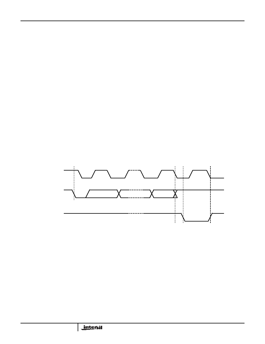
The X9460 will respond with an acknowledge: 1) after
recognition of a start condition and after an identification and
slave address byte, and 2) again after each successful
receipt of the instruction or databyte. See Figure 1.
Invalid Commands
For any invalid commands or unrecognizable addresses, the
X9460 will NOT acknowledge and return the X9460 to the
idle state.
SCL FROM
MASTER
DATA
OUTPUT
FROM
TRANSMITTER
1
8
9
DATA
OUTPUT
FROM
RECEIVER
ST AR T
ACKNOWLEDGE
FIGURE 1. ACKNOWLEDGE RESPONSE FROM RECEIVER
X9460

6
FN8203.2
October 17, 2005
Command Set and Register Description
Device Addressing
Following a start condition the master must output the Slave
Byte Address of the slave it is accessing. The most
significant four bits of the slave address are the device type
identifier (refer to Figure 2). For the X9460 this is fixed as
0101.
The next three bits of the Slave Byte Address are the device
address. The device address is defined by the A
1
- A
0
inputs.
The X9460 compares the serial data stream with the Slave
Byte Address; a successful compare is required for the
X9460 to respond with an acknowledge. The A
1
- A
0
inputs
can be actively driven by CMOS input signals or tied to V
CC
or V
SS
. The R/W bit sets the device for read or write
operations. Note that the X9460 supports reads and writes to
a single device on the 2-wire bus. If more than one X9460 is
used on the same 2-wire bus, those devices must have
unique device addresses and only writes are supported. You
may not read from multiple devices or contention will result
and the data is not valid.
Command Set
After a Slave Byte Address match, the next byte sent
contains the Command and register pointer information. The
four most significant bits are the Command. The next bit is a
"X" (don't care) set to zero.
The Z
D
bit enables and disables the Zero Amplitude Wiper
Switching circuit. When Z
D
=1, the wiper switches will turn on
when close-to-zero amplitude is detected across the
potentiometer pins. When Z
D
=0, this circuit is disabled. The
last two bits, LT (left POT enable) and RT (right POT
enable), select which of the two potentiometers is affected
by the instruction.
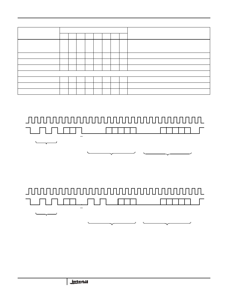
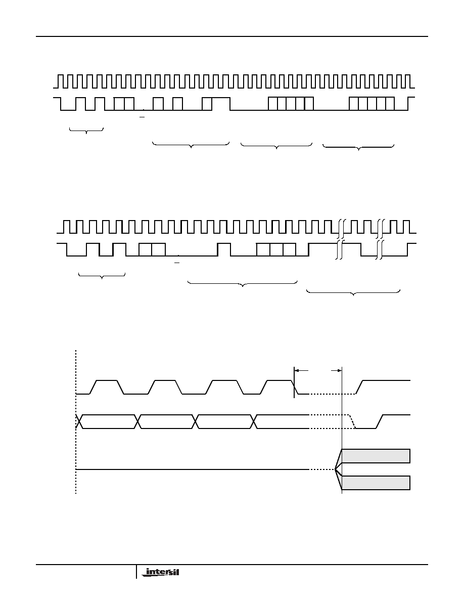
Several instructions require a three-byte sequence to
complete. These instructions transfer data between the host
and the X9460. These instructions are: Read Wiper Counter
Register, Write Wiper Counter Register. The sequence of
operations is shown in Figure 4 and 5. The four-byte
command is used for write command for both right and left
pots (Figure 6).
Special Commands
Increment/Decrement Instruction. The Increment/Decrement
command is different from the other commands. Once the
command is issued and the X9460 has responded with an
acknowledge, the master can clock the selected wiper up
and/or down. For each SCL clock pulse (t
HIGH
) while SDA is
HIGH, the selected wiper will move one resistor segment
towards the R
H
terminal. Similarly, for each SCL clock pulse
while SDA is LOW, the selected wiper will move one resistor
segment towards the R
L
terminal. A detailed illustration of
the sequence and timing for this operation are shown in
Figures 7 and 8 respectively.
Wiper Counter Register
The X9460 contains two Wiper Counter Registers. The
Wiper Counter Register output is decoded to select one of
thirty-two switches along its resistor array. The Write Wiper
Counter Register command directly sets the WCR to a
value. The Increment/Decrement instruction steps the
register value up or down one to multiple times.
The WCR is a volatile register (Table 3) and is reset to the
mute position (tap 0, "zero") at power-up.
TABLE 3. WIPER COUNTER REGISTERS, 5-bit - VOLATILE:
The X9460 contains one 5-bit Wiper Counter Register for
each DCP. (Two 5-bit registers in total.)
1
0
0
0
A1
A0
R/W
DEVICE TYPE
IDENTIFIER
DEVICE ADDRESS
1
FIGURE 2. SLAVE BYTE ADDRESS
I1
I2
I3
I0
0
Z
D
RT
LT
WIPER COUNTER
SELECT
INSTRUCTIONS
this bit not used, set to 0
FIGURE 3. COMMAND BYTE FORMAT
WCR4
WCR3
WCR2
WCR1
WCR0
(MSB)
(LSB)
X9460
7
FN8203.2
October 17, 2005
Notes: "1/0" = data is one or zero
TABLE 4. COMMAND SET
INSTRUCTION
INSTRUCTION SET
OPERATION
I
3
I
2
I
1
I
0
X
Z
D
RT
LT
Read Wiper
LSB of Slave Byte=1, no command required
Slave will return Left then Right Data( not to be used with more
than one device on the 2-wire bus)
Write Left Wiper Counter
1
0
1
0
0
1/0
0
1
Write new value to the Wiper Counter Register
Write Right Wiper Counter
1
0
1
0
0
1/0
1
0
Write new value to the Wiper Counter Register
Write Both Wiper Counters
1
0
1
0
0
1/0
1
1
Write new value to the Wiper Counter Register
Inc/Dec Left Wiper Counter
0
0
1
0
0
1/0
0
1
Enable Increment/decrement of the Control Latch
Inc/Dec Right Wiper Counter
0
0
1
0
0
1/0
1
0
Enable Increment/decrement of the Control Latch
Inc/Dec Both Wiper Counters
0
0
1
0
0
1/0
1
1
Enable Increment/decrement of the Control Latch
S
T
A
R
T
0
1
0
1
0
A1 A0 R/W A
C
K
0
0
0
SCL
SDA
S
T
O
P
A
C
K
0
0
0
LEFT POT
DATA BYTE
RIGHT POT
DATA BYTE
DEVICE TYPE
IDENTIFIER
1
0
0
0
0
0
0
A
C
K
W
C
R
4
W
C
R
3
W
C
R
2
W
C
R
1
W
C
R
0
W
C
R
4
W
C
R
3
W
C
R
2
W
C
R
1
W
C
R
0
FIGURE 4. THREE-BYTE COMMAND SEQUENCE (READ, SINGLE DEVICE ON THE 2-WIRE BUS ONLY)
S
T
A
R
T
0
1
0
1
0
A1 A0
R/W A
C
K
I3
I2
I1
I0
0
ZD
RT LT
A
C
K
SCL
SDA
S
T
O
P
A
C
K
0
0
0
INSTRUCTION BYTE
RIGHT or LEFT POT
DATA BYTE
DEVICE TYPE
IDENTIFIER
0
1
0
1
0
0
0
0
0
W
C
R
4
W
C
R
3
W
C
R
2
W
C
R
1
W
C
R
0
FIGURE 5. THREE-BYTE COMMAND SEQUENCE (WRITE)
X9460
8
FN8203.2
October 17, 2005
S
T
A
R
T
0 1
0
1 0
A1 A0 R/W A
C
K
I3 I2
I1 I0 0 ZD RT LT A
C
K
SCL
SDA
INSTRUCTION BYTE
DEVICE TYPE
IDENTIFIER
0 0
0
A
C
K
S
T
O
P
A
C
K
0 0 0
LEFT POT
DATA BYTE
RIGHT POT
DATA BYTE
0
1
0
1
0
0
1
1
0 0
0
0 0 0
W
C
R
4
W
C
R
3
W
C
R
2
W
C
R
1
W
C
R
0
W
C
R
4
W
C
R
3
W
C
R
2
W
C
R
1
W
C
R
0
FIGURE 6. FOUR-BYTE COMMAND SEQUENCE (WRITE)
S
T
A
R
T
0
1
0
1
0
A1
A0
R/W A
C
K
I3
I2
I1
I0
ZD
RT LT
A
C
K
SCL
SDA
S
T
O
P
I
N
C
1
I
N
C
2
I
N
C
n
D
E
C
1
D
E
C
n
0
DEVICE TYPE
IDENTIFIER
INSTRUCTION BYTE
INC and DEC ACTIVE
0
0
0
0
1
0
FIGURE 7. INCREMENT/DECREMENT COMMAND SEQUENCE (WRITE)
SCL
SD A
RW
INC/DEC
CMD
ISSUED
VOLTAGE OUT
tWRID
Wiper can move within 10µs after the falling edge of SCL
FIGURE 8. INCREMENT/DECREMENT TIMING LIMITS
X9460
9
FN8203.2
October 17, 2005
Instruction Formats
Read Wiper Counter Register (Single device on 2-wire bus only)
Write Wiper Counter Register
Write Both Wiper Counter Registers
Increment/Decrement Wiper Counter Register
Definitions:
1. "MACK"/"SACK": stands for the acknowledge sent by the master/slave.
2. "A1 ~ A0": stands for the device addresses sent by the master.
3. "I": stands for the increment operation, SDA held high during active SCL phase (high).
4. "D": stands for the decrement operation, SDA held low during active SCL phase (high).
S
T
A
R
T
device type
identifier
device
addresses
S
A
C
K
Left wiper position
(sent by slave on SDA)
M
A
C
K
Right wiper position
(sent by slave on SDA)
M
A
C
K
S
T
O
P
0 1 0 1 0 A
1
A
0
R /
W
= 1
0 0 0
L
D
4
L
D
3
L
D
2
L
D
1
L
D
0
0 0 0
R
D
4
R
D
3
R
D
2
R
D
1
R
D
0
S
T
A
R
T
device type
identifier
device
addresses
S
A
C
K
instruction
opcode
wiper
addresses S
A
C
K
Left or Right wiper
position
(sent by master on SDA)
S
A
C
K
S
T
O
P
0 1 0 1 0 A
1
A
0
R / W
= 0
1 0 1 0 0 Z
D
R
T
L
T
0 0 0 D
4
D
3
D
2
D
1
D
0
S
T
A
R
T
device type
identifier
device
addresses S
A
C
K
instruction
opcode
wiper
addresses S
A
C
K
Left wiper position
(sent by master on
SDA)
S
A
C
K
Right wiper position
(sent by master on
SDA)
S
A
C
K
S
T
O
P
0 1 0 1 0 A
1
A
0
R / W
= 0
1 0 1 0 0 Z
D 1 1
0 0 0
L
D
4
L
D
3
L
D
2
L
D
1
L
D
0
0 0 0
R
D
4
R
D
3
R
D
2
R
D
1
R
D
0
S
T
A
R
T
device type
identifier
device
addresses
S
A
C
K
instruction
opcode
wiper
addresses
S
A
C
K
increment/decrement
(sent by master on SDA)
S
T
O
P
0 1 0 1
0
A1 A0
R /
W
= 0
0 0 1 0 0 ZD RT LT
I/D I/D .
.
.
. I/D I/D
X9460
10
FN8203.2
October 17, 2005
Absolute Maximum Ratings
Recommended Operating Conditions
Temperature under Bias. . . . . . . . . . . . . . . . . . . . . .-65
∞C to +135∞C
Storage Temperature . . . . . . . . . . . . . . . . . . . . . . . .-65
∞C to +150∞C
Voltage on SDA, SCL or any Address Input
with Respect to V
SS
. . . . . . . . . . . . . . . . . . . . . . . . . . . . -1V to +6V
Voltage on V+ (referenced to V
SS
). . . . . . . . . . . . . . . . . . . . . . . .+6V
Voltage on V- (referenced to V
SS
) . . . . . . . . . . . . . . . . . . . . . . . . -6V
(V+) - (V-) . . . . . . . . . . . . . . . . . . . . . . . . . . . . . . . . . . . . . . . . . . .12V
Any R
H
. . . . . . . . . . . . . . . . . . . . . . . . . . . . . . . . . . . . . . . . . . . . . .V+
Any R
L
. . . . . . . . . . . . . . . . . . . . . . . . . . . . . . . . . . . . . . . . . . . . . . V-
Lead Temperature (Soldering, 10s) . . . . . . . . . . . . . . . . . . . . . 300
∞C
I
W
max (10s) . . . . . . . . . . . . . . . . . . . . . . . . . . . . . . . . . . . . . . ±3mA
Temperature Range (Industrial) . . . . . . . . . . . . . . . . . . -40∞C to 85∞C
X9460V14-2.7
Supply Voltage (V
CC
) . . . . . . . . . . . . . . . . . . . . . . . . . 2.7V to 5.5V
V- Limits . . . . . . . . . . . . . . . . . . . . . . . . . . . . . . . . . . -5.5V to -2.7V
V+ Limits . . . . . . . . . . . . . . . . . . . . . . . . . . . . . . . . +2.7V to +5.5V
CAUTION: Stresses above those listed under "Absolute Maximum Ratings" may cause permanent damage to the device. This is a stress rating only; functional operation
of the device (at these or any other conditions above those listed in the operational sections of this specification) is not implied. Exposure to absolute maximum rating
conditions for extended periods may affect device reliability.
Analog Specifications
Over the recommended operating conditions unless otherwise specified (Note 1)
SYMBOL
PARAMETER
TEST CONDITIONS
MIN
TYP
MAX
UNIT
DYNAMIC PERFORMANCE (Notes 2, 3)
Control Range
-62
0
dB
Mute Mode
@1V rms
-92
dB
SNR
Signal Noise Ratios (Unweighted)
@1V rms @ 1kHz, Tap = -6dB
-96
dB
THD + N
Total Harmonic Distortion + Noise
@1V rms @ 1kHz, Tap = -6dB
-95
dB
XTalk
DCP Isolation
@1kHz, tap = -6dB
-102
dB
Digital Feedthrough
(Peak Component)
tap = -6dB
-105
dB
-3db Cutoff Frequency
100
kHz
DC ACCURACY
Step Size
Steps of -1, -2, -3, -4 dB
-1
-4
dB
Step Size Error
For -1dB steps
-0.2
+0.2
dB
Step Size Error
For -2dB steps
-0.4
+0.4
dB
Step Size Error
For -3dB steps
-0.6
+0.6
dB
Step Size Error
For -4dB steps
-0.8
+0.8
dB
DCP to DCP Matching
-0.1
0.1
dB
NOTES:
1. V
CC
= | V- |
V
CC
Ramp up timing 0.2V/ms < Vcc Ramp Rate < 50V/ms
2. This parameter is guaranteed by design and characterization
3. T
A
= 25
o
C, V
CC
= 5.0V; 2 Hz to 20kHz Measurement Bandwidth with 80kHz filter, input signal 1Vrms, 1kHz Sine Wave.
Analog Specifications
Over the recommended operating conditions unless otherwise specified (Note 1)
ANALOG INPUTS
SYMBOL
PARAMETER
TEST CONDITIONS
MIN
TYP
MAX
UNIT
V
TERM
Voltage on R
L
, R
W
, and R
H
pins
V-
V+
V
R
TOTAL
End to End Resistance
Typical 33k
-20
+20
%
Cin (Note 4) Input Capacitance R
L
, R
H
, R
W
T
A
= 25
o
C
25
pF
I
W
(NOte 2) Wiper Current
-3
+3
mA
R
W
Wiper Resistance
Wiper Current = ±3mA
100
200
V-
Voltage on V- pin
-5.5
-2.7
V
X9460
11
FN8203.2
October 17, 2005
V+
Voltage on V+ pin
+2.7
+5.5
V
Noise
20Hz to 20kHz, Grounded Input @ -6dB tap
2
µVrms
TC
R
(Note 2) Temperature Coefficient of resistance
-300
PPM/∞C
Analog Specifications
Over the recommended operating conditions unless otherwise specified (Note 1) (Continued)
ANALOG INPUTS
SYMBOL
PARAMETER
TEST CONDITIONS
MIN
TYP
MAX
UNIT
DC Electrical Specifications
Over the recommended operating conditions unless otherwise specified. (Note 1)
SYMBOL
PARAMETER
TEST CONDITIONS
LIMITS
MIN
TYP
MAX
UNITS
I
CC1
V
CC
Supply Current (Move Wiper,
Write, Read)
f
SCL
= 400kHz, SDA = Open,
Other Inputs = V
SS
200
300
µA
I
SB
V
CC
Current (Standby)
SCL = SDA = V
CC
, Addr. = V
SS
3
µA
I
LI
Input Leakage Current
V
IN
= V
SS
to V
CC
1
10
µA
Iai
Analog Input Leakage
V
IN
= V- to V+ with all other
analog inputs floating
0.1
µA
I
LO
Output Leakage Current
V
OUT
= V
SS
to V
CC
10
µA
V
IH
Input HIGH Voltage
V
CC
x 0.7
V
CC
+ 0.5
V
V
IL
Input LOW Voltage
-0.5
V
CC
x 0.1
V
V
OL
Output LOW Voltage
I
OL
= 3mA
0.4
V
Capacitance
SYMBOL
TEST
TEST CONDITIONS
MAX
UNITS
C
I/O
(Note 4)
Input/Output Capacitance (SDA)
V
I/O
= 0V
8
pF
C
IN
(NOte 4)
Input Capacitance (A0, A1, A2 and SCL)
V
IN
= 0V
6
pF
NOTE:
4. This parameter is not 100% tested.
X9460
12
FN8203.2
October 17, 2005
Equivalent A.C. Load Circuit
A.C. Test Conditions
Input Pulse Levels
V
CC
x 0.1 to V
CC
x 0.9
Input Rise and Fall Times
10ns
Input and Output Timing Level
V
CC
x 0.5
5V
1533
100pF
SDA OUTPUT
AC TIMING
Over recommended operating conditions
SYMBOL
PARAMETER
MIN
MAX
UNITS
f
SCL
Clock Frequency
400
kHz
t
CYC
Clock Cycle Time
2500
ns
t
HIGH
Clock High Time
600
ns
t
LOW
Clock Low Time
1300
ns
t
SU:STA
Start Setup Time
600
ns
t
HD:STA
Start Hold Time
600
ns
t
SU:STO
Stop Setup Time
600
ns
t
SU:DAT
SDA Data Input Setup Time
500
ns
t
HD:DAT
SDA Data Input Hold Time
50
ns
t
R
(Note 2)
SCL and SDA Rise Time
300
ns
t
F
(Note 2)
SCL and SDA Fall Time
300
ns
t
AA
(Note 2)
SCL Low to SDA Data Output Valid Time
900
ns
t
DH
(Note 2) SDA Data Output Hold Time
50
ns
T
I
(Note 2)
Noise Suppression Time Constant at SCL and SDA inputs
50
ns
t
BUF
(Note 2) Bus Free Time (Prior to Any Transmission)
1300
ns
t
SU:WPA
A0, A1 (Note 2)
0
ns
t
HD:WPA
A0, A1 (Note 2)
0
ns
DC Timing
(Note 2)
SYMBOL
PARAMETER
MIN
MAX
UNITS
t
WRPO
Wiper Response Time After The Third (Last) Power Supply Is Stable
10
µs
t
WRL
Wiper Response Time After Instruction Issued (All Load Instructions)
10
µs
t
WRID
Wiper Response Time From An Active SCL Edge (Increment/Decrement Instruction)
10
µs
X9460

13
FN8203.2
October 17, 2005
Timing Diagrams
t
SU:STA
t
HD:STA
t
SU:STO
SCL
SDA
t
R
(START)
(STOP)
t
F
t
R
t
F
FIGURE 9. START AND STOP TIMING
SCL
SDA
t
HIGH
t
LOW
t
CYC
t
HD:DAT
t
SU:DAT
t
BUF
FIGURE 10. INPUT TIMING
SCL
SDA
t
DH
t
AA
FIGURE 11. OUTPUT TIMING
SCL
SDA
VWx
(STOP)
LSB
t
WRL
FIGURE 12. DCP TIMING (FOR ALL LOAD INSTRUCTIONS)
X9460
14
FN8203.2
October 17, 2005
Typical Performance Characteristics
(V
cc
, V+ = 5.0V, V- = -5.0V, T
A
= + 25 ∞C, unless otherwise noted)
FFT Spectrum
-1 8 0
+0
-1 7 0
-1 6 0
-1 5 0
-1 4 0
-1 3 0
-1 2 0
-1 1 0
-1 0 0
-9 0
-8 0
-7 0
-6 0
-5 0
-4 0
-3 0
-2 0
-1 0
d
B
V
H z
(with 1kHz 1Vrms input, tap = -6dB)
20
20k
50
100
200
500
1k
2k
5k
10k
FIGURE 13. SINGLE TONE FREQUENCY RESPONSE
(with 80kHz low-pass filter, tap = -6dB)
THD+N vs Frequency
- 1 2 0
- 6 0
- 1 1 5
- 1 1 0
- 1 0 5
- 1 0 0
- 9 5
- 9 0
- 8 5
- 8 0
- 7 5
- 7 0
- 6 5
d
B
20
20k
50
100
200
500
1k
2k
5k
10k
Hz
FIGURE 14. THD + N
X9460

15
FN8203.2
October 17, 2005
Typical Performance Characteristics
(V
cc
, V+ = 5.0V, V- = -5.0V, T
A
= + 25 ∞C, unless otherwise noted)
Mut e Mod e
-140
+0
-130
-120
-110
-100
-90
-80
-70
-60
-50
-40
-30
-20
-10
d
B
V
20
20k
50
100
200
500
1k
2k
5k
10k
Hz
FIGURE 15. MUTE
X9460
16
All Intersil U.S. products are manufactured, assembled and tested utilizing ISO9000 quality systems.
Intersil Corporation's quality certifications can be viewed at www.intersil.com/design/quality
Intersil products are sold by description only. Intersil Corporation reserves the right to make changes in circuit design, software and/or specifications at any time without
notice. Accordingly, the reader is cautioned to verify that data sheets are current before placing orders. Information furnished by Intersil is believed to be accurate and
reliable. However, no responsibility is assumed by Intersil or its subsidiaries for its use; nor for any infringements of patents or other rights of third parties which may result
from its use. No license is granted by implication or otherwise under any patent or patent rights of Intersil or its subsidiaries.
For information regarding Intersil Corporation and its products, see www.intersil.com
FN8203.2
October 17, 2005
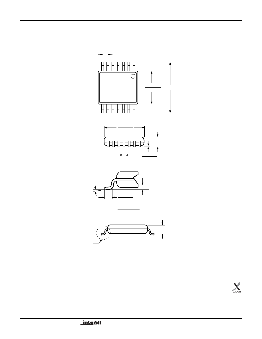
Packaging Information
NOTE: ALL DIMENSIONS IN INCHES (IN PARENTHESES IN MILLIMETERS)
14-Lead Plastic, TSSOP, Package Type V
See Detail "A"
.031 (.80)
.041 (1.05)
.169 (4.3)
.177 (4.5) .252 (6.4) BSC
.025 (.65) BSC
.193 (4.9)
.200 (5.1)
.002 (.05)
.006 (.15)
.047 (1.20)
.0075 (.19)
.0118 (.30)
0∞ - 8∞
.010 (.25)
.019 (.50)
.029 (.75)
Gage Plane
Seating Plane
Detail A (20X)
X9460