 | –≠–ª–µ–∫—Ç—Ä–æ–Ω–Ω—ã–π –∫–æ–º–ø–æ–Ω–µ–Ω—Ç: X9523 | –°–∫–∞—á–∞—Ç—å:  PDF PDF  ZIP ZIP |
1
Æ
FN8209.0
CAUTION: These devices are sensitive to electrostatic discharge; follow proper IC Handling Procedures.
1-888-INTERSIL or 1-888-352-6832 | Intersil (and design) is a registered trademark of Intersil Americas Inc.
©2000 Intersil Inc., Patents Pending. Copyright Intersil Americas Inc. 2005. All Rights Reserved
All other trademarks mentioned are the property of their respective owners.
PRELIMINARY
X9523
Laser Diode Control for Fiber Optic Modules
Dual DCP, POR, Dual Voltage Monitors
FEATURES
∑ Two Digitally Controlled Potentiometers (DCPs)
--100 Tap - 10k
--256 Tap - 100k
--Nonvolatile
--Write Protect Function
∑ 2-Wire industry standard Serial Interface
∑ Power-On Reset (POR) Circuitry
--Programmable Threshold Voltage
--Software Selectable reset timeout
--Manual Reset
∑ Two Supplementary Voltage Monitors
--Programmable Threshold Voltages
∑ Single Supply Operation
--2.7V to 5.5V
∑ Hot Pluggable
∑ 20 Pin packages
--XBGA
TM
--TSSOP
DESCRIPTION
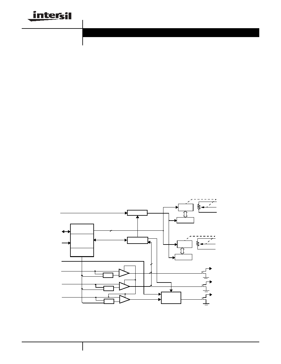
The X9523 combines two Digitally Controlled Potenti-
ometers (DCPs), V1 / Vcc Power-on Reset (POR) cir-
cuitry, qnd two programmable voltage monitor inputs
with software and hardware indicators. All functions of
the X9523 are accessed by an industry standard 2-Wire
serial interface.
The DCPs of the X9523 may be utilized to control the
bias and modulation currents of the laser diode in a Fiber
Optic module. The programmable POR circuit may be
used to ensure that V1 / Vcc is stable before power is
applied to the laser diode / module. The programmable
voltage monitors may be used for monitoring various
module alarm levels.
The features of the X9523 are ideally suited to simpli-
fying the design of fiber optic modules . The integra-
tion of these functions into one package significantly
reduces board area, cost and increases reliability of
laser diode modules.
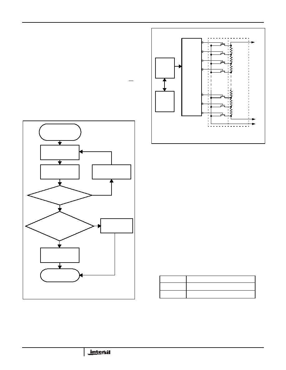
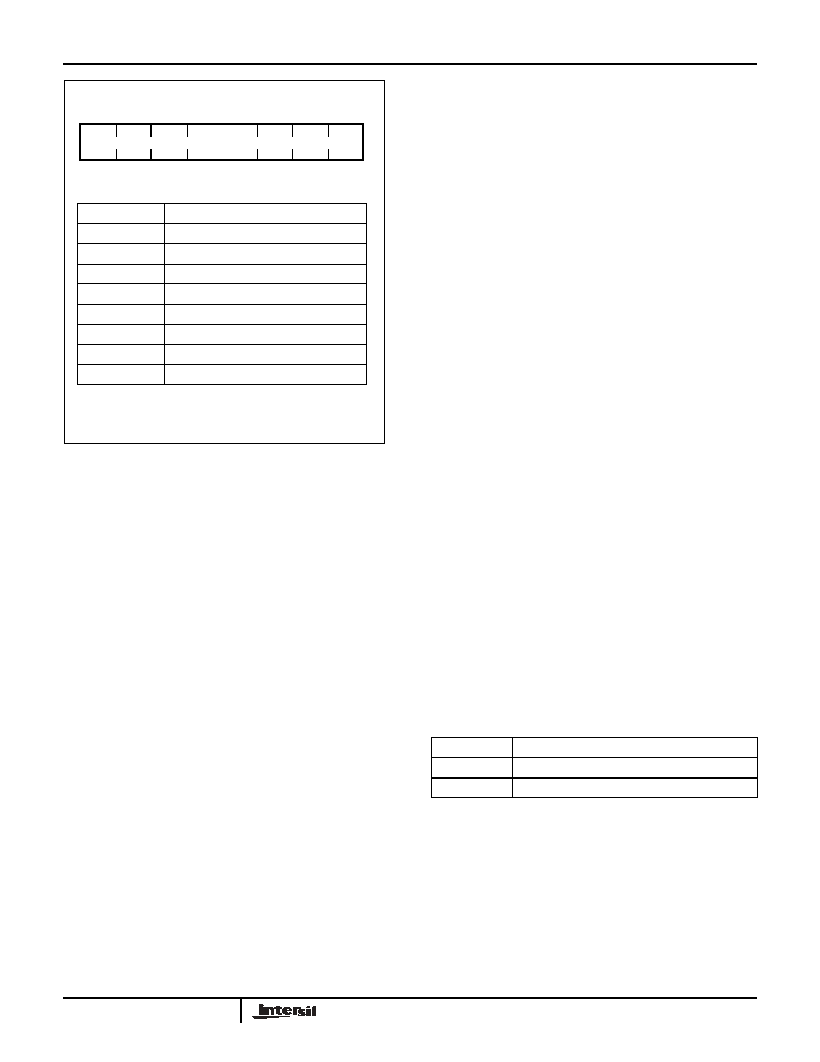
BLOCK DIAGRAM
DATA
REGISTER
COMMAND
DECODE &
CONTROL
LOGIC
SDA
SCL
POWER-ON /
LOW VOLTAGE
CONSTAT
REGISTER
PROTECT LOGIC
THRESHOLD
RESET LOGIC
GENERATION
RESET
V2
VTRIP
V1 / Vcc
VTRIP
V3
+
-
2
3
1
V1RO
R
H2
R
W2
R
L2
MR
8
WIPER
REGISTER
R
H1
R
W1
R
L1
COUNTER
V2RO
WP
V3RO
7 - BIT
NONVOLATILE
MEMORY
NONVOLATILE
MEMORY
WIPER
REGISTER
COUNTER
8 - BIT
2
VTRIP
+
-
+
-
Data Sheet
March 10, 2005
2
FN8209.0
March 10, 2005
DETAILED DEVICE DESCRIPTION
The X9523 combines two Intersil Digitally Controlled
Potentiometer (DCP) devices, V1/Vcc power-on reset
control, V1/Vcc low voltage reset control, and two sup-
plementary voltage monitors in one package. These
functions are suited to the control, support, and monitor-
ing of various system parameters in fiber optic modules.
The combination of the X9523 fucntionality lowers sys-
tem cost, increases reliability, and reduces board space
requirements using Intersil's unique XBGATM packaging.
Two high resolution DCPs allow for the "set-and-forget"
adjustment of Laser Driver IC parameters such as Laser
Diode Bias and Modulation Currents.
Applying voltage to V
CC
activates the Power-on Reset
circuit which allows the V1RO output to go HIGH, until
the supply the supply voltage stabilizes for a period of
time (selectable via software). The V1RO output then
goes LOW. The Low Voltage Reset circuitry allows the
V1RO output to go HIGH when V
CC
falls below the mini-
mum V
CC
trip point. V1RO remains HIGH until V
CC
returns to proper operating level. A Manual Reset (MR)
input allows the user to externally trigger the V1RO out-
put (HIGH).
Two supplementary Voltage Monitor circuits continuously
compare their inputs to individual trip voltages. If an input
voltage exceeds it's associated trip level, a hardware out-
put (V3RO, V2RO) are allowed to go HIGH. If the input
voltage becomes lower than it's associated trip level, the
corresponding output is driven LOW. A corresponding
binary representation of the two monitor circuit outputs
(V2RO and V3RO) are also stored in latched, volatile
(CONSTAT) register bits. The status of these two moni-
tor outputs can be read out via the 2-wire serial port.
Intersil's unique circuits allow for all internal trip volt-
ages to be individually programmed with high accu-
racy. This gives the designer great flexibility in
changing system parameters, either at the time of
manufacture, or in the field.
The device features a 2-Wire interface and software
protocol allowing operation on an I
2
CTM compatible
serial bus.
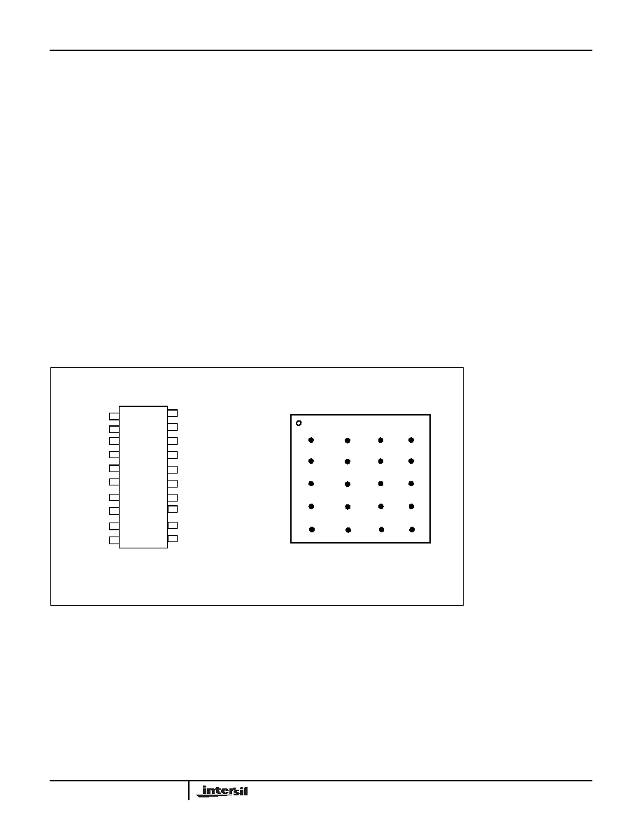
PIN CONFIGURATION
V2
R
L2
NC
3
4
V1 / Vcc
SCL
NC
NC
R
W1
R
H1
7
8
V3
V
SS
10
R
L1
R
H2
1
18
19
17
20
14
15
13
16
12
11
MR
6
R
W2
2
SDA
9
V3RO
5
WP
V1RO
V2RO
NOT TO SCALE
XBGA
20 Pin TSSOP
2
3
4
A
B
C
D
E
Top View ≠ Bumps Down
1
R
L2
R
W2
R
H2
V2
WP
V3RO
SCL
NC
SDA
R
L1
V2RO
V1 / Vcc
V3
V1RO
NC
NC
R
H1
MR
V
SS
R
W1
X9523
3
FN8209.0
March 10, 2005
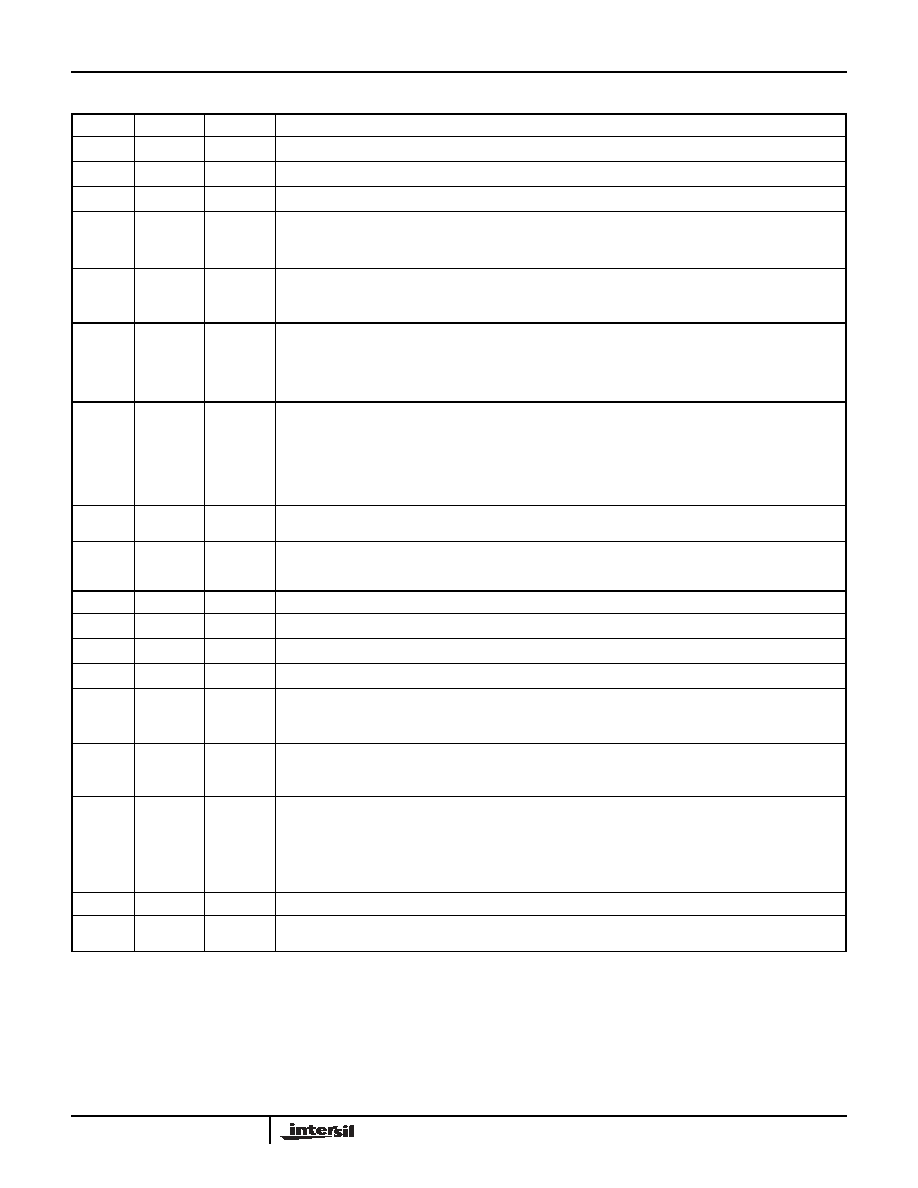
PIN ASSIGNMENT
Pin
XBGA
Name
Function
1
B3
R
H2
Connection to end of resistor array for (the 256 Tap) DCP 2.
2
A3
R
w2
Connection to terminal equivalent to the "Wiper" of a mechanical potentiometer for DCP 2.
3
A4
R
L2
Connection to other end of resistor array for (the 256 Tap) DCP 2.
4
B4
V3
V3 Voltage Monitor Input. V3 is the input to a non-inverting voltage comparator circuit. When
the V3 input is higher than the
V
TRIP3
threshold voltage, V3RO makes a transition to a HIGH
level. Connect V3 to V
SS
when not used.
5
C3
V3RO
V3 RESET Output. This open drain output makes a transition to a HIGH level when V3 is
greater than
V
TRIP3 and goes LOW when V3 is less than VTRIP3. There is no delay circuitry
on this pin. The V3RO pin requires the use of an external "pull-up" resistor.
6
D3
MR
Manual Reset. MR is a TTL level compatible input. Pulling the MR pin active (HIGH) initiates
a reset cycle to the V1RO pin (V1/Vcc RESET Output pin). V1RO will remain HIGH for time
t
purst
after MR has returned to it's normally LOW state. The reset time can be selected using
bits POR1 and POR0 in the CONSTAT Register. The MR pin requires the use of an external
"pull-down" resistor.
7
C4
WP
Write Protect Control Pin. WP pin is a TTL level compatible input. When held HIGH, Write Pro-
tection is enabled. In the enabled state, this pin prevents all nonvolatile "write" operations. Al-
so, when the Write Protection is enabled, and the device DCP Write Lock feature is active (i.e.
the DCP Write Lock bit is "1"), then no "write" (volatile or nonvolatile) operations can be per-
formedon the wiper position of any of the integrated Digitally Controlled Potentiometers
(DCPs). The WP pin uses an internal "pull-down" resistor, thus if left floating the write protec-
tion feature is disabled.
8
D4
SCL
Serial Clock. This is a TTL level compatible input pin used to control the serial bus timing for
data input and output.
9
E4
SDA
Serial Data. SDA is a bidirectional TTL level compatible pin used to transfer data into and
out of the device. The SDA pin input buffer is always active (not gated). This pin requires an
external pull up resistor.
10
E1
Vss
Ground.
11
E3
R
L1
Connection to other end of resistor for (the 100 Tap) DCP 1.
12
E2
R
w1
Connection to terminal equivalent to the "Wiper" of a mechanical potentiometer for DCP 1.
13
D1
R
H1
Connection to end of resistor array for (the 100 Tap) DCP 1.
17
B1
V2
V2 Voltage Monitor Input. V2 is the input to a non-inverting voltage comparator circuit. When
the V2 input is greater than the
V
TRIP2
threshold voltage, V2RO makes a transition to a HIGH
level. Connect V2 to V
SS
when not used.
18
A1
V2RO
V2 RESET Output. This open drain output makes a transition to a HIGH level when V2 is great-
er than
V
TRIP2
, and goes LOW when V2 is less than
V
TRIP2
. There is no power-up reset delay
circuitry on this pin. The V2RO pin requires the use of an external "pull-up" resistor.
19
B2
V1RO
V1 / Vcc RESET Output. This is an active HIGH, open drain output which becomes active
whenever V1 / Vcc falls below
V
TRIP1
. V1RO becomes active on power-up and remains ac-
tive for a time t
purst
after the power supply stabilizes (t
purst
can be changed by varying the
POR0 and POR1 bits of the internal control register). The V1RO pin requires the use of an
external "pull-up" resistor. The V1RO pin can be forced active (HIGH) using the manual reset
(MR) input pin.
20
A2
V1 / Vcc
Supply Voltage.
14, 15,
16,
C1, C2,
D2
NC
No Connect.
X9523

4
FN8209.0
March 10, 2005
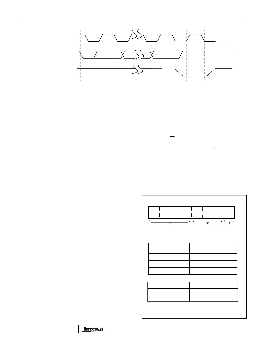
PRINCIPLES OF OPERATION
SERIAL INTERFACE
Serial Interface Conventions
The device supports a bidirectional bus oriented protocol.
The protocol defines any device that sends data onto the
bus as a transmitter, and the receiving device as the
receiver. The device controlling the transfer is called the
master and the device being controlled is called the
slave. The master always initiates data transfers, and
provides the clock for both transmit and receive opera-
tions. Therefore, the X9523 operates as a slave in all
applications.
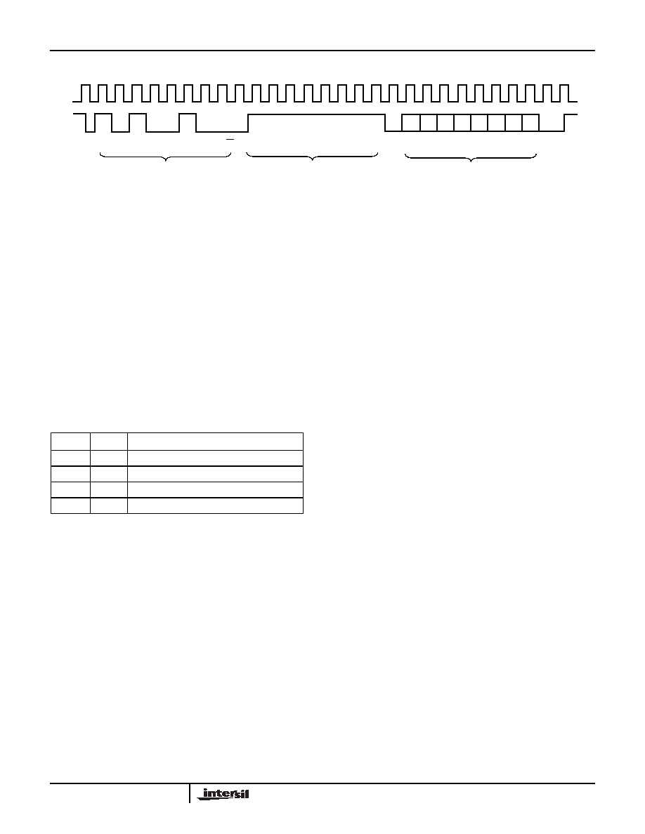
Serial Clock and Data
Data states on the SDA line can change only while SCL
is LOW. SDA state changes while SCL is HIGH are
reserved for indicating START and STOP conditions.
See Figure 1.On power-up of the X9523, the SDA pin is
in the input mode.
Serial Start Condition
All commands are preceded by the START condition,
which is a HIGH to LOW transition of SDA while SCL is
HIGH. The device continuously monitors the SDA and
SCL lines for the START condition and does not respond
to any command until this condition has been met. See
Figure 2.
Serial Stop Condition
All communications must be terminated by a STOP
condition, which is a LOW to HIGH transition of SDA
while SCL is HIGH. The STOP condition is also used to
place the device into the Standby power mode after a
read sequence. A STOP condition can only be issued
after the transmitting device has released the bus. See
Figure 2.
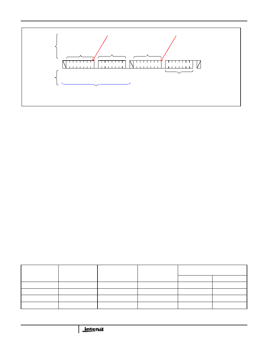
Serial Acknowledge
An ACKNOWLEDGE (ACK) is a software convention
used to indicate a successful data transfer. The trans-
mitting device, either master or slave, will release the
bus after transmitting eight bits. During the ninth clock
cycle, the receiver will pull the SDA line LOW to
ACKNOWLEDGE that it received the eight bits of data.
Refer to Figure 3.
The device will respond with an ACKNOWLEDGE after
recognition of a START condition if the correct Device
Identifier bits are contained in the Slave Address Byte. If
a write operation is selected, the device will respond with
an ACKNOWLEDGE after the receipt of each subse-
quent eight bit word.
In the read mode, the device will transmit eight bits of
data, release the SDA line, then monitor the line for an
ACKNOWLEDGE. If an ACKNOWLEDGE is detected
and no STOP condition is generated by the master, the
device will continue to transmit data. The device will ter-
SCL
SDA
Data Stable
Data Change
Data Stable
Figure 1.
Valid Data Changes on the SDA Bus
SCL
SDA
Start
Stop
Figure 2.
Valid Start and Stop Conditions
X9523
5
FN8209.0
March 10, 2005
minate further data transmissions if an ACKNOWLEDGE
is not detected. The master must then issue a STOP
condition to place the device into a known state.
DEVICE INTERNAL ADDRESSING
Addressing Protocol Overview
The user addressable internal components of the X9523
can be split up into two main parts:
--Two Digitally Controlled Potentiometers (DCPs)
--Control and Status (CONSTAT) Register
Depending upon the operation to be performed on
each of these individual parts, a 1, 2 or 3 Byte proto-
col is used. All operations however must begin with
the Slave Address Byte being issued on the SDA pin.
The Slave address selects the part of the X9523 to
be addressed, and specifies if a Read or Write opera-
tion is to be performed.
It should be noted that in order to perform a write opera-
tion to a DCP, the Write Enable Latch (WEL) bit must first
be set (See "WEL: Write Enable Latch (Volatile)" on
page 10.).
Slave Address Byte
Following a START condition, the master must output a
Slave Address Byte (Refer to Figure 4.). This byte con-
sists of three parts:
--The Device Type Identifier which consists of the most
significant four bits of the Slave Address (SA7 - SA4).
The Device Type Identifier must always be set to 1010
in order to select the X9523.
--The next three bits (SA3 - SA1) are the Internal Device
Address bits. Setting these bits to 111 internally
selects the DCP structures in the X9523. The CON-
STAT Register may be selected using the Internal
Device Address 010.
--The Least Significant Bit of the Slave Address (SA0)
Byte is the R/W bit. This bit defines the operation to be
performed on the device being addressed (as defined
in the bits SA3 - SA1). When the R/W bit is "1", then a
READ operation is selected. A "0" selects a WRITE
operation (Refer to Figure 4.)
Nonvolatile Write Acknowledge Polling
After a nonvolatile write command sequence (for either
the Non Volatile Memory of a DCP (NVM), or the CON-
STAT Register) has been correctly issued (including the
SCL
from
Master
Data Output
from
Transmitter
Data Output
from
Receiver
8
1
9
Start
Acknowledge
Figure 3.
Acknowledge Response From Receiver
SCL
from
Master
SA6
SA7
SA5
SA3 SA2
SA1
SA0
DEVICE TYPE
IDENTIFIER
READ /
SA4
Internal Address
(SA3 - SA1)
Internally Addressed
Device
010
CONSTAT Register
111
DCP
All Others
RESERVED
Bit SA0
Operation
0
WRITE
1
READ
R/W
Figure 4.
Slave Address Format
1 0 1 0
WRITE
ADDRESS
INTERNAL
DEVICE
X9523
6
FN8209.0
March 10, 2005
final STOP condition), the X9523 initiates an internal high
voltage write cycle. This cycle typically requires 5 ms.
During this time, no further Read or Write commands can
be issued to the device. Write Acknowledge Polling is
used to determine when this high voltage write cycle has
been completed.
To perform acknowledge polling, the master issues a
START condition followed by a Slave Address Byte. The
Slave Address issued must contain a valid Internal
Device Address. The LSB of the Slave Address (R/W)
can be set to either 1 or 0 in this case. If the device is still
busy with the high voltage cycle then no
ACKNOWLEDGE will be returned. If the device has
completed the write operation, an ACKNOWLEDGE will
be returned and the host can then proceed with a read or
write operation. (Refer to Figure 5.).
DIGITALLY CONTROLLED POTENTIOMETERS
DCP Functionality
The X9523 includes two independent resistor arrays.
These arrays respectively contain 99 and 255 discrete
resistive segments that are connected in series. The
physical ends of each array are equivalent to the fixed
terminals of a mechanical potentiometer (R
Hx
and R
Lx
inputs - where x = 1,2).
At both ends of each array and between each resistor
segment there is a CMOS switch connected to the wiper
(R
w
x
) output. Within each individual array, only one
switch may be turned on at any one time. These
switches are controlled by the Wiper Counter Register
(WCR) (See Figure 6). The WCR is a volatile register.
On power-up of the X9523, wiper position data is auto-
matically loaded into the WCR from its associated Non
Volatile Memory (NVM) Register. The Table below
shows the Initial Values of the DCP WCR's before the
contents of the NVM is loaded into the WCR.
ACK
returned?
Issue Slave Address
Byte (Read or Write)
Byte load completed
by issuing STOP.
Enter ACK Polling
Issue STOP
Issue START
NO
YES
High Voltage Cycle
complete. Continue
command sequence?
Issue STOP
NO
Continue normal
Read or Write
command sequence
PROCEED
YES
Figure 5.
Acknowledge Polling Sequence
DECODER
RESISTOR
ARRAY
R
Hx
FET
SWITCHES
R
Lx
R
Wx
0
1
2
N
WIPER
REGISTER
COUNTER
NON
MEMORY
VOLATILE
(WCR)
(NVM)
"WIPER"
Figure 6.
DCP Internal Structure
DCP
Initial Values Before Recall
R
1
/ 100 TAP
V
L
/ TAP = 0
R
2
/ 256 TAP
V
H
/ TAP = 255
X9523
7
FN8209.0
March 10, 2005
The data in the WCR is then decoded to select and
enable one of the respective FET switches. A "make
before break" sequence is used internally for the FET
switches when the wiper is moved from one tap position
to another.
Hot Pluggability
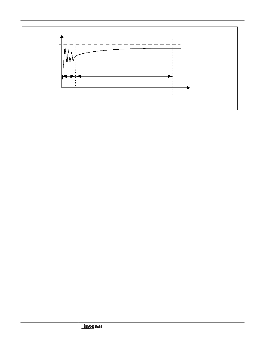
Figure 7 shows a typical waveform that the X9523 might
experience in a Hot Pluggable situation. On power-up,
V1 / Vcc applied to the X9523 may exhibit some amount
of ringing, before it settles to the required value.
The device is designed such that the wiper terminal
(R
Wx
) is recalled to the correct position (as per the last
stored in the DCP NVM), when the voltage applied to
V1/Vcc exceeds V
TRIP1
for a time exceeding t
purst
(the
Power-on Reset time, set in the CONSTAT Register -
See "CONTROL AND STATUS REGISTER" on
page 10.).
Therefore, if
t
trans
is defined as the time taken for V1 /
Vcc to settle above V
TRIP1
(Figure 7): then the desired
wiper terminal position is recalled by (a maximum) time:
t
trans
+
t
purst
. It should be noted that
t
trans
is determined
by system hot plug conditions.
DCP Operations
In total there are three operations that can be performed
on any internal DCP structure:
--DCP Nonvolatile Write
--DCP Volatile Write
--DCP Read
A nonvolatile write to a DCP will change the "wiper
position" by simultaneously writing new data to the
associated WCR and NVM. Therefore, the new "wiper
position" setting is recalled into the WCR after V1/Vcc of
the X9523 is powered down and then powered back up.
A volatile write operation to a DCP however, changes the
"wiper position" by writing new data to the associated
WCR only. The contents of the associated NVM register
remains unchanged. Therefore, when V1/Vcc to the
device is powered down then back up, the "wiper
position" reverts to that last position written to the DCP
using a nonvolatile write operation.
Both volatile and nonvolatile write operations are
executed using a three byte command sequence: (DCP)
Slave Address Byte, Instruction Byte, followed by a Data
Byte (See Figure 9)
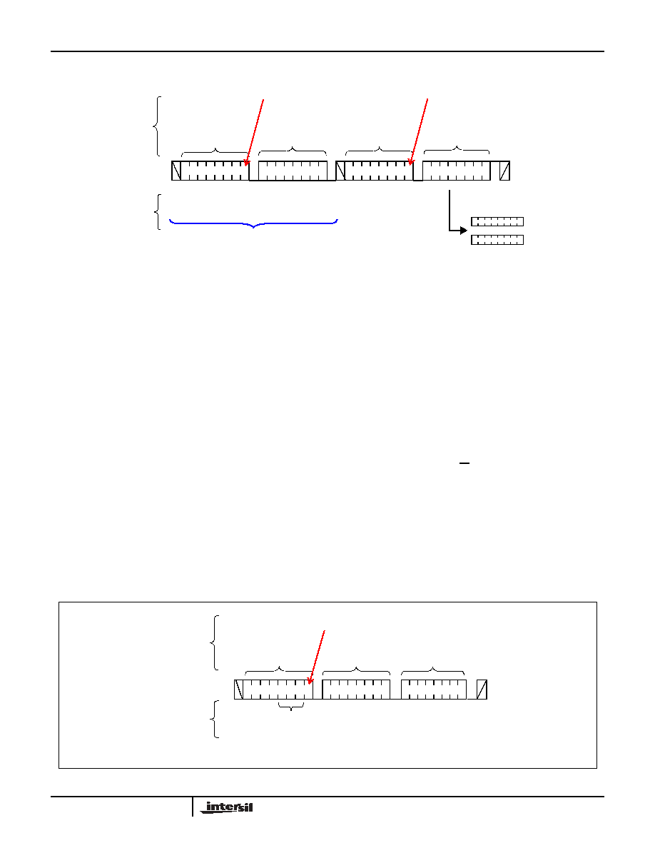
A DCP Read operation allows the user to "read out" the
current "wiper position" of the DCP, as stored in the
associated WCR. This operation is executed using the
Random Address Read command sequence, consisting
of the (DCP) Slave Address Byte followed by an
Instruction Byte and the Slave Address Byte again (Refer
to Figure 10.).
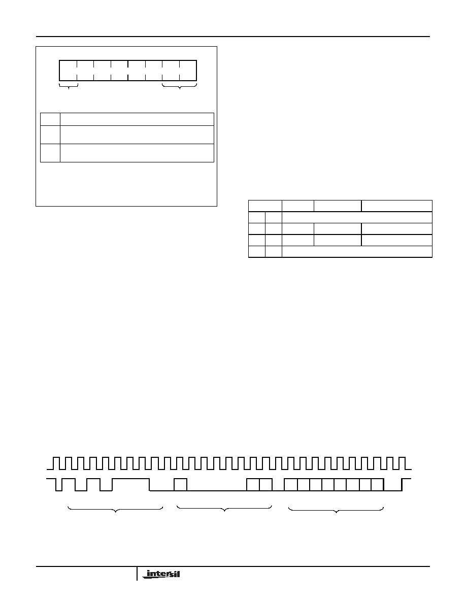
Instruction Byte
While the Slave Address Byte is used to select the DCP
devices, an Instruction Byte is used to determine which
DCP is being addressed.
The Instruction Byte (Figure 8) is valid only when the
Device Type Identifier and the Internal Device Address
bits of the Slave Address are set to 1010111. In this
case, the two Least Significant Bit's (I1 - I0) of the
Instruction Byte are used to select the particular DCP (0
- 2). In the case of a Write to any of the DCPs (i.e. the
LSB of the Slave Address is 0), the Most Significant Bit of
the Instruction Byte (I7), determines the Write Type (WT)
performed.
If WT is "1", then a Nonvolatile Write to the DCP
occurs.
In this case, the "wiper position" of the DCP is changed
by simultaneously writing new data to the associated
Figure 7.
DCP Power-up
t
V1/Vcc
V
TRIP1
V1/Vcc (Max.)
t
purst
Maximum Wiper Recall time
0
t
trans
X9523
8
FN8209.0
March 10, 2005
WCR and NVM. Therefore, the new "wiper position" set-
ting is recalled into the WCR after V1/Vcc of the X9523
has been powered down then powered back up.
If WT is "0" then a DCP Volatile Write is performed. This
operation changes the DCP "wiper position" by writing
new data to the associated WCR only. The contents of
the associated NVM register remains unchanged. There-
fore, when V1/Vcc to the device is powered down then
back up, the "wiper position" reverts to that last written to
the DCP using a nonvolatile write operation.
DCP Write Operation
A write to DCPx (x = 1,2) can be performed using the
three byte command sequence shown in Figure 9.
In order to perform a write operation on a particular DCP,
the Write Enable Latch (WEL) bit of the CONSTAT Reg-
ister must first be set (See "WEL: Write Enable Latch
(Volatile)" on page 10.).
The Slave Address Byte 10101110 specifies that a Write
to a DCP is to be conducted. An ACKNOWLEDGE is
returned by the X9523 after the Slave Address, if it has
been received correctly.
Next, an Instruction Byte is issued on SDA. Bits P1 and
P0 of the Instruction Byte determine which WCR is to be
written, while the WT bit determines if the Write is to be
volatile or nonvolatile. If the Instruction Byte format is
valid, another ACKNOWLEDGE is then returned by the
X9523.
Following the Instruction Byte, a Data Byte is issued to
the X9523 over SDA. The Data Byte contents is latched
into the WCR of the DCP on the first rising edge of the
clock signal, after the LSB of the Data Byte (D0) has
been issued on SDA (See Figure 29).
The Data Byte determines the "wiper position" (which
FET switch of the DCP resistive array is switched ON) of
the DCP. The maximum value for the Data Byte depends
upon which DCP is being addressed (see Table below).
Using a Data Byte larger than the values specified above
results in the "wiper terminal" being set to the highest tap
position. The "wiper position" does NOT roll-over to the
lowest tap position.
For DCP2 (256 Tap), the Data Byte maps one to one to
the "wiper position" of the DCP "wiper terminal". There-
fore, the Data Byte 00001111 (15
10
) corresponds to set-
ting the "wiper terminal" to tap position 15. Similarly, the
Data Byte 00011100 (28
10
) corresponds to setting the
"wiper terminal" to tap position 28. The mapping of the
Data Byte to "wiper position" data for DCP1 (100 Tap), is
shown in "APPENDIX 1". An example of a simple C lan-
guage function which "translates" between the tap posi-
tion (decimal) and the Data Byte (binary) for DCP1, is
given in "APPENDIX 2".
WT
Description
0
Select a Volatile Write operation to be performed
on the DCP pointed to by bits P1 and P0
1
Select a Nonvolatile Write operation to be per-
formed on the DCP pointed to by bits P1 and P0
0
0
WT
0
0
0
P1
P0
WRITE TYPE
DCP SELECT
This bit has no effect when a Read operation is being performed.
I5
I6
I7
I4
I3
I2
I1
I0
Figure 8.
Instruction Byte Format
S
T
A
R
T
1
0
1
0
1
1
1
0
A
C
K
WT
0
0
0
0
0
P1 P0 A
C
K
S
T
O
P
A
C
K
D7 D6 D5 D4 D3 D2 D1 D0
SLAVE ADDRESS BYTE
INSTRUCTION BYTE
DATA BYTE
Figure 9.
DCP Write Command Sequence
P1- P0
DCPx
# Taps
Max. Data Byte
0
0
RESERVED
0
1
x = 1
100
Refer to Appendix 1
1
0
x = 2
256
FFh
1
1
RESERVED
X9523
9
FN8209.0
March 10, 2005
It should be noted that all writes to any DCP of the
X9523 are random in nature. Therefore, the Data
Byte of consecutive write operations to any DCP can
differ by an arbitrary number of bits. Also, setting the
bits P1 = 1, P0 = 1 is a reserved sequence, and will
result in no ACKNOWLEDGE after sending an
Instruction Byte on SDA.
The factory default setting of all "wiper position" settings
is with 00h stored in the NVM of the DCPs. This corre-
sponds to having the "wiper teminal" R
WX
(x = 1,2) at the
"lowest" tap position, Therefore, the resistance between
R
WX
and R
LX
is a minimum (essentially only the Wiper
Resistance, R
W
).
DCP Read Operation
A read of DCPx (x = 1,2) can be performed using the
three byte random read command sequence shown in
Figure 10.
The master issues the START condition and the Slave
Address Byte 10101110 which specifies that a "dummy"
write" is to be conducted. This "dummy" write operation
sets which DCP is to be read (in the preceding Read
operation). An ACKNOWLEDGE is returned by the
X9523 after the Slave Address if received correctly. Next,
an Instruction Byte is issued on SDA. Bits P1-P0 of the
Instruction Byte determine which DCP "wiper position" is
to be read. In this case, the state of the WT bit is "don't
care". If the Instruction Byte format is valid, then another
ACKNOWLEDGE is returned by the X9523.
Following this ACKNOWLEDGE, the master immediately
issues another START condition and a valid Slave
address byte with the R/W bit set to 1. Then the X9523
issues an ACKNOWLEDGE followed by Data Byte, and
finally, the master issues a STOP condition. The Data
Byte read in this operation, corresponds to the "wiper
position" (value of the WCR) of the DCP pointed to by
bits P1 and P0.
Slave
Address
Instruction
Byte
A
C
K
A
C
K
S
t
a
r
t
S
t
o
p
Slave
Address
Data Byte
A
C
K
S
t
a
r
t
SDA Bus
Signals from
the Slave
Signals from
the Master
Figure 10. DCP Read Sequence
"Dummy" write
READ Operation
1 0 1 1 1 1
0
0
0 0 0 0
0
W
T
P
1
P
0
1 0 1 1 1 1
1
0
WRITE Operation
-
MSB
LSB
DCPx
x = 1
x = 2
"-" = DON'T CARE
S
t
a
r
t
S
t
o
p
Slave
Address
Address
Byte
Data
Byte
A
C
K
A
C
K
A
C
K
SDA Bus
Signals from
the Slave
Signals from
the Master
Figure 11. EEPROM Byte Write Sequence
Internal
Device
Address
1 0 1 0 0 0 0
0
WRITE Operation
X9523
10
FN8209.0
March 10, 2005
It should be noted that when reading out the data byte for
DCP1 (100 Tap), the upper most significant bit is an
"unknown". For DCP2 (256 Tap) however, all bits of the
data byte are relevant (See Figure 10).
CONTROL AND STATUS REGISTER
The Control and Status (CONSTAT) Register pro-
vides the user with a mechanism for changing and
reading the status of various parameters of the
X9523 (See Figure 12).
The CONSTAT register is a combination of both volatile
and nonvolatile bits. The nonvolatile bits of the CON-
STAT register retain their stored values even when
V1/Vcc is powered down, then powered back up. The
volatile bits however, will always power-up to a known
logic state "0" (irrespective of their value at power-down).
A detailed description of the function of each of the CON-
STAT register bits follows:
WEL: Write Enable Latch (Volatile)
The WEL bit controls the Write Enable status of the
entire X9523 device. This bit must first be enabled before
ANY write operation (to DCPs, or the CONSTAT regis-
ter). If the WEL bit is not first enabled, then ANY pro-
ceeding (volatile or nonvolatile) write operation to DCPs
or the CONSTAT register, is aborted and no ACKNOWL-
EDGE is issued after a Data Byte.
The WEL bit is a volatile latch that powers up in the dis-
abled, LOW (0) state. The WEL bit is enabled / set by
writing 00000010 to the CONSTAT register. Once
enabled, the WEL bit remains set to "1" until either it is
reset to "0" (by writing 00000000 to the CONSTAT regis-
ter) or until the X9523 powers down, and then up again.
Writes to the WEL bit do not cause an internal high volt-
age write cycle. Therefore, the device is ready for
another operation immediately after a STOP condition is
executed in the CONSTAT Write command sequence
(See Figure 13).
RWEL: Register Write Enable Latch (Volatile)
The RWEL bit controls the (CONSTAT) Register Write
Enable status of the X9523. Therefore, in order to write
to any of the bits of the CONSTAT Register (except
WEL), the RWEL bit must first be set to "1". The RWEL
bit is a volatile bit that powers up in the disabled, LOW
("0") state.
It must be noted that the RWEL bit can only be set, once
the WEL bit has first been enabled (See "CONSTAT
Register Write Operation").
The RWEL bit will reset itself to the default "0" state, in
one of two cases:
--After a successful write operation to any bits of
the CONSTAT register has been completed (See
Figure 13).
--When the X9523 is powered down.
DWLK: DCP Write Lock bit - (Nonvolatile)
The DCP Write Lock bit (DWLK) is used to inhibit a DCP
write operation (changing the "wiper position").
When the DCP Write Lock bit of the CONSTAT register
is set to "1", then the "wiper position" of the DCPs can-
not be changed - i.e. DCP write operations cannot be
conducted:
The factory default setting for this bit is DWLK = 0.
IMPORTANT NOTE: If the Write Protect (WP) pin of the
X9523 is active (HIGH), then nonvolatile write operations
to the DCPs are inhibited, irrespective of the DCP Write
Lock bit setting (See "WP: Write Protection Pin").
Bit(s)
Description
POR1
Power-on Reset bit
V2OS
V2 Output Status flag
V1OS
V1 Output Status flag
CS4
Always set to "0" (RESERVED)
DWLK
Sets the DCP Write Lock
RWEL
Register Write Enable Latch bit
WEL
Write Enable Latch bit
POR0
Power-on Reset bit
POR1
WEL
POR0
CS5
CS6
CS7
CS4
CS3
CS2
CS1
CS0
V3OS
V2OS
DWLK
0
RWEL
Figure 12. CONSTAT Register Format
NV
NV
NV
NOTE: Bits labelled NV are nonvolatile (See "CONTROL AND STATUS REGISTER").
DWLK
DCP Write Operation Permissible
0
YES (Default)
1
NO
X9523
11
FN8209.0
March 10, 2005
POR1, POR0: Power-on Reset bits - (Nonvolatile)
Applying voltage to V
CC
activates the Power-on Reset
circuit which holds V1RO output HIGH, until the supply
voltage stabilizes above the V
TRIP1
threshold for a
period of time, t
PURST
(See Figure 25).
The Power-on Reset bits, POR1 and POR0 of the
CONSTAT register determine the tPURST delay time of
the Power-on Reset circuitry (See "VOLTAGE MONI-
TORING FUNCTIONS"). These bits of the CONSTAT
register are nonvolatile, and therefore power-up to the
last written state.
The nominal Power-on Reset delay time can be selected
from the following table, by writing the appropriate bits to
the CONSTAT register:
The default for these bits are POR1 = 0, POR0 = 1.
V2OS, V3OS: Voltage Monitor Status Bits (Volatile)
Bits V2OS and V3OS of the CONSTAT register are
latched, volatile flag bits which indicate the status of the
Voltage Monitor reset output pins V2RO and V3RO.
At power-up the VxOS (x = 2,3) bits default to the value
"0". These bits can be set to a "1" by writing the appropri-
ate value to the CONSTAT register. To provide consis-
tency between the VxRO and VxOS however, the status
of the VxOS bits can only be set to a "1" when the corre-
sponding VxRO output is HIGH.
Once the VxOS bits have been set to "1", they will be
reset to "0" if:
--The device is powered down, then back up,
--The corresponding VxRO output becomes LOW.
CONSTAT Register Write Operation
The CONSTAT register is accessed using the Slave
Address set to 1010010 (Refer to Figure 4.). Following
the Slave Address Byte, access to the CONSTAT regis-
ter requires an Address Byte which must be set to FFh.
Only one data byte is allowed to be written for each
CONSTAT register Write operation. The user must issue
a STOP, after sending this byte to the register, to initiate
the nonvolatile cycle that stores the DWLK, POR1 and
POR0 bits. The X9523 will not ACKNOWLEDGE any
data bytes written after the first byte is entered (Refer to
Figure 13.).
When writing to the CONSTAT register, the bit CS4 must
always be set to "0". Writing a "1" to bit CS4 of the CON-
STAT register is a reserved operation.
Prior to writing to the CONSTAT register, the WEL and
RWEL bits must be set using a two step process, with
the whole sequence requiring 3 steps
--Write a 02H to the CONSTAT Register to set the Write
Enable Latch (WEL). This is a volatile operation, so
there is no delay after the write. (Operation preceded
by a START and ended with a STOP).
--Write a 06H to the CONSTAT Register to set the Reg-
ister Write Enable Latch (RWEL) AND the WEL bit.
This is also a volatile cycle. The zeros in the data byte
are required. (Operation preceded by a START and
ended with a STOP).
POR1
POR0
Power-on Reset delay (t
PUV1RO
)
0
0
50ms
0
1
100ms (Default)
1
0
200ms
1
1
300ms
S
T
A
R
T
1
0
1
0
0
1
0
R/W A
C
K
1
1
1
1
1
1
1
1
A
C
K
SCL
SDA
S
T
O
P
A
C
K
CS7 CS6 CS5 CS4 CS3 CS2 CS1 CS0
SLAVE ADDRESS BYTE
ADDRESS BYTE
CONSTAT REGISTER DATA IN
Figure 13. CONSTAT Register Write Command Sequence
X9523
12
FN8209.0
March 10, 2005
--Write a one byte value to the CONSTAT Register that
has all the bits set to the desired state. The CONSTAT
register can be represented as qxyst01r in binary,
where xy are the Voltage Monitor Output Status
(V2OS and V3OS) bits, t is the DCP Write Lock
(DWLK) bit, and qr are the Power-on Reset delay time
(t
PUV1RO
) control bits (POR1 - POR0). This operation
is proceeded by a START and ended with a STOP bit.
Since this is a nonvolatile write cycle, it will typically
take 5ms to complete. The RWEL bit is reset by this
cycle and the sequence must be repeated to change
the nonvolatile bits again. If bit 2 is set to `1' in this third
step (qxys t11r) then the RWEL bit is set, but the
V2OS, V3OS, POR1, POR0, and DWLK bits remain
unchanged. Writing a second byte to the control regis-
ter is not allowed. Doing so aborts the write operation
and the X9523 does not return an ACKNOWLEDGE.
For example, a sequence of writes to the device CON-
STAT register consisting of [02H, 06H, 02H] will reset all
of the nonvolatile bits in the CONSTAT Register to "0".
It should be noted that a write to any nonvolatile bit of
CONSTAT register will be ignored if the Write Protect
pin of the X9523 is active (HIGH) (See "WP: Write
Protection Pin").
CONSTAT Register Read Operation
The contents of the CONSTAT Register can be read at
any time by performing a random read (See Figure 14).
Using the Slave Address Byte set to 10100101, and an
Address Byte of FFh. Only one byte is read by each reg-
ister read operation. The X9523 resets itself after the first
byte is read. The master should supply a STOP condition
to be consistent with the bus protocol.
After setting the WEL and / or the RWEL bit(s) to a "1",
a CONSTAT register read operation may occur, without
interrupting a proceeding CONSTAT register write
operation.
When performing a read operation on the CONSTAT
registerm, bit CS4 will always return a "0" value.
DATA PROTECTION
There are a number of levels of data protection fea-
tures designed into the X9523. Any write to the device
first requires setting of the WEL bit in the CONSTAT
register. A write to the CONSTAT register itself, further
requires the setting of the RWEL bit. DCP Write Lock
protection of the device enables the user to inhibit
writes to all the DCPs. One further level of data protec-
tion in the X9523, is incorporated in the form of the
Write Protection pin.
X9522 Write Permission Status
Figure 14. CONSTAT Register Read Command Sequence
0
Slave
Address
Address
Byte
A
C
K
A
C
K
S
t
a
r
t
S
t
o
p
Slave
Address
Data
A
C
K
1
S
t
a
r
t
SDA Bus
Signals from
the Slave
Signals from
the Master
0 1 0 0 1 0
1
1
0 1 0 0 1 0
WRITE Operation
"Dummy" Write
READ Operation
CS7 ... CS0
DWLK
(DCP Write Lock
bit status)
WP
(Write Protect pin
status)
DCP Volatile Write
Permitted
DCP Nonvolatile
Write Permitted
Write to CONSTAT Register
Permitted
Volatile Bits
Nonvolatile Bits
1
1
NO
NO
NO
NO
0
1
YES
NO
NO
NO
1
0
NO
NO
YES
YES
0
0
YES
YES
YES
YES
X9523

13
FN8209.0
March 10, 2005
WP: Write Protection Pin
When the Write Protection (WP) pin is active (HIGH), it
disables nonvolatile write operations to the X9523.
The table below (X9523 Write Permission Status) sum-
marizes the effect of the WP pin (and DCP Write Lock),
on the write permission status of the device.
Additional Data Protection Features
In addition to the preceding features, the X9523 also
incorporates the following data protection functionality:
--The proper clock count and data bit sequence is
required prior to the STOP bit in order to start a nonvol-
atile write cycle.
VOLTAGE MONITORING FUNCTIONS
V1 / Vcc Monitoring
The X9523 monitors the supply voltage and drives the
V1RO output HIGH (using an external "pull up" resistor)
if V1/Vcc is lower than V
TRIP1
threshold. The V1RO
output will remain HIGH until V1/Vcc exceeds V
TRIP1
for a minimum time of t
PURST
. After this time, the
V1RO pin is driven to a LOW state. See Figure 25.
For the Power-on/Low Voltage Reset function of the
X9523, the V1RO output may be driven HIGH down to a
V1/Vcc of 1V (V
RVALID
). See Figure 25. Another feature
of the X9523, is that the value of t
PURST
may be selected
in software via the CONSTAT register (See "POR1,
POR0: Power-on Reset bits - (Nonvolatile)" on page 11.).
It is recommended to stop communication to the device
while while V1RO is HIGH. Also, setting the Manual
Reset (MR) pin HIGH overrides the Power-on/Low
Voltage circuitry and forces the V1RO output pin HIGH
(See "Manual Reset").
Manual Reset
The V1RO output can be forced HIGH externally using
the Manual Reset (MR) input. MR is a de-bounced, TTL
compatible input, and so it may be operated by connect-
ing a push-button directly from V1/Vcc to the MR pin.
V1RO remains HIGH for time t
PURST
after MR has
returned to its LOW state (See Figure 15). An external
"pull down" resistor is required to hold this pin (nor-
mally) LOW.
V2 monitoring
The X9523 asserts the V2RO output HIGH if the volt-
age V2 exceeds the corresponding V
TRIP2
threshold
(See Figure 16). The bit V2OS in the CONSTAT regis-
ter is then set to a "0" (assuming that it has been set to
"1" after system initilization).
The V2RO output may remain active HIGH with V
CC
down to 1V.
V3 monitoring
The X9523 asserts the V3RO output HIGH if the volt-
age V3 exceeds the corresponding V
TRIP3
threshold
(See Figure 16). The bit V3OS in the CONSTAT regis-
ter is then set to a "0" (assuming that it has been set to
"1" after system initilization).
The V3RO output may remain active HIGH with V
CC
down to 1V.
MR
V1RO
V1 / Vcc
0 Volts
0 Volts
t
PURST
Figure 15. Manual Reset Response
0 Volts
V
TRIP1
Figure 16. Voltage Monitor Response
Vx
VxRO
0V
0V
V
TRIPx
(x = 2,3)
0 Volts
V
TRIP1
V1 / Vcc
X9523
14
FN8209.0
March 10, 2005
V
TRIPX
THRESHOLDS (X = 1,2,3)
The X9523 is shipped with pre-programmed threshold
(V
TRIPx
) voltages. In applications where the required
thresholds are different from the default values, or if a
higher precision/tolerance is required, the X9523 trip
points may be adjusted by the user, using the steps
detailed below.
Setting a V
TRIPx
Voltage (x = 1,2,3)
There are two procedures used to set the threshold
voltages (V
TRIPx
), depending if the threshold voltage
to be stored is higher or lower than the present value.
For example, if the present V
TRIPx
is 2.9 V and the
new V
TRIPx
is 3.2 V, the new voltage can be stored
directly into the V
TRIPx
cell. If however, the new setting
is to be lower than the present setting, then it is neces-
sary to "reset" the V
TRIPx
voltage before setting the
new value.
Setting a Higher V
TRIPx
Voltage (x = 1,2,3)
To set a V
TRIPx
threshold to a new voltage which is
higher than the present threshold, the user must apply
the desired V
TRIPx
threshold voltage to the corre-
sponding input pin (V1/Vcc, V2 or V3). Then, a pro-
gramming voltage (Vp) must be applied to the WP pin
before a START condition is set up on SDA. Next, issue
on the SDA pin the Slave Address A0h, followed by
the Byte Address 01h for V
TRIP1
, 09h for V
TRIP2
, and
0Dh for V
TRIP3
, and a 00h Data Byte in order to pro-
gram V
TRIPx
. The STOP bit following a valid write
operation initiates the programming sequence. Pin WP
must then be brought LOW to complete the operation
(See Figure 18). The user does not have to set the
WEL bit in the CONSTAT register before performing
this write sequence.
0 1 2 3 4 5 6 7
SCL
SDA
A0h
0 1 2 3 4 5 6 7
WP
V
P
0 1 2 3 4 5 6 7
V
TRIPx
V2, V3
01h
sets V
TRIP1
Figure 17. Setting V
TRIPx
to a higher level (x = 1,2,3).
09h
sets V
TRIP2
0Dh
sets V
TRIP3
Data Byte
V1 / Vcc
00h
S
T
A
R
T
All others Reserved.
SDA
A0h
0 1 2 3 4 5 6 7
SCL
0 1 2 3 4 5 6 7
WP
V
P
0 1 2 3 4 5 6 7
Figure 18. Resetting the V
TRIPx
Level
03h
Resets
VTRIP1
0Bh
Resets
VTRIP2
0Fh
Resets
VTRIP3
Data Byte
00h
S
T
A
R
T
All others Reserved.
X9523

15
FN8209.0
March 10, 2005
Setting a Lower V
TRIPx
Voltage (x = 1,2,3).
In order to set V
TRIPx
to a lower voltage than the
present value, then V
TRIPx
must first be "reset" accord-
ing to the procedure described below. Once V
TRIPx
has been "reset", then V
TRIPx
can be set to the desired
voltage using the procedure described in "Setting a
Higher V
TRIPx
Voltage".
Resetting the V
TRIPx
Voltage (x = 1,2,3).
To reset a V
TRIPx
voltage, apply the programming volt-
age (Vp) to the WP pin before a START condition is set
up on SDA. Next, issue on the SDA pin the Slave
Address A0h followed by the Byte Address 03h for
V
TRIP1
, 0Bh for V
TRIP2
, and 0Fh for V
TRIP3
, followed
by 00h for the Data Byte in order to reset V
TRIPx
. The
STOP bit following a valid write operation initiates the
programming sequence. Pin WP must then be brought
LOW to complete the operation (See Figure 18).The
user does not have to set the WEL bit in the CON-
STAT register before performing this write sequence.
After being reset, the value of V
TRIPx
becomes a nomi-
nal value of 1.7V.
V
TRIPx
Accuracy (x = 1,2,3).
The accuracy with which the V
TRIPx
thresholds are set,
can be controlled using the iterative process shown in
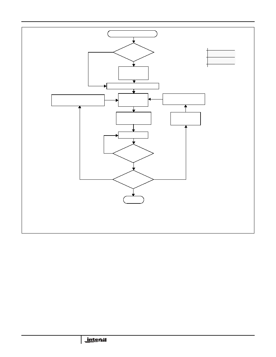
Figure 19.
If the desired threshold is less that the present threshold
voltage, then it must first be "reset" (See "Resetting the
VTRIPx Voltage (x = 1,2,3)." ) .
The desired threshold voltage is then applied to the
appropriate input pin (V1/Vcc, V2 or V3) and the proce-
dure described in Section "Setting a Higher V
TRIPx
Voltage" must be followed.
Once the desired V
TRIPx
threshold has been set, the
error between the desired and (new) actual set threshold
can be determined. This is achieved by applying V1/Vcc
to the device, and then applying a test voltage higher
than the desired threshold voltage, to the input pin of the
voltage monitor circuit whose V
TRIPx
was programmed.
For example, if V
TRIP2
was set to a desired level of 3.0V,
then a test voltage of 3.4 V may be applied to the voltage
monitor input pin V2. In the case of setting of V
TRIP1
then
only V1/Vcc need be applied. In all cases, care should be
taken not to exceed the maximum input voltage limits.
After applying the test voltage to the voltage monitor
input pin, the test voltage can be decreased (either in dis-
crete steps, or continuously) until the output of the volt-
age monitor circuit changes state. At this point, the error
between the actua measured, and desired threshold lev-
els is calculated.
For example, the desired threshold for V
TRIP2
is set to
3.0V, and a test voltage of 3.4V was applied to the input
pin V2 (after applying power to V1/Vcc). The input volt-
age is decreased, and found to trip the associated output
level of pin V2RO from a LOW to a HIGH, when V2
reaches 3.09V. From this, it can be calculated that the
programming error is 3.09 - 3.0 = 0.09V.
If the error between the desired and measured V
TRIPx
is
less than the maximum desired error, then the program-
ming process may be terminated. If however, the error is
greater than the maximum desired error, then another
iteration of the V
TRIPx
programming sequence can be
performed (using the calculated error) in order to further
increase the accuracy of the threshold voltage.
If the calculated error is greater than zero, then the
V
TRIPx
must first be "reset", and then programmed to the
a value equal to the previously set V
TRIPx
minus the cal-
culated error. If it is the case that the error is less than
zero, then the V
TRIPx
must be programmed to a value
equal to the previously set V
TRIPx
plus the absolute value
of the calculated error.
Continuing the previous example, we see that the calcu-
lated error was 0.09V. Since this is greater than zero, we
must first "reset" the V
TRIP2
threshold, then apply a volt-
age equal to the last previously programmed voltage,
minus the last previously calculated error. Therefore, we
must apply V
TRIP2
= 2.91 V to pin V2 and execute the
programming sequence (See "Setting a Higher VTRIPx
Voltage (x = 1,2,3)" ) .
Using this process, the desired accuracy for a particu-
lar V
TRIPx
threshold may be attained using a succes-
sive number of iterations.
X9523
16
FN8209.0
March 10, 2005
V
TRIPx
Programming
Apply Vcc & Voltage
Decrease Vx
switches?
Actual
V
TRIPx
-
Desired
V
TRIPx
DONE
Execute
Sequence
V
TRIPx
Reset
Set Vx = desired
V
TRIPx
Execute
Sequence
Set Higher
V
TRIPx
New Vx applied =
Old Vx applied
+
| Error |
Execute
Sequence
Reset
V
TRIPx
New Vx applied =
Old Vx applied
-
| Error |
Error < MDE
≠
| Error | < | MDE |
YES
NO
Error >MDE
+
NO
YES
Figure 19. V
TRIPx
Setting / Reset Sequence (x = 1,2,3)
> Desired
V
TRIPx
to Vx
Desired V
TRIPx
<
present value?
Note: X = 1,2,3.
Let: MDE = Maximum Desired Error
Output
Acceptable
Error Range
MDE
+
MDE
≠
Error = Actual ≠ Desired
= Error
Desired Value
X9523
17
FN8209.0
March 10, 2005
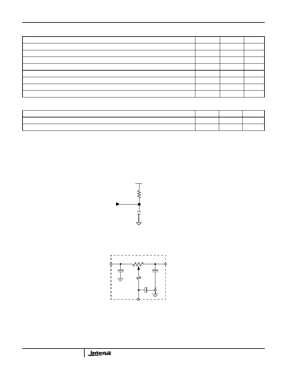
ABSOLUTE MAXIMUM RATINGS
RECOMMENDED OPERATING CONDITIONS
NOTE: Stresses above those listed under "Absolute Maximum Ratings" may cause permanent damage to the device. This
is a stress rating only and the functional operation of the device at these or any other conditions above those listed in the
operational sections of this specification is not implied. Exposure to absolute maximum rating conditions for extended peri-
ods may affect device reliability
Figure 20. Equivalent A.C. Circuit
Figure 21. DCP SPICE Macromodel
Parameter
Min.
Max.
Units
Temperature under Bias
-65
+135
∞C
Storage Temperature
-65
+150
∞C
Voltage on WP pin (With respect to Vss)
-1.0
+15
V
Voltage on other pins (With respect to Vss)
-1.0
+7
V
| Voltage on R
Hx
- Voltage on R
Lx
|
(x = 0,1,2.
Referenced to Vss
)
V1/Vcc
V
D.C. Output Current (SDA,V1RO,V2RO,V3RO)
0
5
mA
Lead Temperature (Soldering, 10 seconds)
300
∞C
Supply Voltage Limits (Applied V1/Vcc voltage, referenced to Vss)
2.7
5.5
V
Temperature
Min.
Max.
Units
Commercial
0
70
∞C
Industrial
-40
+85
∞C
V1 / Vcc = 5V
V2RO
100pF
SDA
2300
V3RO
V1RO
C
H
C
L
R
Wx
10pF
10pF
R
Hx
R
Lx
R
TOTAL
C
W
25pF
R
W
(x=0,1,2)
X9523
18
FN8209.0
March 10, 2005
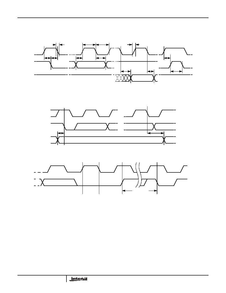
TIMING DIAGRAMS
Figure 22. Bus Timing
Figure 23. WP Pin Timing
Figure 24. Write Cycle Timing
t
SU:STO
t
DH
t
HIGH
t
SU:STA
t
HD:STA
t
HD:DAT
t
SU:DAT
SCL
SDA IN
SDA OUT
t
F
t
LOW
t
BUF
t
AA
t
R
t
HD:WP
SCL
SDA IN
WP
t
SU:WP
Clk 1
Clk 9
START
SCL
SDA
t
WC
8th bit of last byte
ACK
Stop
Condition
Start
Condition
X9523

19
FN8209.0
March 10, 2005
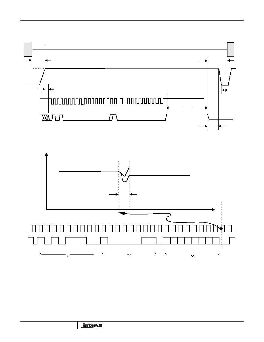
Figure 25. Power-Up and Power-Down Timing
Figure 26. Manual Reset Timing Diagram
Figure 27. V2, V3 Timing Diagram
V1/Vcc
t
PURST
tR
tF
0 Volts
V TRIP1
V1RO
t
RPD
0 Volts
t
PURST
MR
0 Volts
0 Volts
MR
V1RO
t PURST
t
MRD
0 Volts
V1 / Vcc
V1/Vcc
V TRIP1
t
MRPW
Vx
t Rx
t
Fx
V TRIPx
V
RVALID
VxRO
t
RPDx
0 Volts
Note : x = 2,3.
0 Volts
0 Volts
t
RPDx
t
RPDx
t
RPDx
V TRIP1
V1/Vcc
X9523
20
FN8209.0
March 10, 2005
Figure 28. V
TRIPX
Programming Timing Diagram (x = 1,2,3).
Figure 29. DCP "Wiper Position" Timing
WP
t
VPS
V
P
t
VPO
SCL
SDA
t
wc
t
TSU
t
THD
V Vcc, V2, V3
V
TRIPx
00h
t
VPH
NOTE : V1/Vcc must be greater than V2, V3 when programming.
S
T
A
R
T
1
0
1
0
1
1
1
0
A
C
K
WT
0
0
0
0
0
P1 P0 A
C
K
S
T
O
P
A
C
K
D7 D6 D5 D4 D3 D2 D1 D0
SLAVE ADDRESS BYTE
INSTRUCTION BYTE
DATA BYTE
SCL
SDA
Time
Rwx (x = 0,1,2)
t
wr
R
wx(n + 1)
R
wx(n - 1)
R
wx(n)
n = tap position
X9523

21
FN8209.0
March 10, 2005
D.C. OPERATING CHARACTERISTICS
Notes: 1. The device enters the Active state after any START, and remains active until: 9 clock cycles later if the Device Select Bits in the Slave
Address Byte are incorrect; 200nS after a STOP ending a read operation; or t
WC
after a STOP ending a write operation.
Notes: 2. The device goes into Standby: 200nS after any STOP, except those that initiate a high voltage write cycle; tWC after a STOP that initiates a
high voltage cycle; or 9 clock cycles after any START that is not followed by the correct Device Select Bits in the Slave Address Byte.
Notes: 3. Current through external pull up resistor not included.
Notes: 4.
V
IN
= Voltage applied to input pin.
Notes: 5.
V
OUT
= Voltage applied to output pin.
Notes: 6. See "ORDERING INFORMATION" on page 30.
Notes: 7. V
IL
Min. and V
IH
Max. are for reference only and are not tested
Symbol
Parameter
Min
Typ
Max
Unit
Test Conditions / Notes
I
CC1
(1)
Current into V
CC
Pin
(X9523: Active)
Read memory array
(3)
Write nonvolatile memory
0.4
1.5
mA
f
SCL
= 400kHz
I
CC2
(2)
Current into V
CC
Pin
(X9523:Standby)
With 2-Wire bus activity
(3)
No 2-Wire bus activity
50
50
µ
A
V
SDA
= V
CC
MR = Vss
WP = Vss or Open/Floating
V
SCL
= V
CC
(when no bus activity
else f
SCL
= 400kHz)
I
LI
Input Leakage Current (SCL, SDA, MR)
0.1
10
µ
A
V
IN
(4)
= GND to V
CC.
Input Leakage Current (WP)
10
µ
A
I
ai
Analog Input Leakage
1
10
µA
V
IN
= V
SS
to V
CC
with all other an-
alog pins floating
I
LO
Output Leakage Current (SDA, V1RO,
V2RO, V3RO)
0.1
10
µ
A
V
OUT
(5)
= GND to V
CC.
X9523 is in Standby
(2)
V
TRIP1PR
V
TRIP1
Programming Range
2.75
4.70
V
V
TRIPxPR
V
TRIPx
Programming Range (x = 2,3)
1.8
4.70
V
V
TRIP1
(6)
Pre - programmed V
TRIP1
threshold
2.85
4.55
3.0
4.7
3.05
4.75
V
Factory shipped default option A
Factory shipped default option B
V
TRIP2
(6)
Pre - programmed V
TRIP2
threshold
1.65
2.85
1.8
3.0
1.85
3.05
V
Factory shipped default option A
Factory shipped default option B
V
TRIP3
(6)
Pre - programmed V
TRIP3
threshold
1.65
2.85
1.8
3.0
1.85
3.05
V
Factory shipped default option A
Factory shipped default option B
I
Vx
V2 Input leakage current
V3 Input leakage current
1
1
µ
A
V
SDA
= V
SCL
= V
CC
Others=GND or V
CC
V
IL
(7)
Input LOW Voltage (SCL, SDA, WP, MR)
-0.5
0.8
V
V
IH
(7)
Input HIGH Voltage (SCL,SDA, WP, MR)
2.0
V
CC
+0.5
V
V
OLx
V1RO, V2RO, V3RO, SDA Output Low
Voltage
0.4
V
I
SINK
= 2.0mA
X9523
22
FN8209.0
March 10, 2005
A.C. CHARACTERISTICS (See Figure 22, Figure 23, Figure 24)
A.C. TEST CONDITIONS
NONVOLATILE WRITE CYCLE TIMING
CAPACITANCE (T
A
= 25∞C, F = 1.0 MHZ, V
CC
= 5V)
Notes: 1. Typical values are for T
A
= 25∞C and V
CC
= 5.0V
Notes: 2. Cb = total capacitance of one bus line in pF.
Notes: 3. Over recommended operating conditions, unless otherwise specified
Notes: 4. t
WC
is the time from a valid STOP condition at the end of a write sequence to the end of the self-timed internal nonvolatile write cycle. It is
the minimum cycle time to be allowed for any nonvolatile write by the user, unless Acknowledge Polling is used.
Notes: 5. This parameter is not 100% tested.
Symbol Parameter
400kHz
Min
Max
Units
f
SCL
SCL Clock Frequency
0
400
kHz
t
IN
(5)
Pulse width Suppression Time at inputs
50
ns
t
AA
(5)
SCL LOW to SDA Data Out Valid
0.1
0.9
µ
s
t
BUF
(5)
Time the bus free before start of new transmission
1.3
µ
s
t
LOW
Clock LOW Time
1.3
µ
s
t
HIGH
Clock HIGH Time
0.6
µ
s
t
SU:STA
Start Condition Setup Time
0.6
µ
s
t
HD:STA
Start Condition Hold Time
0.6
µ
s
t
SU:DAT
Data In Setup Time
100
ns
t
HD:DAT
Data In Hold Time
0
µ
s
t
SU:STO
Stop Condition Setup Time
0.6
µ
s
t
DH
(5)
Data Output Hold Time
50
ns
t
R
(5)
SDA and SCL Rise Time
20 +.1Cb
(2)
300
ns
t
F
(5)
SDA and SCL Fall Time
20 +.1Cb
(2)
300
ns
t
SU:WP
WP Setup Time
0.6
µ
s
t
HD:WP
WP Hold Time
0
µ
s
Cb
(5)
Capacitive load for each bus line
400
pF
Input Pulse Levels
0.1V
CC
to 0.9V
CC
Input Rise and Fall Times
10ns
Input and Output Timing Levels
0.5V
CC
Output Load
See Figure 20
Symbol Parameter
Min.
Typ.(1)
Max.
Units
t
WC
(4)
Nonvolatile Write Cycle Time
5
10
ms
Symbol
Parameter
Max
Units
Test Conditions
C
OUT
(5)
Output Capacitance (SDA, V1RO, V2RO, V3RO)
8
pF
V
OUT
= 0V
C
IN
(5)
Input Capacitance (SCL, WP, MR)
6
pF
V
IN
= 0V
X9523
23
FN8209.0
March 10, 2005
POTENTIOMETER CHARACTERISTICS
Notes: 1. Power Rating between the wiper terminal R
WX(n)
and the end terminals R
HX
or R
LX
- for ANY tap position n, (x = 0,1,2).
Notes: 2. Absolute Linearity is utilized to determine actual wiper resistance versus, expected resistance = (R
wx(n)
(actual) - R
wx(n)
(expected)) = ±1
Ml Maximum (x = 0,1,2).
Notes: 3. Relative Linearity is a measure of the error in step size between taps = R
Wx(n+1)
- [R
wx(n)
+ Ml] = ±1 Ml (x = 0,1,2)
Notes: 4. 1 Ml = Minimum Increment = R
TOT
/ (Number of taps in DCP - 1).
Notes: 5. Typical values are for T
A
= 25∞C and nominal supply voltage.
Notes: 6. This parameter is periodically sampled and not 100% tested.
Symbol
Parameter
Limits
Test Conditions/Notes
Min.
Typ.
Max.
Units
R
TOL
End to End Resistance Tolerance
-20
+20
%
V
RHx
R
H
Terminal Voltage (x = 0,1,2)
Vss
V
CC
V
V
RLx
R
L
Terminal Voltage (x = 0,1,2)
Vss
V
CC
V
P
R
Power Rating
(1)(6)
10
mW
R
TOTAL
= 10k
(
DCP0, DCP1)
5
mW
R
TOTAL
= 100k
(
DCP2)
R
W
DCP Wiper Resistance
200
400
I
W
= 1mA, V
CC
= 5V, V
RHx
= Vcc,
V
RLx
= Vss (x = 0,1,2).
400
1200
I
W
= 1mA, V
CC
= 2.7V,
V
RHx
= Vcc, V
RLx
= Vss
(x = 0,1,2)
I
W
Wiper Current
(6)
4.4
mA
Noise
mV/
sqt(Hz)
R
TOTAL
= 10k
(
DCP0, DCP1)
mV/
sqt(Hz)
R
TOTAL
= 100k
(
DCP2)
Absolute Linearity
(2)
-1
+1
MI
(4)
R
w(n)(actual)
- R
w(n)(expected)
Relative Linearity
(3)
-1
+1
MI
(4)
R
w(n + 1)
- [R
w(n) + MI
]
R
TOTAL
Temperature Coefficient
±300
ppm/∞C
R
TOTAL
= 10k
(
DCP0, DCP1)
±300
ppm/∞C
R
TOTAL
= 100k
(
DCP2)
C
H
/C
L
/C
W
Potentiometer Capacitances
10/10/25
pF
See Figure 21.
t
wr
Wiper Response time
(6)
200
µ
s
See Figure 29.
X9523
24
FN8209.0
March 10, 2005
V
TRIPX
(X = 1,2,3) PROGRAMMING PARAMETERS (See Figure 28)
Notes:
The above parameters are not 100% tested.
V1RO, V2RO, V3RO OUTPUT TIMING. (See Figure 25, Figure 26, Figure 27)
Notes: 1. See Figure 26 for timing diagram.
Notes: 2. See Figure 20 for equivalent load.
Notes: 3. This parameter describes the lowest possible V1/Vcc level for which the outputs V1RO, V2RO, and V3RO will be correct with respect to
their inputs (V1/Vcc, V2, V3).
Notes: 4. From MR rising edge crossing V
IH
, to V1RO rising edge crossing V
OH
.
Notes: 5. The above parameters are not 100% tested.
Parameter
Description
Min
Typ
Max
Units
t
VPS
V
TRIPx
Program Enable Voltage Setup time
10
µ
s
t
VPH
V
TRIPx
Program Enable Voltage Hold time
10
µ
s
t
TSU
V
TRIPx
Setup time
10
µ
s
t
THD
V
TRIPx
Hold (stable) time
10
µ
s
t
VPO
V
TRIPx
Program Enable Voltage Off time
(Between successive adjustments)
1
ms
t
wc
V
TRIPx
Write Cycle time
5
10
ms
V
P
Programming Voltage
10
15
V
V
ta
V
TRIPx
Program Voltage accuracy
(Programmed at 25
o
C.)
-100
+100
mV
V
tv
V
TRIP
Program variation after programming (-40 - 85
o
C).
(Programmed at 25
o
C.)
-25
+10
+25
mV
Symbol
Description
Condition
Min.
Typ.
Max.
Units
t
PURST
(5)
Power-on Reset delay time
POR1 = 0, POR0 = 0
25
50
75
ms
POR1 = 0, POR0 = 1
50
100
150
ms
POR1 = 1, POR0 = 0
100
200
300
ms
POR1 = 1, POR0 = 1
150
300
450
ms
t
MRD
(26)(2)(5)
MR to V1RO propagation delay
See
(1)(2)(4)
5
µ
s
t
MRDPW
(5)
MR pulse width
500
ns
t
RPDx
(5)
V Vcc, V2, V3 to V1RO, V2RO,
V3RO propagation
delay (respectively)
20
µ
s
t
Fx
(5)
V1/Vcc, V2, V3 Fall Time
20
mV/
µ
s
t
Rx
(5)
V1/Vcc, V2, V3 Rise Time
20
mV/
µ
s
V
RVALID
(5)
V1/Vcc for V1RO, V2RO, V3RO
Valid
(3)
.
1
V
X9523

25
FN8209.0
March 10, 2005
APPENDIX 1
DCP1 (100 Tap) Tap position to Data Byte translation Table
Tap
Position
Data Byte
Decimal
Binary
0
0
0000 0000
1
1
0000 0001
.
.
.
.
.
.
23
23
0001 0111
24
24
0001 1000
25
56
0011 1000
26
55
0011 0111
.
.
.
.
.
.
48
33
0010 0001
49
32
0010 0000
50
64
0100 0000
51
65
0100 0001
.
.
.
.
.
.
73
87
0101 0111
74
88
0101 1000
75
120
0111 1000
76
119
0111 0111
.
.
.
.
.
.
98
97
0110 0001
99
96
0110 0000
X9523

26
FN8209.0
March 10, 2005
APPENDIX 2
DCP1 (100 Tap) tap position to Data Byte translation algorithm example. (Example 1)
unsigned DCP1_TAP_Position(int tap_pos)
{
int block;
int i;
int offset;
int wcr_val;
offset= 0;
block = tap_pos / 25;
if (block < 0) return ((unsigned)0);
else if (block <= 3)
{
switch(block)
{
case (0): return ((unsigned)tap_pos) ;
case (1):
{
wcr_val = 56;
offset = tap_pos - 25;
for (i=0; i<= offset; i++) wcr_val-- ;
return ((unsigned)++wcr_val);
}
case (2):
{
wcr_val = 64;
offset = tap_pos - 50;
for (i=0; i<= offset; i++) wcr_val++ ;
return ((unsigned)--wcr_val);
}
case (3):
{
wcr_val = 120;
offset = tap_pos - 75;
for (i=0; i<= offset; i++) wcr_val-- ;
return ((unsigned)++wcr_val);
}
}
}
return((unsigned)01100000);
}
X9523

27
FN8209.0
March 10, 2005
APPENDIX 2
DCP1 (100 Tap) tap position to Data Byte translation algorithm example. (Example 2)
unsigned DCP100_TAP_Position(int tap_pos)
{
/* optional range checking
*/ if (tap_pos < 0) return ((unsigned)0); /* set to min val */
else if (tap_pos >99) return ((unsigned) 96); /* set to max val */
/* 100 Tap DCP encoding formula */
if (tap_pos > 74)
return ((unsigned) (195 - tap_pos));
else if (tap_pos > 49)
return ((unsigned) (14 + tap_pos));
else if (tap_pos > 24)
return ((unsigned) (81 - tap_pos));
else return (tap_pos);
}
X9523
28
FN8209.0
March 10, 2005
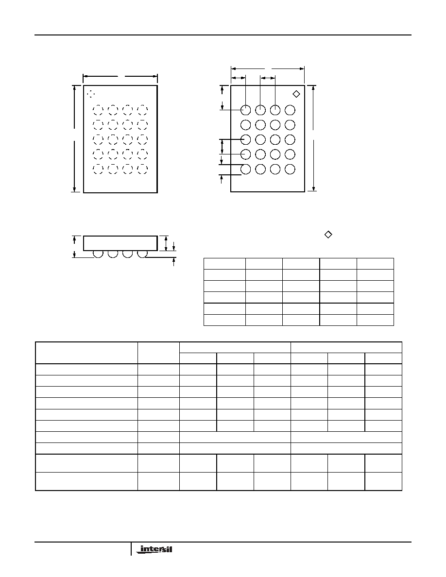
20 Ball BGA (X9523)
a
B
A
D
C
E
1
2
3
4
B
A
D
C
E
1
2
3
4
b
Top View (Bump Side Down)
Side View (Bump Side Down)
Bottom View (Bump Side Up)
c
d
e
f
k
a
j
b
Note: Drawing not to scale
= Die Orientation mark
Symbol
Millimeters
Inches
Min
Nom
Max
Min
Nom
Max
Package Body Dimension X
a
2.524
2.554
2.584
0.09938
0.10056
0.10174
Package Body Dimension Y
b
3.794
3.824
3.854
0.14938
0.15056
0.15174
Package Height
c
0.654
0.682
0.710
0.02575
0.02685
0.02795
Body Thickness
d
0.444
0.457
0.470
0.01748
0.01799
0.01850
Ball Height
e
0.210
0.225
0.240
0.00827
0.00886
0.00945
Ball Diameter
f
0.316
0.326
0.336
0.01244
0.01283
0.01323
Ball Pitch ≠ X Axis
j
0.5
0.01969
Ball Pitch ≠ Y Axis
k
0.5
0.01969
Ball to Edge Spacing ≠
Distance Along X
l
0.497
0.527
0.557
0.01957
0.02075
0.02193
Ball to Edge Spacing ≠
Distance Along Y
m
0.882
0.912
0.942
0.03473
0.03591
0.03709
l
m
Ball Matrix
4
3
2
1
A
RL2
RW2
V1/VCC
V2RO
B
V3
RH2
V1RO
V2
C
WP
V3RO
NC
NC
D
SCL
MR
NC
RH1
E
SDA
RL1
RW1
VSS
X9523
29
FN8209.0
March 10, 2005
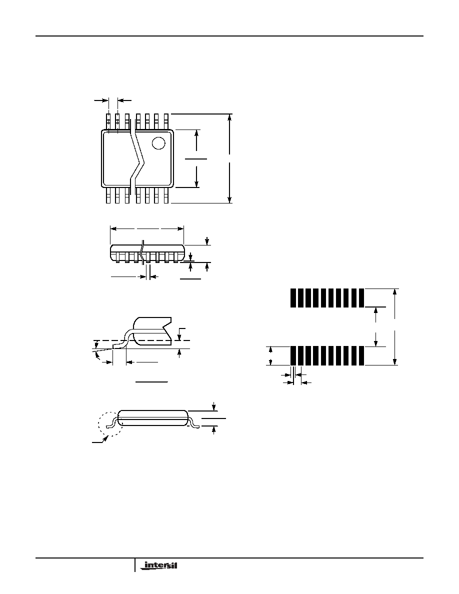
NOTE: ALL DIMENSIONS IN INCHES (IN PARENTHESES IN MILLIMETERS)
20-LEAD PLASTIC, TSSOP PACKAGE TYPE V
.169 (4.3)
.177 (4.5)
.252 (6.4) BSC
.025 (.65) BSC
.252 (6.4)
.260 (6.6)
.002 (.05)
.006 (.15)
.047 (1.20)
.0075 (.19)
.0118 (.30)
See Detail "A"
.031 (.80)
.041 (1.05)
0
∞
- 8
∞
.010 (.25)
.019 (.50)
.029 (.75)
Gage Plane
Seating Plane
Detail A (20X)
(4.16) (7.72)
(1.78)
(0.42)
(0.65)
ALL MEASUREMENTS ARE TYPICAL
X9523
30
All Intersil U.S. products are manufactured, assembled and tested utilizing ISO9000 quality systems.
Intersil Corporation's quality certifications can be viewed at www.intersil.com/design/quality
Intersil products are sold by description only. Intersil Corporation reserves the right to make changes in circuit design, software and/or specifications at any time without
notice. Accordingly, the reader is cautioned to verify that data sheets are current before placing orders. Information furnished by Intersil is believed to be accurate and
reliable. However, no responsibility is assumed by Intersil or its subsidiaries for its use; nor for any infringements of patents or other rights of third parties which may result
from its use. No license is granted by implication or otherwise under any patent or patent rights of Intersil or its subsidiaries.
For information regarding Intersil Corporation and its products, see www.intersil.com
FN8209.0
March 10, 2005
ORDERING INFORMATION
Device
Preset (Factory Shipped) V
TRIPx
Threshold Levels
(x = 1,2,3)
A = Optimized for 3.3V system monitoring
B = Optimized for 5V system monitoring
Temperature Range
I = Industrial -40
∞
C to +85
∞
C
Package
V20 = 20-Lead TSSOP
B20 = 20-Lead XBGA
X9523
P
T
XBGA PART MARK CONVENTION
20 Lead XBGA
Top Mark
X9523B20I-A
XACO
X9523B20I-B
XACS
-
y
For details of preset threshold values
,
See "D.C. OPERATING CHARACTERISTICS"
X9523