1
Æ
FN8215.1
CAUTION: These devices are sensitive to electrostatic discharge; follow proper IC Handling Procedures.
1-888-INTERSIL or 1-888-468-3774
|
Intersil (and design) is a registered trademark of Intersil Americas Inc.
Copyright Intersil Americas Inc. 2005. All Rights Reserved
All other trademarks mentioned are the property of their respective owners.
X96011
Temperature Sensor with Look Up Table Memory and DAC
FEATURES
∑ Single Programmable Current Generator
--±1.6 mA max.
--8-bit (256 Step) Resolution
--Internally Programmable full scale Current
Outputs
∑ Integrated 8-bit A/D Converter
∑ Internal Voltage Reference
∑ Temperature Compensation
--Internal Sensor
---40∞C to +100∞C Range
--2.2∞C / step resolution
--EEPROM Look-up Table
∑ Hot Pluggable
∑ Write Protection Circuitry
--Intersil BlockLockTM
--Logic Controlled Protection
∑ 2-wire Bus with 3 Slave Address Bits
∑ 3V to 5.5V, Single Supply Operation
∑ Package
--14 Ld TSSOP
∑ Pb-Free Plus Anneal Available (RoHS Compliant)
APPLICATIONS
∑ PIN Diode Bias Control
∑ RF PA Bias Control
∑ Temperature Compensated Process Control
∑ Laser Diode Bias Control
∑ Fan Control
∑ Motor Control
∑ Sensor Signal Conditioning
∑ Data Aquisition Applications
∑ Gain vs. Temperature Control
∑ High Power Audio
∑ Open Loop Temperature Compensation
∑ Close Loop Current, Voltage, Pressure, Temper-
ature, Speed, Position Programmable Voltage
sources, electronic loads, output amplifiers, or
function generator
DESCRIPTION
The X96011 is a highly integrated bias controller which
incorporates a digitally controlled Programmable Cur-
rent Generator, and temperature compensation using
one look-up table. All functions of the device are con-
trolled via a 2-wire digital serial interface.
The temperature compensated Programmable Current
Generator varies the output current with temperature
according to the contents of the associated nonvolatile
look-up table. The look-up table may be programmed
with arbitrary data by the user, via the 2-wire serial
port, and an internal temperature sensor is used to
control the output current response.
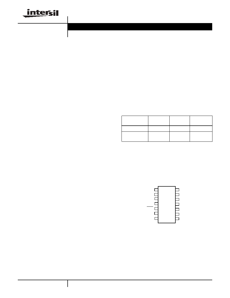
PIN CONFIGURATION
Ordering Information
PART NUMBER
PART
MARKING
TEMP
RANGE (∞C)
PACKAGE
X96011V14I
X96011V I
-40 to 100
14 Ld TSSOP
X96011V14IZ
(Note)
X96011VI Z
-40 to 100
14 Ld TSSOP
(Pb-free)
NOTE: Intersil Pb-free plus anneal products employ special Pb-free
material sets; molding compounds/die attach materials and 100% matte
tin plate termination finish, which are RoHS compliant and compatible
with both SnPb and Pb-free soldering operations. Intersil Pb-free
products are MSL classified at Pb-free peak reflow temperatures that
meet or exceed the Pb-free requirements of IPC/JEDEC J STD-020.
Vss
A2
3
4
NC
NC
NC
Vcc
A0
1
10
11
9
12
7
8
SCL
6
A1
2
WP
5
NC
NC
13
14
I
OUT
SDA
TSSOP 14L
Data Sheet
October 25, 2005
2
FN8215.1
October 25, 2005
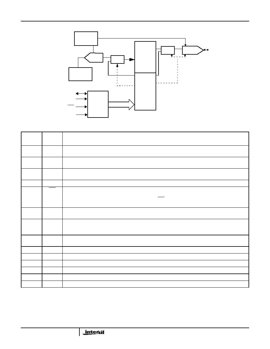
BLOCK DIAGRAM
PIN ASSIGNMENTS
TSSOP
Pin
Pin
Name
Pin Description
1
A0
Device Address Select Pin 0. This pin determines the LSB of the device address
required to communicate using the 2-wire interface. The A0 pin has an on-chip pull-down resistor.
2
A1
Device Address Select Pin 1. This pin determines the intermediate bit of the device address re-
quired to communicate using the 2-wire interface. The A1 pin has an on-chip pull-down resistor.
3
A2
Device Address Select Pin 2. This pin determines the MSB of the device address required to com-
municate using the 2-wire interface. The A2 pin has an on-chip pull-down resistor.
4
Vcc
Supply Voltage.
5
WP
Write Protect Control Pin. This pin is a CMOS compatible input. When LOW, Write Protection is
enabled preventing any "Write" operation. When HIGH, various areas of the memory can be pro-
tected using the Block Lock bits BL1 and BL0. The WP pin has an on-chip pull-down resistor, which
enables the Write Protection when this pin is left floating.
6
SCL
Serial Clock. This is a TTL compatible input pin. This input is the 2-wire interface clock controlling
data input and output at the SDA pin.
7
SDA
Serial Data. This pin is the 2-wire interface data into or out of the device. It is TTL
compatible when used as an input, and it is Open Drain when used as an output. This pin requires
an external pull up resistor.
8
I
OUT
Current Generator Output. This pin sinks or sources current. The magnitude and direction of the
current is fully programmable and adaptive. The resolution is 8 bits.
9
NC
No Connect.
10
NC
No Connect.
11
Vss
Ground.
12
NC
No Connect.
13
NC
No Connect.
14
NC
No Connect.
SDA
SCL
WP
2-Wire
I
OUT
Interface
A2, A1, A0
DAC
ADC
Look-up
Table
Control
& Status
Mux
Mux
Temperature
Sensor
Voltage
Reference
X96011

3
FN8215.1
October 25, 2005
ABSOLUTE MAXIMUM RATINGS
All voltages are referred to Vss.
Temperature under bias ................... -65∞C to +100∞C
Storage temperature ........................ -65∞C to +150∞C
Voltage on every pin except Vcc
................ -1.0V to +7V
Voltage on Vcc Pin .............................................0 to 5.5V
D.C. Output Current at pin SDA
...................... 0 to 5 mA
D.C. Output Current at pins Iout ....................... -3 to 3mA
Lead temperature (soldering, 10s) .................... 300∞C
COMMENT
Stresses above those listed under "Absolute Maximum
Ratings" may cause permanent damage to the device.
This is a stress rating only; functional operation of the
device (at these or any other conditions above those
listed in the operational sections of this specification) is
not implied. Exposure to absolute maximum rating con-
ditions for extended periods may affect device reliability.
RECOMMENDED OPERATING CONDITIONS
Parameter
Min.
Max.
Units
Temperature
-40
+100
∞C
Temperature while writing to memory
0
+70
∞C
Voltage on Vcc Pin
3
5.5
V
Voltage on any other Pin
-0.3
Vcc + 0.3
V
X96011
4
FN8215.1
October 25, 2005
ELECTRICAL CHARACTERISTICS (Conditions are as follows, unless otherwise specified)
All typical values are for 25∞C ambient temperature and 5 V at pin Vcc. Maximum and minimum specifications are over
the recommended operating conditions. All voltages are referred to the voltage at pin Vss. Bit 7 in control register 0 is
"1", while other bits in control registers are "0". 400kHz TTL input at SCL. SDA pulled to Vcc through an external 2k
resistor. 2-wire interface in "standby" (see notes 1 and 2 below). WP, A0, A1, and A2 floating.
Notes: 1. The device goes into Standby: 200 ns after any STOP, except those that initiate a nonvolatile write cycle. It goes into Standby t
WC
after
a STOP that initiates a nonvolatile write cycle. It also goes into Standby 9 clock cycles after any START that is not followed by the cor-
rect Slave Address Byte.
2. t
WC
is the time from a valid STOP condition at the end of a write sequence to the end of the self-timed internal nonvolatile write cycle. It
is the minimum cycle time to be allowed for any nonvolatile write by the user, unless Acknowledge Polling is used.
3. This parameter is periodically sampled and not 100% tested.
Symbol
Parameter
Min
Typ
Max
Unit
Test Conditions / Notes
Iccstby
Standby current into Vcc
pin
2
mA
Iout floating, sink mode
Iccfull
Full operation current into
Vcc pin
6
mA
2-wire interface reading from
memory, Iout connected to Vss,
DAC input bytes: FFh
Iccwrite
Nonvolatile Write current
into Vcc pin
4
mA
Average from START condition
until t
WP
after the STOP condition
WP: Vcc, Iout floating, sink mode
VRef unloaded.
I
PLDN
On-chip pull down current
at WP, A0, A1,and A2
0
1
20
µ
A
V(WP), V(A0), V(A1), and V(A2)
from 0V to Vcc
V
ILTTL
SCL and SDA, input Low
voltage
0.8 V
V
IHTTL
SCL and SDA, input High
voltage
2.0
V
I
INTTL
SCL and SDA input
current
-1
10
µ
A
Pin voltage between 0 and Vcc,
and SDA as an input.
V
OLSDA
SDA output Low voltage
0
0.4
V
I(SDA) = 2 mA
I
OHSDA
SDA output High current
0
100
µ
A
V(SDA) = Vcc
V
ILCMOS
WP, A0, A1, and A2 input
Low voltage
0
0.2 x Vcc
V
V
IHCMOS
WP, A0, A1, and A2 input
High voltage
0.8 x Vcc
Vcc
V
TSenseRange
Temperature sensor range
-40
100
∞C
See note 3.
V
POR
Power-on reset threshold
voltage
1.5
2.8
V
VccRamp
Vcc Ramp Rate
0.2
50
mV /
µ
s
V
ADCOK
ADC enable minimum
voltage
2.6
2.8
V
See Figure 8.
X96011
5
FN8215.1
October 25, 2005
D/A CONVERTER CHARACTERISTICS (See pg. 5 for standard conditions)
Notes: 1. LSB is defined as
divided by the resistance between R1 or R2 to Vss.
2. Offset
DAC
: The Offset of a DAC is defined as the deviation between the measured and ideal output, when the DAC input is 01h. It is
expressed in LSB.
FSError
DAC
: The Full Scale Error of a DAC is defined as the deviation between the measured and ideal output, when the input is FFh. It
is expressed in LSB. The Offset
DAC
is subtracted from the measured value before calculating FSError
DAC
.
DNL
DAC
: The Differential Non-Linearity of a DAC is defined as the deviation between the measured and ideal incremental change in
the output of the DAC, when the input changes by one code step. It is expressed in LSB. The measured values are adjusted for Offset
and Full Scale Error before calculating DNL
DAC
.
INL
DAC
: The Integral Non-Linearity of a DAC is defined as the deviation between the measured and ideal transfer curves, after adjust-
ing the measured transfer curve for Offset and Full Scale Error. It is expressed in LSB.
3. These parameters are periodically sampled and not 100% tested.
Symbol
Parameter
Min
Typ
Max
Unit
Test Conditions / Notes
IFS
Iout full scale current
1.56
1.58
1.6
mA
DAC input Byte = FFh,
Source or sink mode, V(Iout) is
Vcc≠1.2V in source mode and
1.2V in sink mode.
See notes 1 and 2.
Offset
DAC
Iout D/A converter offset error
1
1
LSB
FSError
DAC
Iout D/A converter full scale error
-2
2
LSB
DNL
DAC
Iout D/A converter
Differential Nonlinearity
-0.5
0.5
LSB
INL
DAC
Iout D/A converter Integral
Nonlinearity with respect to a
straight line through 0 and the full
scale value
-1
1
LSB
VISink
I1 Sink Voltage Compliance
1.2
Vcc
V
In this range the current at I1
vary < 1%
VISource
I1 Source Voltage Compliance
0
Vcc -
1.2
V
In this range the current at I1
vary < 1%
I
OVER
I1 overshoot on D/A Converter data
byte transition
0
µ
A
DAC input byte changing from
00h to FFh and vice
versa, V(I1) is Vcc - 1.2V in
source mode and 1.2V in sink
mode.
See note 3.
I
UNDER
I1 undershoot on D/A Converter
data byte transition
0
µ
A
t
rDAC
I1 rise time on D/A Converter data
byte transition; 10% to 90%
5
30
µ
s
TCO
I1I2
Temperature coefficient of output
current Iout
±200
ppm/∞C
See Figure 5.
2
3
V(VRef)
255
x
[
]
X96011
6
FN8215.1
October 25, 2005
A/D CONVERTER CHARACTERISTICS (See pg. 5 for standard conditions)
Notes: 1. "LSB" is defined as V(VRef)/255, "Full Scale" is defined as V(VRef).
2. Offset
ADC
: For an ideal converter, the first transition of its transfer curve occurs at
above zero. Offset error is the
amount of deviation between the measured first transition point and the ideal point.
FSError
ADC
: For an ideal converter, the last transition of its transfer curve occurs at
. Full Scale Error is the
amount of deviation between the measured last transition point and the ideal point,
after subtracting the Offset from the measured curve.
DNL
ADC
: DNL is defined as the difference between the ideal and the measured code transitions for successive A/D code outputs
expressed in LSBs. The measured transfer curve is adjusted for Offset and Fullscale errors before calculating DNL.
INL
ADC
: The deviation of the measured transfer function of an A/D converter from the ideal transfer function. The INL error is also
defined as the sum of the DNL errors starting from code 00h to the code where the INL measurement is desired. The measured trans-
fer curve is adjusted for Offset and Fullscale errors before calculating INL.
3. These parameters are periodically sampled and not 100% tested.
Symbol
Parameter
Min
Typ
Max
Unit
Test Conditions / Notes
ADCTIME
A/D converter conversion
time
9
ms
Proportional to A/D converter
input voltage. This value is
maximum at full scale input
of A/D converter.
ADCfiltOff = "1"
The ADC is monotonic
Offset
ADC
A/D converter offset error
±1
LSB
See notes 1 and 2
FSError
ADC
A/D converter full scale error
±1
LSB
DNL
ADC
A/D Converter Differential
Nonlinearity
±0.5
LSB
INL
ADC
A/D converter Integral
Nonlinearity
±1
LSB
TempStep
ADC
Temperature step causing
one step increment of ADC
output
0.52
0.55
0.58
∞C
See note 3
Out25
ADC
ADC output at 25∞C
01110101
2
0.5
x V(VRef)
255
[
]
254.5
x V(VRef)
255
[
]
X96011
7
FN8215.1
October 25, 2005
2-WIRE INTERFACE A.C. CHARACTERISTICS
2-WIRE INTERFACE TEST CONDITIONS
NONVOLATILE WRITE CYCLE TIMING
Notes: 1. Cb = total capacitance of one bus line (SDA or SCL) in pF.
2. t
WC
is the time from a valid STOP condition at the end of a write sequence to the end of the self-timed internal nonvolatile write cycle. It
is the minimum cycle time to be allowed for any nonvolatile write by the user, unless Acknowledge Polling is used.
3. The minimum frequency requirement applies between a START and a STOP condition.
4. These parameters are periodically sampled and not 100% tested.
Symbol
Parameter
Min
Typ
Max
Units
Test Conditions / Notes
f
SCL
SCL Clock Frequency
1
(3)
400
kHz
See "2-Wire Interface Test
Conditions" (below),
See Figure 1, Figure 2 and
Figure 3.
t
IN
(4)
Pulse width Suppression Time at
inputs
50
ns
t
AA
(4)
SCL Low to SDA Data Out Valid
900
ns
t
BUF
(4)
Time the bus free before start of new
transmission
1300
ns
t
LOW
Clock Low Time
1.3
1200
(3)
µ
s
t
HIGH
Clock High Time
0.6
1200
(3)
µ
s
t
SU:STA
Start Condition Setup Time
600
ns
t
HD:STA
Start Condition Hold Time
600
ns
t
SU:DAT
Data In Setup Time
100
ns
t
HD:DAT
Data In Hold Time
0
µ
s
t
SU:STO
Stop Condition Setup Time
600
ns
t
DH
Data Output Hold Time
50
ns
t
R
(4)
SDA and SCL Rise Time
20
+0.1Cb
(1)
300
ns
t
F
(4)
SDA and SCL Fall Time
20
+0.1Cb
(1)
300
ns
t
SU:WP
(4)
WP Setup Time
600
ns
t
HD:WP
(4)
WP Hold Time
600
ns
Cb
(4)
Capacitive load for each bus line
400
pF
Input Pulse Levels
10 % to 90 % of Vcc
Input Rise and Fall Times, between 10% and 90%
10 ns
Input and Output Timing Threshold Level
1.4V
External Load at pin SDA
2.3k
to Vcc and 100 pF to Vss
Symbol
Parameter
Min
Typ
Max
Units
Test Conditions / Notes
t
WC
(2)
Nonvolatile Write Cycle Time
5
10
ms
See Figure 3
X96011

8
FN8215.1
October 25, 2005
TIMING DIAGRAMS
Figure 1. Bus Timing
Figure 2. WP Pin Timing
Figure 3. Non-Volatile Write Cycle Timing
t
SU:STO
t
DH
t
HIGH
t
SU:STA
t
HD:STA
t
HD:DAT
t
SU:DAT
SCL
SDA IN
SDA OUT
t
F
t
LOW
t
BUF
t
AA
t
R
t
HD:WP
SCL
SDA IN
WP
t
SU:WP
Clk 1
START
STOP
SCL
SDA
t
WC
8th bit of last byte
ACK
Stop
Condition
Start Condition
X96011
9
FN8215.1
October 25, 2005
INTERSIL SENSOR CONDITIONER PRODUCT FAMILY
FSO = Full Scale Output, Ext = External, Int = Internal
DEVICE DESCRIPTION
The combination of the X96011 functionality and Inter-
sil's QFN package lowers system cost, increases reli-
ability, and reduces board space requirements.
The on-chip Programmable Current Generator may be
independently programmed to either sink or source
current. The maximum current generated is deter-
mined by using an externally connected programming
resistor, or by selecting one of three predefined val-
ues. Both current generators have a maximum output
of ±1.6 mA, and may be controlled to an absolute res-
olution of 0.39% (256 steps / 8 bit).
The current generator is driven using either an on-
board temperature sensor or Control Registers. The
internal temperature sensor operates over a very
broad temperature range (-40
∞
C
to +100
∞
C). The sen-
sor output drives an 8-bit A/D converter. The six MSBs
of the ADC output select one of 64 bytes from the non-
volatile look-up table (LUT).
The contents of the selected LUT row (8-bit wide)
drives the input of an 8-bit D/A converter, which gener-
ates the output current.
All control and setup parameters of the X96011,
including the look-up table, are programmable via the
2-wire serial port.
Device
Title
Features / Functions
Internal
Temperature
Sensor
External
Sensor
Input
Internal
Voltage
Reference
VREF
Input /
Ouput
General
Purpose
EEPROM
Look Up
Table
Organi-
zation
# of
DACs
FSO
Current
DAC
Setting
Resistors
X96010
Sensor Conditioner with
Dual Look-Up Table
Memory and DACs
No
Yes
Yes
Yes
No
Dual Bank
Dual
Ext
X96011
Temperature Sensor with
Look-Up Table Memory
and DAC
Yes
No
Yes
No
No
Single
Bank
Single
Int
X96012
Universal Sensor
Conditioner with Dual
Look-Up Table Memory
and DACs
Yes
Yes
Yes
Yes
Yes
Dual Bank
Dual
Ext / Int
X96011

10
FN8215.1
October 25, 2005
PRINCIPLES OF OPERATION
CONTROL AND STATUS REGISTERS
The Control and Status Registers provide the user
with a mechanism for changing and reading the value
of various parameters of the X96011. The X96011
contains five Control, one Status, and several
Reserved registers, each being one Byte wide (See
Figure 4). The Control registers 0 through 6 are
located at memory addresses 80h through 86h
respectively. The Status register is at memory address
87h, and the Reserved registers at memory address
82h, 84h, and 88h through 8Fh.
All bits in Control register 6 always power-up to the logic
state "0". All bits in Control registers 0 through 5 power-
up to the logic state value kept in their corresponding
nonvolatile memory cells. The nonvolatile bits of a reg-
ister retain their stored values even when the X96011 is
powered down, then powered back up. The nonvolatile
bits in Control 0 through Control 5 registers are all pre-
programmed to the logic state "0" at the factory, except
the cases that indicate "1" in Figure 1.
Bits indicated as "Reserved" are ignored when read,
and must be written as "0", if any Write operation is
performed to their registers.
A detailed description of the function of each of the
Control and Status register bits follows:
Control Register 0
This register is accessed by performing a Read or
Write operation to address 80h of memory.
ADC
FILT
O
FF
: ADC F
ILTERING
C
ONTROL
(N
ON
-
VOLATILE
)
When this bit is "1", the status register at 87h is
updated after every conversion of the ADC. When this
bit is "0" (default), the status register is updated after
four consecutive conversions with the same result, on
the 6 MSBs.
NV13: C
ONTROL
REGISTERS
1
AND
3
VOLATILITY
MODE
SELECTION
BIT
(N
ON
-
VOLATILE
)
When the NV13 bit is set to "0" (default), bytes written
to Control registers 1 and 3 are stored in volatile cells,
and their content is lost when the X96011 is powered
down. When the NV13 bit is set to "1", bytes written to
Control registers 1 and 3 are stored in both volatile
and nonvolatile cells, and their value doesn't change
when the X96011 is powered down and powered back
up. See "Writing to Control Registers" on page 21.
IDS: C
URRENT
G
ENERATOR
D
IRECTION
S
ELECT
B
IT
(N
ON
-
VOLATILE
)
The IDS bit sets the polarity of the Current Generator.
When this bit is set to "0" (default), the Current Gener-
ator of the X96011 is configured as a Current Source.
The Current Generator is configured as a Current Sink
when the IDS bit is set to "1". See Figure 5.
X96011
11
FN8215.1
October 25, 2005
Figure 4. Control and Status Register Format
Byte
MSB
LSB
80h
Register
Control 0
0
0
IDS
NV13
1
ADCfiltOff
0
0
Non-Volatile
81h
Control 1
Volatile or
Reserved Reserved
LDA5
LDA4
LDA3
LDA2
LDA1
LDA0
83h
Control 3
Volatile or
DDA7
DDA6
DDA5
DDA4
DDA3
DDA2
DDA1
DDA0
Non-Volatile
Non-Volatile
85h
Control 5
Non-Volatile
0
0
DDAS
LDAS
0
0
IFSO1
IFSO0
86h
Control 6
Volatile
WEL
Reserved Reserved Reserved Reserved
Reserved Reserved
Reserved
87h
Status
Volatile
AD7
AD6
AD5
AD4
AD3
AD2
AD1
AD0
7
6
5
4
3
2
1
0
Name
Address
Registers in byte addresses 82h, 84h, and 88h through 8Fh are reserved.
Direct Access to the LUT
Direct Access to the DAC
ADC Output
Iout
0: Source
1: Sink
Control
1, 3
Volatility
0: Volatile
1: Non-
volatile
Direct
Direct
Access
to DAC
Access
to LUT
0: Disabled 0: Disabled
1: Enabled 1: Enabled
R Selection
00: Reserved
01: Low Internal
10: Middle Internal
11: High Internal (Default)
Write
Enable
Latch
0: Write
Disabled
1: Write
Enabled
ADC
0: On
1: Off
filtering
Direction
Registers bits shown as 0 or 1 should always use these values for proper operation.
X96011
12
FN8215.1
October 25, 2005
Control Register 1
This register is accessed by performing a Read or Write
operation to address 81h of memory. This byte's volatility
is determined by bit NV13 in Control register 0.
LDA5 - LDA0: LUT D
IRECT
A
CCESS
B
ITS
When bit LDAS (bit 4 in Control register 5) is set to "1",
the LUT is addressed by these six bits, and it is not
addressed by the output of the on-chip A/D converter.
When bit LDAS is set to "0", these six bits are ignored
by the X96011. See Figure 7.
A value between 00h (00
10
) and 3Fh (63
10
) may be writ-
ten to these register bits, to select the corresponding row
in the LUT. The written value is added to the base
address of the LUT (90h).
Control Register 3
This register is accessed by performing a Read or Write
operation to address 83h of memory. This byte's volatility
is determined by bit NV13 in Control register 0.
DDA7 - DDA0: D/A D
IRECT
A
CCESS
B
ITS
When bit DDAS (bit 5 in Control register 5) is set to "1",
the input to the D/A converter is the content of bits
DDA7 - DDA0, and it is not a row of LUT. When bit
DDAS is set to "0" (default) these eight bits are ignored
by the X96011. See Figure 6.
Control Register 5
This register is accessed by performing a Read or
Write operation to address 85h of memory.
IFSO1 - IFSO0: C
URRENT
G
ENERATOR
F
ULL
S
CALE
O
UTPUT
S
ET
B
ITS
(N
ON
-
VOLATILE
)
These two bits are used to set the full scale output cur-
rent at the Current Generator pin, Iout, according to
the following table. The direction of this current is set
by bit IDS in Control register 0. See Figure 5.
LDAS: LUT D
IRECT
A
CCESS
S
ELECT
B
IT
(N
ON
-
VOLATILE
)
When bit LDAS is set to "0" (default), the LUT is
addressed by the output of the on-chip A/D converter.
When bit LDAS is set to "1", LUT is addressed by bits
LDA5 - LDA0.
DDAS: D/A D
IRECT
A
CCESS
S
ELECT
B
IT
(N
ON
-
VOLATILE
)
When bit DDAS is set to "0" (default), the input to
the D/A converter is a row of the LUT. When bit
DDAS is set to "1", that input is the content of the
Control register 3.
Control Register 6
This register is accessed by performing a Read or
Write operation to address 86h of memory.
I1FSO1 I1FSO0
I1 Full Scale Output Current
0
0
Reserved (Don't Use)
0
1
±
0.4mA
1
0
±
0.85 mA
1
1
±
1.3 mA (Default)
X96011

13
FN8215.1
October 25, 2005
WEL: W
RITE
E
NABLE
L
ATCH
(V
OLATILE
)
The WEL bit controls the Write Enable status of the
entire X96011 device. This bit must be set to "1" before
any other Write operation (volatile or nonvolatile). Oth-
erwise, any proceeding Write operation to memory is
aborted and no ACK is issued after a Data Byte.
The WEL bit is a volatile latch that powers up in the "0"
state (disabled). The WEL bit is enabled by writing
10000000
2
to Control register 6. Once enabled, the
WEL bit remains set to "1" until the X96011 is powered
down, and then up again, or until it is reset to "0" by
writing 00000000
2
to Control register 6.
A Write operation that modifies the value of the WEL bit
will not cause a change in other bits of Control register 6.
Status Register - ADC Output
This register is accessed by performing a Read opera-
tion to address 87h of memory.
AD7 - AD0: A/D C
ONVERTER
O
UTPUT
B
ITS
(R
EAD
ONLY
)
This byte is the binary output of the on-chip digital
thermometer. The output is 00000000
2
for -40∞C and
11111111
2
for 100∞C. The six MSBs select a row of
the LUT.
LOOK-UP TABLE
The X96011 memory array contains a 64-byte look-up
table. The look-up table is associated to pin Iout's out-
put current generator through the D/A converter. The
output of the look-up table is the byte contained in the
selected row. By default this byte is the input to the
D/A converter driving pin Iout.
The byte address of the selected row is obtained by
adding the look-up table base address 90h, and the
appropriate row selection bits. See Figure 6.
By default the look-up table selection bits are the
6 MSBs of the digital thermometer output. Alter-
natively, the A/D converter can be bypassed and the
six row selection bits are the six LSBs of Control
Register 1 for the LUT. The selection between these
options is illustrated in Figure 6.
CURRENT GENERATOR BLOCK
The Current Generator pin Iout is the output of the cur-
rent mode D/A converter.
D/A Converter Operation
The Block Diagram for the D/A converter is shown in
Figure 5.
The input byte of the D/A converter selects a voltage
on the non-inverting input of an operational amplifier.
The output of the amplifier drives the gate of a FET.
This node is also fed back to the inverting input of the
amplifier. The drain of the FET is connected to the out-
put current pin (Iout) via a "polarity select" circuit block.
X96011
14
FN8215.1
October 25, 2005
Figure 5. D/A Converter Block Diagram
+
-
Iout Pin
IDS: bit
Vss
Vss
IFSO[1:0]
Low_Cur
re
nt
Midd
le
_Cur
re
nt
Hi
gh_
Cur
r
en
t
Internal
Select
Circuit
Polarity
Vcc
Voltage
6 in Control
register 0.
Divider
DAC
Input byte
Vss
bits 1 and 0
in Control
register 5
11
10 01
Reference
Voltage
Figure 6. Look-up Table (LUT) Operation
DAC
8
90h
90h
CFh
8
LUT
6
LUT Row
Out
D1
D0
Select
DDAS: Bit 5 of
DDA[7:0] : Control register 3
Selection bits
A
D
D
E
R
8
8
Input Byte
Control register 5
...
X96011
15
FN8215.1
October 25, 2005
By examining the block diagram in Figure 5, we see
that the maximum current through pin Iout is set by fix-
ing values for V(VRef) and R. The output current can
then be varied by changing the data byte at the D/A
converter input.
In general, the magnitude of the current at the D/A
converter output pin may be calculated by:
I = (V(VRef) / (384 ∑ R)) ∑ N
where N is the decimal representation of the input byte
to the corresponding D/A converter.
The value for the resistor determines the full scale out-
put current that the D/A converter may sink or source.
Bits IFSO1 and IFSO0 select the full scale output cur-
rent setting for Iout as described in "IFSO1 - IFSO0:
Current Generator Full Scale Output Set Bits (Non-vol-
atile)" on page 12.
Bit IDS and in Control Register 0 select the direction of
the currents through pins Iout (See "IDS: Current Gen-
erator Direction Select Bit (Non-volatile)" on page 10
and "Control and Status Register Format" on
page 11).
D/A Converter Output Current Response
When the D/A converter input data byte changes by
an arbitrary number of bits, the output current changes
from an intial current level (I
x
) to some final level
(I
x
+
I
x
). The transition is monotonic and glitchless.
D/A Converter Control
The data byte inputs of the D/A converters can be con-
trolled in three ways:
≠ 1) With the A/D converter and through the look-up
tables (default),
≠ 2) Bypassing the A/D converter and directly access-
ing the look-up tables,
≠ 3) Bypassing both the A/D converter and look-up
tables, and directly setting the D/A converter input
byte.
D1
D0
Select
ADC
AD[7:0]
LUT Row
Voltage
Voltage Input
Selection bits
Reference
Out
LDA[5:0]:
Control
Register 1
LDAS: bit 4 in
Control register 5
6
6
Status
Register
Figure 7. Look-Up Table Addressing
8
from Internal
temperature
sensor
X96011

16
FN8215.1
October 25, 2005
The options are summarized in the following tables:
D/A Converter Access Summary
Bit DDAS is used to bypass the A/D converter and
look-up table, allowing direct access to the input of the
D/A converter with the byte in control register 3. See
Figure 6, and the descriptions of the control bits.
Bit IDS in Control Register 0 select the direction of the
current through pin Iout. See Figure 5, and the
descriptions of the control bits.
POWER-ON RESET
When power is applied to the Vcc pin of the X96011, the
device undergoes a strict sequence of events before the
current outputs of the D/A converters are enabled.
When the voltage at Vcc becomes larger than the
power-on reset threshold voltage (V
POR
), the device
recalls all control bits from non-volatile memory into
volatile registers. Next, the analog circuits are pow-
ered up. When the voltage at Vcc becomes larger than
a second voltage threshold (V
ADCOK
), the ADC is
enabled. In the default case, after the ADC performs
four consecutive conversions with the same exact
result, the ADC output is used to select a byte from the
look-up table. The byte becomes the input of the DAC.
During all the previous sequence the input of the DAC
is 00h. If bit ADCfiltOff is "1", only one ADC conversion
is necessary. Bit DDAS and LDAS, also modify the
way the DAC is accessed the first time after power-up,
as described in "Control Register 5" on page 12.
The X96011 is a hot pluggable device. Voltage dis-
trubances on the Vcc pin are handled by the power-on
reset circuit, allowing proper operation during hot plug-
in applications.
LDAS
DDAS
Control Source
0
0
A/D converter through LUT
(Default)
1
0
Bits LDA5 - LDA0 through LUT
X
1
Bits DDA7 - DDA0
"X" = Don't Care Condition (May be either "1" or "0")
Figure 8. D/A Converter Power-on Reset Response
I
x
I
x
x 10%
ADC TIME
Current
Time
Time
Vcc
V
ADCOK
0V
Voltage
X96011

17
FN8215.1
October 25, 2005
SERIAL INTERFACE
Serial Interface Conventions
The device supports a bidirectional bus oriented proto-
col. The protocol defines any device that sends data
onto the bus as a transmitter, and the receiving device
as the receiver. The device controlling the transfer is
called the master and the device being controlled is
called the slave. The master always initiates data
transfers, and provides the clock for both transmit and
receive operations. The X96011 operates as a slave in
all applications.
Serial Clock and Data
Data states on the SDA line can change only while
SCL is LOW. SDA state changes while SCL is HIGH
are reserved for indicating START and STOP condi-
tions. See Figure 10. On power-up of the X96011, the
SDA pin is in the input mode.
Serial Start Condition
All commands are preceded by the START condition,
which is a HIGH to LOW transition of SDA while SCL
is HIGH. The device continuously monitors the SDA
and SCL lines for the START condition and does not
respond to any command until this condition has been
met. See Figure 9.
Serial Stop Condition
All communications must be terminated by a STOP
condition, which is a LOW to HIGH transition of SDA
while SCL is HIGH. The STOP condition is also used
to place the device into the Standby power mode after
a read sequence. A STOP condition can only be
issued after the transmitting device has released the
bus. See Figure 9.
Serial Acknowledge
An ACK (Acknowledge), is a software convention used
to indicate a successful data transfer. The transmitting
device, either master or slave, releases the bus after
transmitting eight bits. During the ninth clock cycle, the
receiver pulls the SDA line LOW to acknowledge the
reception of the eight bits of data. See Figure 11.
The device responds with an ACK after recognition of
a START condition followed by a valid Slave Address
byte. A valid Slave Address byte must contain the
Device Type Identifier 1010, and the Device Address
bits matching the logic state of pins A2, A1, and A0.
See Figure 13.
If a write operation is selected, the device responds
with an ACK after the receipt of each subsequent
eight-bit word.
In the read mode, the device transmits eight bits of
data, releases the SDA line, and then monitors the line
for an ACK. The device continues transmitting data if
an ACK is detected. The device terminates further
data transmissions if an ACK is not detected. The
master must then issue a STOP condition to place the
device into a known state.
The X96011 acknowledges all incoming data and
address bytes except: 1) The "Slave Address Byte"
when the "Device Identifier" or "Device Address" are
wrong; 2) All "Data Bytes" when the "WEL" bit is "0",
with the exception of a "Data Byte" addresses to loca-
tion 86h; 3) "Data Bytes" following a "Data Byte"
addressed to locations 80h, 85h, or 86h.
X96011
18
FN8215.1
October 25, 2005
Figure 9. Valid Start and Stop Conditions
Figure 10. Valid Data Changes on the SDA Bus
Figure 11. Acknowledge Response From Receiver
SCL
SDA
START
STOP
SCL
SDA
Data Stable
Data Change
Data Stable
SDA Output from
Transmitter
SDA Output from
Receiver
8
1
9
START
ACK
SCL from
Master
X96011
19
FN8215.1
October 25, 2005
X96011 Memory Map
The X96011 contains a 80 byte array of mixed volatile
and nonvolatile memory. This array is split up into two
distinct parts, namely: (Refer to figure 12.)
≠ Look-up Table (LUT)
≠ Control and Status Registers
Figure 12. X96011 Memory Map
The Control and Status registers of the X96011 are
used in the test and setup of the device in a system.
These registers are realized as a combination of both
volatile and nonvolatile memory. These registers
reside in the memory locations 80h through 8Fh. The
reserved bits within registers 80h through 86h, must
be written as "0" if writing to them, and should be
ignored when reading. Register bits shown as 0 or 1,
in Figure 4, must be written with the indicated value if
writing to them. The reserved registers, 82h, 84h, and
from 88h through 8Fh, must not be written, and their
content should be ignored.
The LUT is realized as nonvolatile EEPROM, and
extend from memory locations 90h≠CFh. This LUT is
dedicated to storing data solely for the purpose of set-
ting the outputs of Current Generators I
OUT
.
All bits in the LUT are preprogrammed to "0" at the
factory.
Addressing Protocol Overview
All Serial Interface operations must begin with a
START, followed by a Slave Address Byte. The Slave
address selects the X96011, and specifies if a Read or
Write operation is to be performed.
It should be noted that the Write Enable Latch (WEL)
bit must first be set in order to perform a Write opera-
tion to any other bit. (See "WEL: Write Enable Latch
(Volatile)" on page 13.) Also, all communication to the
X96011 over the 2-wire serial bus is conducted by
sending the MSB of each byte of data first.
The memory is physically realized as one contiguous
array, organized as 5 pages of 16 bytes each.
The X96011 2-wire protocol provides one address
byte. The next few sections explain how to access the
different areas for reading and writing.
Figure 13. Slave Address (SA) Format
Address
Size
64 Bytes
16 Bytes
80h
8Fh
90h
CFh
Look-up Table
(LUT)
Control & Status
Registers
SA6
SA7
SA5
SA3 SA2
SA1
SA0
Device Type
Identifier
Read or
SA4
Slave Address
Bit(s)
Description
SA7 - SA4
Device Type Identifier
SA3 - SA1
Device Address
SA0
Read or Write Operation Select
R/W
1
0
1
0
Address
Device
AS0
AS1
AS2
Write
X96011
20
FN8215.1
October 25, 2005
Slave Address Byte
Following a START condition, the master must output
a Slave Address Byte (Refer to figure 13.). This byte
includes three parts:
≠ The four MSBs (SA7 - SA4) are the Device Type
Identifier, which must always be set to 1010 in order
to select the X96011.
≠ The next three bits (SA3 - SA1) are the Device
Address bits (AS2 - AS0). To access any part of the
X96011's memory, the value of bits AS2, AS1, and
AS0 must correspond to the logic levels at pins A2,
A1, and A0 respectively.
≠ The LSB (SA0) is the R/W bit. This bit defines the
operation to be performed on the device being
addressed. When the R/W bit is "1", then a Read
operation is selected. A "0" selects a Write
operation (Refer to figure 13.)
Nonvolatile Write Acknowledge Polling
After a nonvolatile write command sequence is cor-
rectly issued (including the final STOP condition), the
X96011 initiates an internal high voltage write cycle.
This cycle typically requires 5 ms. During this time,
any Read or Write command is ignored by the
X96011. Write Acknowledge Polling is used to deter-
mine whether a high voltage write cycle is completed.
During acknowledge polling, the master first issues a
START condition followed by a Slave Address Byte.
The Slave Address Byte contains the X96011's Device
Type Identifier and Device Address. The LSB of the
Slave Address (R/W) can be set to either 1 or 0 in this
case. If the device is busy within the high voltage
cycle, then no ACK is returned. If the high voltage
cycle is completed, an ACK is returned and the master
can then proceed with a new Read or Write operation.
(Refer to figure 14.).
Byte Write Operation
In order to perform a Byte Write operation to the mem-
ory array, the Write Enable Latch (WEL) bit of the Con-
trol 6 Register must first be set to "1". (See "WEL:
Write Enable Latch (Volatile)" on page 13.)
For any Byte Write operation, the X96011 requires the
Slave Address Byte, an Address Byte, and a Data Byte
(See Figure 15). After each of them, the X96011
responds with an ACK. The master then terminates the
transfer by generating a STOP condition. At this time, if
all data bits are volatile, the X96011 is ready for the next
read or write operation. If some bits are nonvolatile, the
X96011 begins the internal write cycle to the nonvolatile
memory. During the internal nonvolatile write cycle, the
X96011 does not respond to any requests from the
master. The SDA output is at high impedance.
Writing to Control bytes which are located at byte
addresses 80h through 8Fh is a special case
described in the section "Writing to Control Registers" .
Page Write Operation
The 80-byte memory array is physically realized as
one contiguous array, organized as 5 pages of 16
bytes each. A "Page Write" operation can be per-
formed to any of the four LUT pages. In order to per-
form a Page Write operation, the Write Enable Latch
(WEL) bit in Control register 6 must first be set (See
"WEL: Write Enable Latch (Volatile)" on page 13.)
A Page Write operation is initiated in the same manner
as the byte write operation; but instead of terminating
the write cycle after the first data byte is transferred,
the master can transmit up to 16 bytes (See Figure
16). After the receipt of each byte, the X96011
responds with an ACK, and the internal byte address
counter is incremented by one. The page address
remains constant. When the counter reaches the end
of the page, it "rolls over" and goes back to the first
byte of the same page.
ACK returned?
Issue Slave Address
Byte (Read or Write)
Byte load completed by issuing
STOP. Enter ACK Polling
Issue STOP
Issue START
NO
YES
NO
Continue normal Read or Write
command sequence
PROCEED
YES
complete. Continue command
sequence.
High Voltage
Issue STOP
Figure 14. Acknowledge Polling Sequence
X96011
21
FN8215.1
October 25, 2005
For example, if the master writes 12 bytes to a 16-byte
page starting at location 11 (decimal), the first 5 bytes
are written to locations 11 through 15, while the last 7
bytes are written to locations 0 through 6 within that
page. Afterwards, the address counter would point to
location 7. If the master supplies more than 16 bytes of
data, then new data overwrites the previous data, one
byte at a time (See Figure 17).
The master terminates the loading of Data Bytes by
issuing a STOP condition, which initiates the nonvola-
tile write cycle. As with the Byte Write operation, all
inputs are disabled until completion of the internal
write cycle.
A Page Write operation cannot be performed on the
page at locations 80h through 8Fh. Next section
describes the special cases within that page.
Writing to Control Registers
The bytes at locations 80h, 81h, 83h, 85h, and 86h are
written using Byte Write operations. They cannot be
written using a Page Write operation.
Registers Control 1 and 3 have a nonvolatile and a vol-
atile cell for each bit. At power-up, the content of the
nonvolatile cells is automatically recalled and written to
the volatile cells. The content of the volatile cells con-
trols the X96011's functionality. If bit NV13 in the Con-
trol 0 register is set to "1", a Write operation to these
registers writes to both the volatile and nonvolatile cells.
If bit NV13 in the Control 0 register is set to "0", a Write
operation to these registers only writes to the volatile
cells. In both cases the newly written values effectively
control the X96011, but in the second case, those val-
ues are lost when the part is powered down.
If bit NV13 is set to "0", a Byte Write operation to Con-
trol registers 0 or 5 causes the value in the nonvolatile
cells of Control registers 1 and 3 to be recalled into
their corresponding volatile cells, as during power-up.
This doesn't happen when the WP pin is LOW,
because Write Protection is enabled. It is generally
recommended to configure Control registers 0 and 5
before writing to Control registers 1 or 3.
A "Byte Write" operation to Control register 1 or 3,
causes the value in the nonvolatile cells of the other to
be recalled into the corresponding volatile cells, as
during power-up.
When reading either of the control registers 1 or 3, the
Data Bytes are always the content of the correspond-
ing nonvolatile cells, even if bit NV13 is "0" (See "Con-
trol and Status Register Format").
S
t
a
r
t
S
t
o
p
Slave
Address
Address
Byte
Data
Byte
A
C
K
Signals from
the Master
Signals from
the Slave
A
C
K
1
0
1
0 0
A
C
K
Write
Signal at SDA
Figure 15. Byte Write Sequence
2 < n < 16
Signals from
the Master
Signals from
the Slave
Signal at SDA
S
t
a
r
t
Slave
Address
Address
Byte
A
C
K
A
C
K
1
0
1
0 0
Data Byte (1)
S
t
o
p
A
C
K
A
C
K
Data Byte (n)
Write
Figure 16. Page Write Operation
X96011
22
FN8215.1
October 25, 2005
Read Operation
A Read operation consist of a three byte instruction
followed by one or more Data Bytes (See Figure 18).
The master initiates the operation issuing the following
sequence: a START, the Slave Address byte with the
R/W bit set to "0", an Address Byte, a second START,
and a second Slave Address byte with the R/W bit set
to "1". After each of the three bytes, the X96011
responds with an ACK. Then the X96011 transmits
Data Bytes as long as the master responds with an
ACK during the SCL cycle following the eigth bit of
each byte. The master terminates the read operation
(issuing a STOP condition) following the last bit of the
last Data Byte (See Figure 18).
The Data Bytes are from the memory location indicated
by an internal pointer. This pointer initial value is deter-
mined by the Address Byte in the Read operation instruc-
tion, and increments by one during transmission of each
Data Byte. After reaching the memory location CFh a
stop should be issued. If the read operation continues the
output bytes are unpredictable. If the byte address is set
between 00h and 7Fh, or higher than CFh, the output
bytes are unpredictable.
A Read operation internal pointer can start at any
memory location from 80h through CFh, when the
Address Byte is 80h through CFh respectively.
When reading any of the control registers 1, 2, 3, or 4,
the Data Bytes are always the content of the corre-
sponding nonvolatile cells, even if bit NV13 is "0" (See
"Control and Status Register Format").
Data Protection
There are three levels of data protection designed into
the X96011: 1- Any Write to the device first requires
setting of the WEL bit in Control 6 register; 2- The
Write Protection pin disables any writing to the
X96011; 3- The proper clock count, data bit sequence,
and STOP condition is required in order to start a nonvol-
atile write cycle, otherwise the X96011 ignores the Write
operation.
WP: Write Protection Pin
When the Write Protection (WP) pin is active (LOW),
any Write operations to the X96011 is disabled, except
the writing of the WEL bit.
5 bytes
7 bytes
Address = 6
5 bytes
Address Pointer
Address = 15
Address = 11
Ends Up Here
Address = 7
Address = 0
Figure 17. Example: Writing 12 bytes to a 16-byte page starting at location 11.
Signals
from the
Master
Signals from
the Slave
Signal at
SDA
S
t
a
r
t
Slave
Address
with
R/W = 0
Address
Byte
A
C
K
A
C
K
1
0
1
0 0
S
t
o
p
A
C
K
1
1
1
0 0
Slave
Address
with
R/W = 1
A
C
K
S
t
a
r
t
Last Read
Data Byte
First Read
Data Byte
A
C
K
Figure 18. Read Sequence
X96011
23
All Intersil U.S. products are manufactured, assembled and tested utilizing ISO9000 quality systems.
Intersil Corporation's quality certifications can be viewed at www.intersil.com/design/quality
Intersil products are sold by description only. Intersil Corporation reserves the right to make changes in circuit design, software and/or specifications at any time without
notice. Accordingly, the reader is cautioned to verify that data sheets are current before placing orders. Information furnished by Intersil is believed to be accurate and
reliable. However, no responsibility is assumed by Intersil or its subsidiaries for its use; nor for any infringements of patents or other rights of third parties which may result
from its use. No license is granted by implication or otherwise under any patent or patent rights of Intersil or its subsidiaries.
For information regarding Intersil Corporation and its products, see www.intersil.com
FN8215.1
October 25, 2005
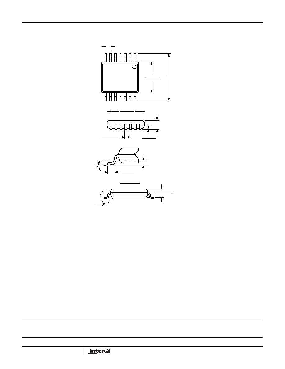
PACKAGING INFORMATION
NOTE: ALL DIMENSIONS IN INCHES (IN PARENTHESES IN MILLIMETERS)
14-Lead Plastic, TSSOP, Package Code V14
See Detail "A"
.031 (.80)
.041 (1.05)
.169 (4.3)
.177 (4.5) .252 (6.4) BSC
.025 (.65) BSC
.193 (4.9)
.200 (5.1)
.002 (.05)
.006 (.15)
.041 (1.05)
.0075 (.19)
.0118 (.30)
0∞ - 8∞
.010 (.25)
.019 (.50)
.029 (.75)
Gage Plane
Seating Plane
Detail A (20X)
X96011