 | –≠–ª–µ–∫—Ç—Ä–æ–Ω–Ω—ã–π –∫–æ–º–ø–æ–Ω–µ–Ω—Ç: X9C503SI | –°–∫–∞—á–∞—Ç—å:  PDF PDF  ZIP ZIP |
1
Æ
FN8222.1
CAUTION: These devices are sensitive to electrostatic discharge; follow proper IC Handling Procedures.
1-888-INTERSIL or 1-888-468-3774
|
Intersil (and design) is a registered trademark of Intersil Americas Inc.
XDCP is a trademark of Intersil Americas Inc. Copyright Intersil Americas Inc. 2005. All Rights Reserved
All other trademarks mentioned are the property of their respective owners.
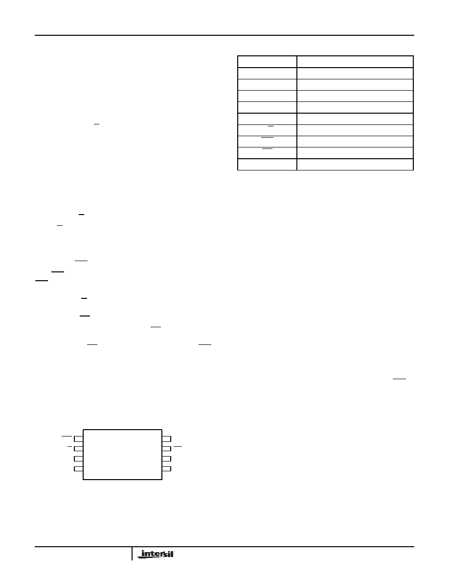
X9C102, X9C103, X9C104, X9C503
Digitally Controlled Potentiometer
(XDCPTM)
FEATURES
∑ Solid-state potentiometer
∑ 3-wire serial interface
∑ 100 wiper tap points
--Wiper position stored in nonvolatile memory
and recalled on power-up
∑ 99 resistive elements
--Temperature compensated
--End to end resistance, ±20%
--Terminal voltages, ±5V
∑ Low power CMOS
--V
CC
= 5V
--Active current, 3mA max.
--Standby current, 750µA max.
∑ High reliability
--Endurance, 100,000 data changes per bit
--Register data retention, 100 years
∑ X9C102 = 1k
∑ X9C103 = 10k
∑ X9C503 = 50k
∑ X9C104 = 100k
∑ Packages
--8-lead SOIC and DIP
∑ Pb-free plus anneal available (RoHS compliant)
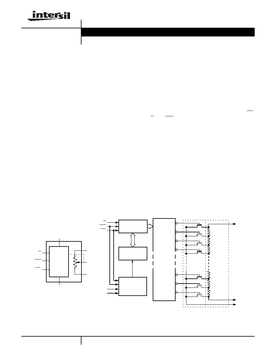
DESCRIPTION
The X9Cxxx are Intersil digitally controlled (XDCP)
potentiometers. The device consists of a resistor
array, wiper switches, a control section, and nonvola-
tile memory. The wiper position is controlled by a
three-wire interface.
The potentiometer is implemented by a resistor array
composed of 99 resistive elements and a wiper switch-
ing network. Between each element and at either end
are tap points accessible to the wiper terminal. The
position of the wiper element is controlled by the CS,
U/D, and INC inputs. The position of the wiper can be
stored in nonvolatile memory and then be recalled
upon a subsequent power-up operation.
The device can be used as a three-terminal potentiom-
eter or as a two-terminal variable resistor in a wide
variety of applications including:
≠ control
≠ parameter adjustments
≠ signal processing
BLOCK DIAGRAM
Up/Down
(INC)
Increment
Device
(U/D)
(CS)
V
CC
(Supply Voltage)
V
SS
(Ground)
7-Bit
Up/Down
Counter
7-Bit
Nonvolatile
Memory
Store and
Recall
Control
Circuitry
One
of
Hundred
Decoder
Resistor
Array
U/D
INC
CS
Transfer
V
CC
GND
One-
Gates
99
98
97
96
2
1
0
Control
and
Memory
General
Detailed
R
L
/V
L
R
W
/V
W
R
H
/V
H
V
H
/R
H
R
W
/V
W
V
L
/R
L
Select
Data Sheet
September 19, 2005

2
FN8222.1
September 19, 2005
PIN CONFIGURATION
V
CC
CS
V
L
/R
L
V
W
/R
W
INC
U/D
V
SS
1
2
3
4
8
7
6
5
V
H
/R
H
X9C102/103/104/503
DIP/SOIC
ORDERING INFORMATION
PART NUMBER
PART MARKING
R
TOTAL
(k
)
TEMPERATURE RANGE (∞C)
PACKAGE
X9C102P
X9C102P
1
0 to 70
8 Ld PDIP
X9C102PZ (Note)
X9C102P Z
0 to 70
8 Ld PDIP (Pb-free)
X9C102PI
X9C102P I
-40 to 85
8 Ld PDIP
X9C102PIZ (Note)
X9C102P Z I
-40 to 85
8 Ld PDIP (Pb-free)
X9C102S*
X9C102S
0 to 70
8 Ld SOIC
X9C102SZ* (Note)
X9C102S Z
0 to 70
8 Ld SOIC (Pb-free)
X9C102SI*
X9C102S I
-40 to 85
8 Ld SOIC
X9C102SIZ* (Note)
X9C102S Z I
-40 to 85
8 Ld SOIC (Pb-free)
X9C103P
X9C103P
10
0 to 70
8 Ld PDIP
X9C103PZ (Note)
X9C103P Z
0 to 70
8 Ld PDIP (Pb-free)
X9C103PI
X9C103P I
-40 to 85
8 Ld PDIP
X9C103PIZ (Note)
X9C103P Z I
-40 to 85
8 Ld PDIP (Pb-free)
X9C103S*
X9C103S
0 to 70
8 Ld SOIC
X9C103SZ* (Note)
X9C103S Z
0 to 70
8 Ld SOIC (Pb-free)
X9C103SI*
X9C103S I
-40 to 85
8 Ld SOIC
X9C103SIZ* (Note)
X9C103S Z I
-40 to 85
8 Ld SOIC (Pb-free)
X9C503P
X9C503P
50
0 to 70
8 Ld PDIP
X9C503PZ (Note)
X9C503P Z
0 to 70
8 Ld PDIP (Pb-free)
X9C503PI
X9C503P I
-40 to 85
8 Ld PDIP
X9C503PIZ (Note)
X9C503P Z I
-40 to 85
8 Ld PDIP (Pb-free)
X9C503S*
X9C503S
0 to 70
8 Ld SOIC
X9C503SZ* (Note)
X9C503S Z
0 to 70
8 Ld SOIC (Pb-free)
X9C503SI*
X9C503S I
-40 to 85
8 Ld SOIC
X9C503SIZ* (Note)
X9C503S Z I
-40 to 85
8 Ld SOIC (Pb-free)
X9C104P
X9C104P
100
0 to 70
8 Ld PDIP
X9C104P-3
0 to 70
8 Ld PDIP
X9C104PI
X9C104P I
-40 to 85
8 Ld PDIP
X9C104PIZ (Note)
X9C104P Z I
-40 to 85
8 Ld PDIP (Pb-free)
X9C104S*
X9C104S
0 to 70
8 Ld SOIC
X9C104SZ* (Note)
X9C104S Z
0 to 70
8 Ld SOIC (Pb-free)
X9C104SI*
X9C104S I
-40 to 85
8 Ld SOIC
X9C104SI-Z
-40 to 85
8 Ld SOIC
X9C104SIZ* (Note)
-40 to 85
8 Ld SOIC (Pb-free)
NOTE: Intersil Pb-free plus anneal products employ special Pb-free material sets; molding compounds/die attach materials and 100% matte tin plate
termination finish, which are RoHS compliant and compatible with both SnPb and Pb-free soldering operations. Intersil Pb-free products are MSL
classified at Pb-free peak reflow temperatures that meet or exceed the Pb-free requirements of IPC/JEDEC J STD-020.
*Add "T1" suffix for tape and reel.
X9C102, X9C103, X9C104, X9C503
3
FN8222.1
September 19, 2005
PIN DESCRIPTIONS
Pin
Symbol
Brief Description
1
INC
Increment . The
INC
input is negative-edge triggered. Toggling INC will move the wiper and either
increment or decrement the counter in the direction indicated by the logic level on the U/D input.
2
U/D
Up/Down. The U/D input controls the direction of the wiper movement and whether the counter
is incremented or decremented.
3
R
H
/V
H
R
H
/V
H
.
The high (V
H
/R
H
) terminals of the X9C102/103/104/503 are equivalent to the fixed
terminals of a mechanical potentiometer. The minimum voltage is -5V and the maximum is +5V.
The terminology of V
H
/R
H
and V
L
/R
L
references the relative position of the terminal in
relation to wiper movement direction selected by the U/D input and not the voltage potential on
the terminal.
4
V
SS
V
SS
5
V
W
/R
W
V
W
/R
W
.
V
W
/R
W
is the wiper terminal, and is equivalent to the movable terminal of a mechanical
potentiometer. The position of the wiper within the array is determined by the control inputs. The
wiper terminal series resistance is typically 40
.
6
R
L
/V
L
R
L
/V
L
.
The low (V
L
/R
L
) terminals of the X9C102/103/104/503 are equivalent to the fixed
terminals of a mechanical potentiometer. The minimum voltage is -5V and the maximum is +5V.
The terminology of V
H
/R
H
and V
L
/R
L
references the relative position of the terminal in
relation to wiper movement direction selected by the U/D input and not the voltage potential on
the terminal.
7
CS
CS. The device is selected when the CS input is LOW. The current counter value is stored in
nonvolatile memory when CS is returned HIGH while the INC input is also HIGH. After the store op-
eration is complete the X9C102/103/104/503 device will be placed in the low power standby mode
until the device is selected once again.
8
V
CC
V
CC
X9C102, X9C103, X9C104, X9C503

4
FN8222.1
September 19, 2005
ABSOLUTE MAXIMUM RATINGS
Temperature under bias .................... -65∞C to +135∞C
Storage temperature ......................... -65∞C to +150∞C
Voltage on CS, INC, U/D and V
CC
with respect to V
SS
.................................. -1V to +7V
Voltage on V
H
/R
H
and V
L
/R
L
referenced to V
SS
................................... -8V to +8V
V = |V
H
/R
H
- V
L
/R
L
|
X9C102 ...............................................................4V
X9C103, X9C503, and X9C104 ......................... 10V
Lead temperature (soldering, 10 seconds)...... +300∞C
I
W
(10 seconds) ................................................. 8.8mA
COMMENT
Stresses above those listed under "Absolute Maximum
Ratings" may cause permanent damage to the device.
This is a stress rating only; functional operation of the
device (at these or any other conditions above those
listed in the operational sections of this specification) is
not implied. Exposure to absolute maximum rating
conditions for extended periods may affect device reliability.
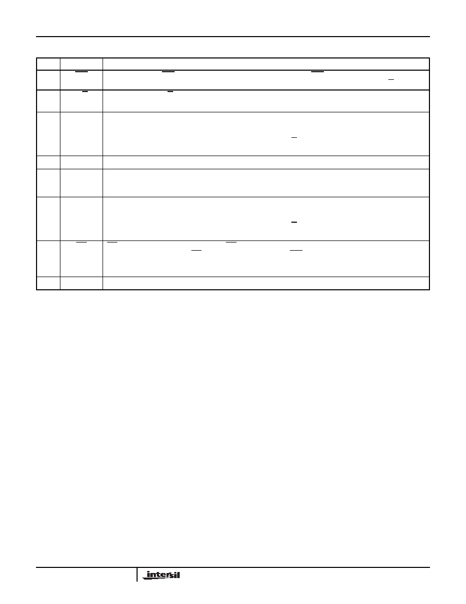
POTENTIOMETER CHARACTERISTICS (Over recommended operating conditions unless otherwise stated.)
Notes: (1) Absolute linearity is utilized to determine actual wiper voltage versus expected voltage = [V
W(n)(actual)
- V
W(n)(expected )
] = ±1 MI Maximum.
(2) Relative linearity is a measure of the error in step size between taps = V
W(n + 1)
- [V
W(n) + MI
] = +0.2 MI.
(3) 1 MI = Minimum Increment = R
TOT
/99
(4) Typical values are for T
A
= 25∞C and nominal supply voltage.
(5) This parameter is not 100% tested.
Symbol
Parameter
Limits
Unit
Test Conditions/Notes
Min.
Typ.
Max.
R
TOTAL
End to end resistance variation
-20
+20
%
V
VH/RH
V
H
terminal voltage
-5
+5
V
V
VL/RL
V
L
terminal voltage
-5
+5
V
Power rating
16
mW
X9C102
Power rating
10
mW
X9C103/104/503
I
W
Wiper current
-4.4
4.4
mA
R
W
Wiper resistance
40
100
Wiper Current = ±1mA
Noise
-120
dBV
Ref. 1kHz
Resolution
1
%
Absolute linearity
(1)
-1
+1
M
(3)
V
W(n)(actual)
- V
W(n)(expected)
Relative linearity
(2)
-0.2
+0.2
MI
(3)
V
W(n + 1)(actual)
- [V
W(n) + MI
]
RTOTAL temperature coefficient
±300
ppm/∞C X9C103/503/104
RTOTAL temperature coefficient
±600
ppm/∞C X9C102
Ratiometric temperature coefficient
±20
ppm/∞C
C
H
/C
L
/C
W
Potentiometer capacitances
10/10/25
pF
See Circuit #3, Macro Model
RECOMMENDED OPERATING CONDITIONS
Temperature
Min.
Max.
Commercial
0∞C
+70∞C
Industrial
-40∞C
+85∞C
Supply Voltage (V
CC
)
Limits
X9C102/103/104/503
5V ±10%
X9C102, X9C103, X9C104, X9C503
5
FN8222.1
September 19, 2005
D.C. OPERATING CHARACTERISTICS (Over recommended operating conditions unless otherwise specified.)
ENDURANCE AND DATA RETENTION
A.C. CONDITIONS OF TEST
Symbol
Parameter
Limits
Unit
Test Conditions
Min. Typ.
(4)
Max.
I
CC
V
CC
active current
1
3
mA
CS = V
IL
, U/D = V
IL
or V
IH
and
INC = 0.4V to 2.4V @ max. t
CYC
I
SB
Standby supply current
200
750
µA
CS = V
CC
- 0.3V, U/D and INC = V
SS
or V
CC
- 0.3V
I
LI
CS, INC, U/D input leakage
current
±10
µA
V
IN
= V
SS
to V
CC
V
IH
CS, INC, U/D input HIGH
voltage
2
V
CC
+ 1
V
V
IL
CS, INC, U/D input LOW
voltage
-1
0.8
V
C
IN
(2)
CS, INC, U/D input
capacitance
10
pF
V
CC
= 5V, V
IN
= V
SS
, T
A
= 25∞C, f = 1MHz
Parameter
Min.
Unit
Minimum endurance
100,000
Data changes per bit per register
Data retention
100
years
Input pulse levels
0V to 3V
Input rise and fall times
10ns
Input reference levels
1.5V
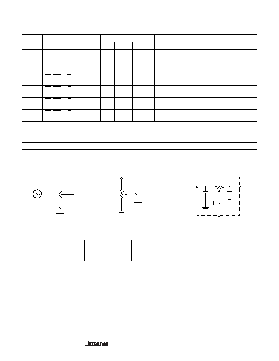
Test Circuit #1
Test Circuit #2
Test Circuit #3
Test Point
V
W
/R
W
VR/RH
V
S
V
L
/R
L
Force
Current
V
H
/R
H
Test Point
V
W
/R
W
V
L
/R
L
R
H
C
H
10pF
C
W
R
L
C
L
R
W
R
TOTAL
25pF
10pF
Macro Model
X9C102, X9C103, X9C104, X9C503
6
FN8222.1
September 19, 2005
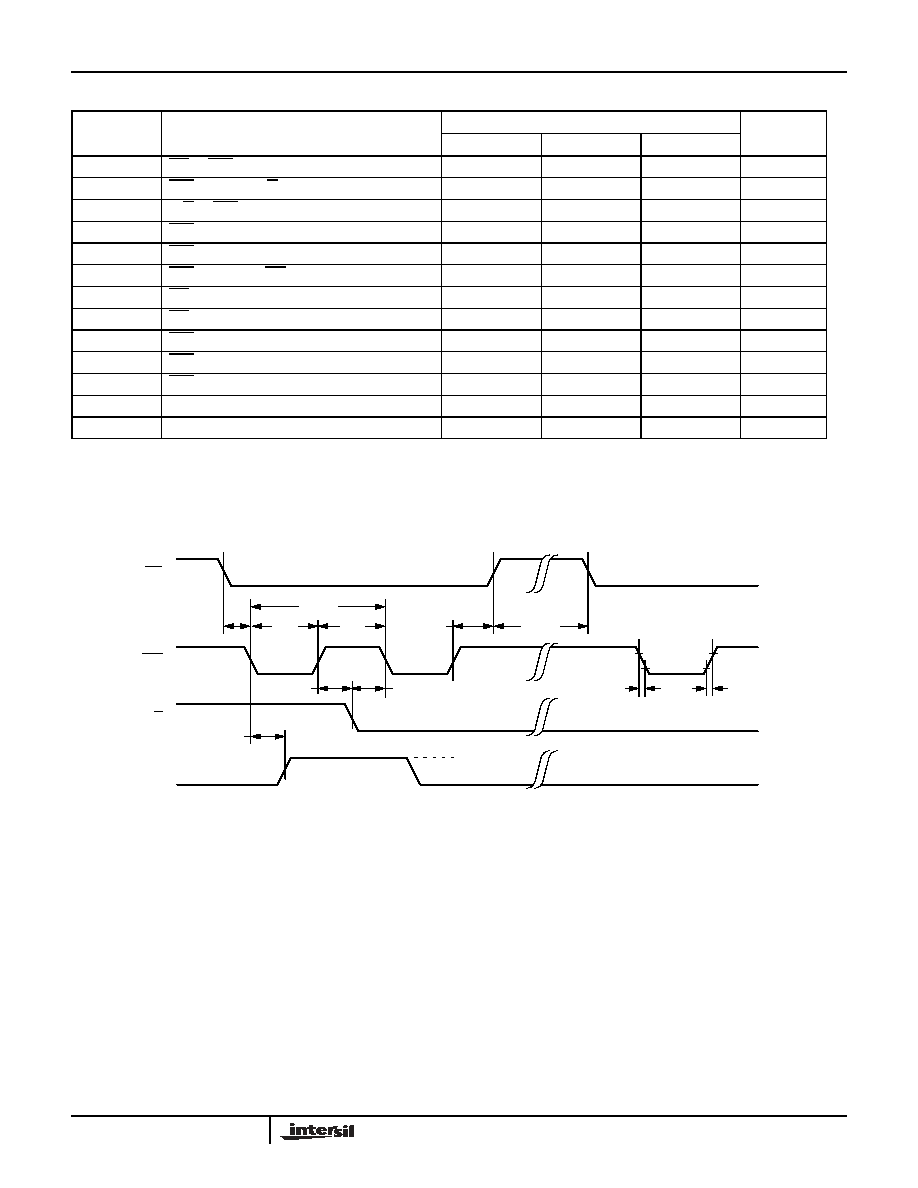
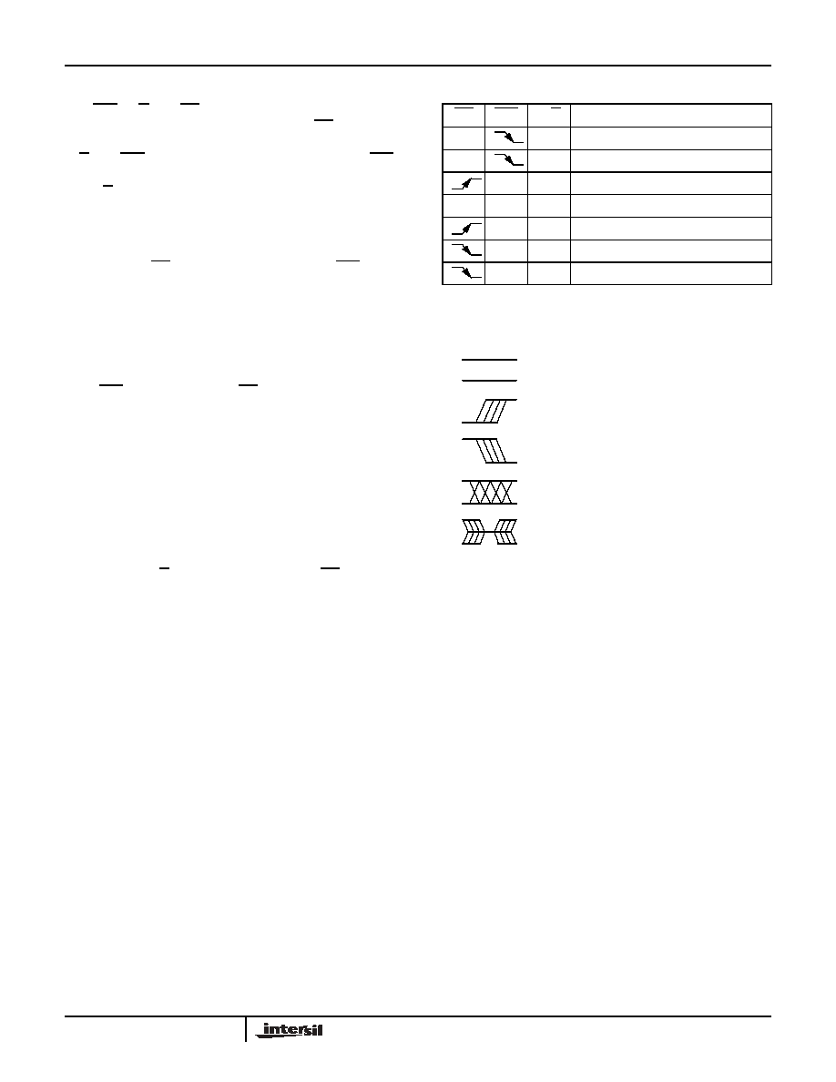
A.C. OPERATING CHARACTERISTICS (Over recommended operating conditions unless otherwise specified)
POWER-UP AND DOWN REQUIREMENTS
At all times, voltages on the potentiometer pins must be less than ±V
CC
. The recall of the wiper position from nonvola-
tile memory is not in effect until the V
CC
supply reaches its final value. The V
CC
ramp rate spec is always in effect.
A.C. TIMING
Notes: (6) Typical values are for TA = 25∞C and nominal supply voltage.
(7) This parameter is periodically sampled and not 100% tested.
(8) MI in the A.C. timing diagram refers to the minimum incremental change in the V
W
output due to a change in the wiper position.
Symbol
Parameter
Limits
Unit
Min.
Typ.
(6)
Max.
t
Cl
CS to INC setup
100
ns
t
lD
INC HIGH to U/D change
100
ns
t
DI
U/D to INC setup
2.9
µs
t
lL
INC LOW period
1
µs
t
lH
INC HIGH period
1
µs
t
lC
INC inactive to CS inactive
1
µs
t
CPH
CS deselect time (STORE)
20
ms
t
CPH
CS deselect time (NO STORE)
100
ns
t
IW
INC to V
W/RW
change
100
500
µs
t
CYC
INC cycle time
4
µs
t
R,
t
F
(7)
INC input rise and fall time
500
µs
t
PU
(7)
Power-up to wiper stable
500
µs
t
R
V
CC
(7)
V
CC
power-up rate
0.2
50
V/ms
CS
INC
U/D
V
W
t
CI
t
IL
t
IH
t
CYC
t
ID
t
DI
t
IW
MI
(8)
t
IC
t
CPH
t
F
t
R
10%
90%
90%
X9C102, X9C103, X9C104, X9C503
7
FN8222.1
September 19, 2005
DETAILED PIN DESCRIPTIONS
R
H
/V
H
and R
L
/V
L
The high (V
H
/R
H
) and low (V
L
/R
L
) terminals of the
X9C102/103/104/503 are equivalent to the fixed termi-
nals of a mechanical potentiometer. The minimum
voltage is -5V and the maximum is +5V. The terminol-
ogy of V
H
/R
H
and V
L
/R
L
references the relative position
of the terminal in relation to wiper movement direction
selected by the U/D input and not the voltage potential
on the terminal.
R
W
/V
W
V
W
/R
W
is the wiper terminal, and is equivalent to the
movable terminal of a mechanical potentiometer. The
position of the wiper within the array is determined by
the control inputs. The wiper terminal series resistance is
typically 40
.
Up/Down (U/D)
The U/D input controls the direction of the wiper move-
ment and whether the counter is incremented or dec-
remented.
Increment (INC)
The
INC
input is negative-edge triggered. Toggling
INC will move the wiper and either increment or decre-
ment the counter in the direction indicated by the logic
level on the U/D input.
Chip Select (CS)
The device is selected when the CS input is LOW.
The current counter value is stored in nonvolatile
memory when CS is returned HIGH while the INC
input is also HIGH. After the store operation is com-
plete the X9C102/103/104/503 device will be placed
in the low power standby mode until the device is
selected once again.
PIN CONFIGURATION
PIN NAMES
PRINCIPLES OF OPERATION
There are three sections of the X9Cxxx: the input con-
trol, counter and decode section; the nonvolatile mem-
ory; and the resistor array. The input control section
operates just like an up/down counter. The output of
this counter is decoded to turn on a single electronic
switch connecting a point on the resistor array to the
wiper output. Under the proper conditions the contents
of the counter can be stored in nonvolatile memory
and retained for future use. The resistor array is com-
prised of 99 individual resistors connected in series. At
either end of the array and between each resistor is an
electronic switch that transfers the potential at that
point to the wiper.
The wiper, when at either fixed terminal, acts like its
mechanical equivalent and does not move beyond the
last position. That is, the counter does not wrap
around when clocked to either extreme.
The electronic switches on the device operate in a
"make before break" mode when the wiper changes
tap positions. If the wiper is moved several positions,
multiple taps are connected to the wiper for t
IW
(INC to
V
W
/R
W
change). The R
TOTAL
value for the device can
temporarily be reduced by a significant amount if the
wiper is moved several positions.
When the device is powered-down, the last wiper posi-
tion stored will be maintained in the nonvolatile mem-
ory. When power is restored, the contents of the
memory are recalled and the wiper is set to the value
last stored.
V
CC
CS
V
L
/R
L
V
W
/R
W
INC
U/D
V
SS
1
2
3
4
8
7
6
5
V
H
/R
H
X9C102/103/104/503
DIP/SOIC
Symbol
Description
V
H
/R
H
High Terminal
V
W
/R
W
Wiper Terminal
V
L
/R
L
Low Terminal
V
SS
Ground
V
CC
Supply Voltage
U/D
Up/Down Control Input
INC
Increment Control Input
CS
Chip Select Control Input
NC
No Connection
X9C102, X9C103, X9C104, X9C503
8
FN8222.1
September 19, 2005
INSTRUCTIONS AND PROGRAMMING
The INC, U/D and CS inputs control the movement of
the wiper along the resistor array. With CS set LOW
the device is selected and enabled to respond to the
U/D and INC inputs. HIGH to LOW transitions on INC
will increment or decrement (depending on the state of
the U/D input) a seven-bit counter. The output of this
counter is decoded to select one of one-hundred wiper
positions along the resistive array.
The value of the counter is stored in nonvolatile mem-
ory whenever CS transitions HIGH while the INC input
is also HIGH.
The system may select the X9Cxxx, move the wiper,
and deselect the device without having to store the lat-
est wiper position in nonvolatile memory. After the
wiper movement is performed as described above and
once the new position is reached, the system must
keep INC LOW while taking CS HIGH. The new wiper
position will be maintained until changed by the sys-
tem or until a power-down/up cycle recalled the previ-
ously stored data.
This procedure allows the system to always power-up
to a preset value stored in nonvolatile memory; then
during system operation minor adjustments could be
made. The adjustments might be based on user pref-
erence: system parameter changes due to tempera-
ture drift, etc...
The state of U/D may be changed while CS remains
LOW. This allows the host system to enable the
device and then move the wiper up and down until the
proper trim is attained.
MODE SELECTION
SYMBOL TABLE
CS
INC
U/D
Mode
L
H
Wiper Up
L
L
Wiper Down
H
X
Store Wiper Position
H
X
X
Standby Current
L
X
No Store, Return to Standby
L
H
Wiper Up (not recommended)
L
L
Wiper Down (not recommended)
WAVEFORM
INPUTS
OUTPUTS
Must be
steady
Will be
steady
May change
from Low to
High
Will change
from Low to
High
May change
from High to
Low
Will change
from High to
Low
Don't Care:
Changes
Allowed
Changing:
State Not
Known
N/A
Center Line
is High
Impedance
X9C102, X9C103, X9C104, X9C503

9
FN8222.1
September 19, 2005
PERFORMANCE CHARACTERISTICS
Contact the factory for more information.
APPLICATIONS INFORMATION
Electronic digitally controlled (XCDP) potentiometers provide three powerful application advantages; (1) the variability
and reliability of a solid-state potentiometer, (2) the flexibility of computer-based digital controls, and (3) the retentivity
of nonvolatile memory used for the storage of multiple potentiometer settings or data.
Basic Configurations of Electronic Potentiometers
Basic Circuits
V
R
V
R
I
Three terminal potentiometer;
variable voltage divider
Two terminal variable resistor;
variable current
V
H
/R
H
V
L
/R
L
V
W
/R
W
Cascading Techniques
Buffered Reference Voltage
≠
+
+5V
R
1
+V
-5V
V
W
V
REF
V
OUT
OP-07
V
W
/R
W
V
W
/R
W
+V
+V
+V
X
(a)
(b)
V
OUT
= V
W
/R
W
Noninverting Amplifier
V
O
= (1+R
2
/R
1
)V
S
Voltage Regulator
R
1
R
2
I
adj
V
O
(REG) = 1.25V (1+R
2
/R
1
)+I
adj
R
2
V
O
(REG)
V
IN
317
Offset Voltage Adjustment
+
≠
V
S
V
O
R
2
R
1
100k
10k
10k
10k
-12V
+12V
TL072
Comparator with Hysteresis
V
UL
= {R
1
/(R
1
+ R
2
)} V
O
(max)
V
LL
= {R
1
/(R
1
+ R
2
)} V
O
(min)
+
≠
V
S
V
O
R
2
R
1
LM308A
+5V
-5V
+
≠
V
S
V
O
R
2
R
1
}
}
LT311A
(for additional circuits see AN115)
X9C102, X9C103, X9C104, X9C503
10
FN8222.1
September 19, 2005
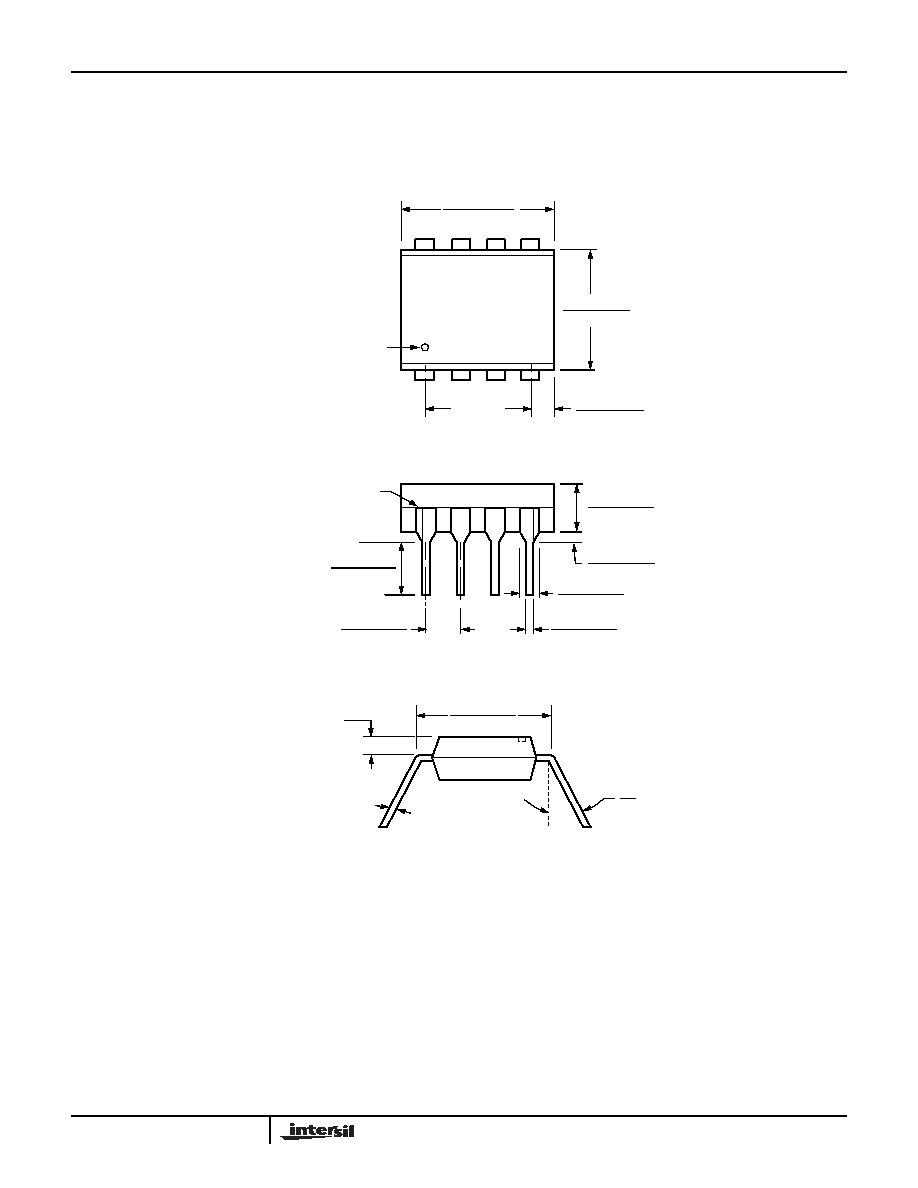
PACKAGING INFORMATION
NOTE:
1. ALL DIMENSIONS IN INCHES (IN PARENTHESES IN MILLIMETERS)
2. PACKAGE DIMENSIONS EXCLUDE MOLDING FLASH
0.020 (0.51)
0.016 (0.41)
0.150 (3.81)
0.125 (3.18)
0.110 (2.79)
0.090 (2.29)
0.430 (10.92)
0.360 (9.14)
0.300
(7.62) Ref.
Pin 1 Index
0.145 (3.68)
0.128 (3.25)
0.025 (0.64)
0.015 (0.38)
Pin 1
Seating
0.065 (1.65)
0.045 (1.14)
0.260 (6.60)
0.240 (6.10)
0.060 (1.52)
0.020 (0.51)
Typ. 0.010 (0.25)
0∞
15∞
8-Lead Plastic Dual In-Line Package Type P
Half Shoulder Width On
All End Pins Optional
.073 (1.84)
Max.
0.325 (8.25)
0.300 (7.62)
Plane
X9C102, X9C103, X9C104, X9C503
11
All Intersil U.S. products are manufactured, assembled and tested utilizing ISO9000 quality systems.
Intersil Corporation's quality certifications can be viewed at www.intersil.com/design/quality
Intersil products are sold by description only. Intersil Corporation reserves the right to make changes in circuit design, software and/or specifications at any time without
notice. Accordingly, the reader is cautioned to verify that data sheets are current before placing orders. Information furnished by Intersil is believed to be accurate and
reliable. However, no responsibility is assumed by Intersil or its subsidiaries for its use; nor for any infringements of patents or other rights of third parties which may result
from its use. No license is granted by implication or otherwise under any patent or patent rights of Intersil or its subsidiaries.
For information regarding Intersil Corporation and its products, see www.intersil.com
FN8222.1
September 19, 2005
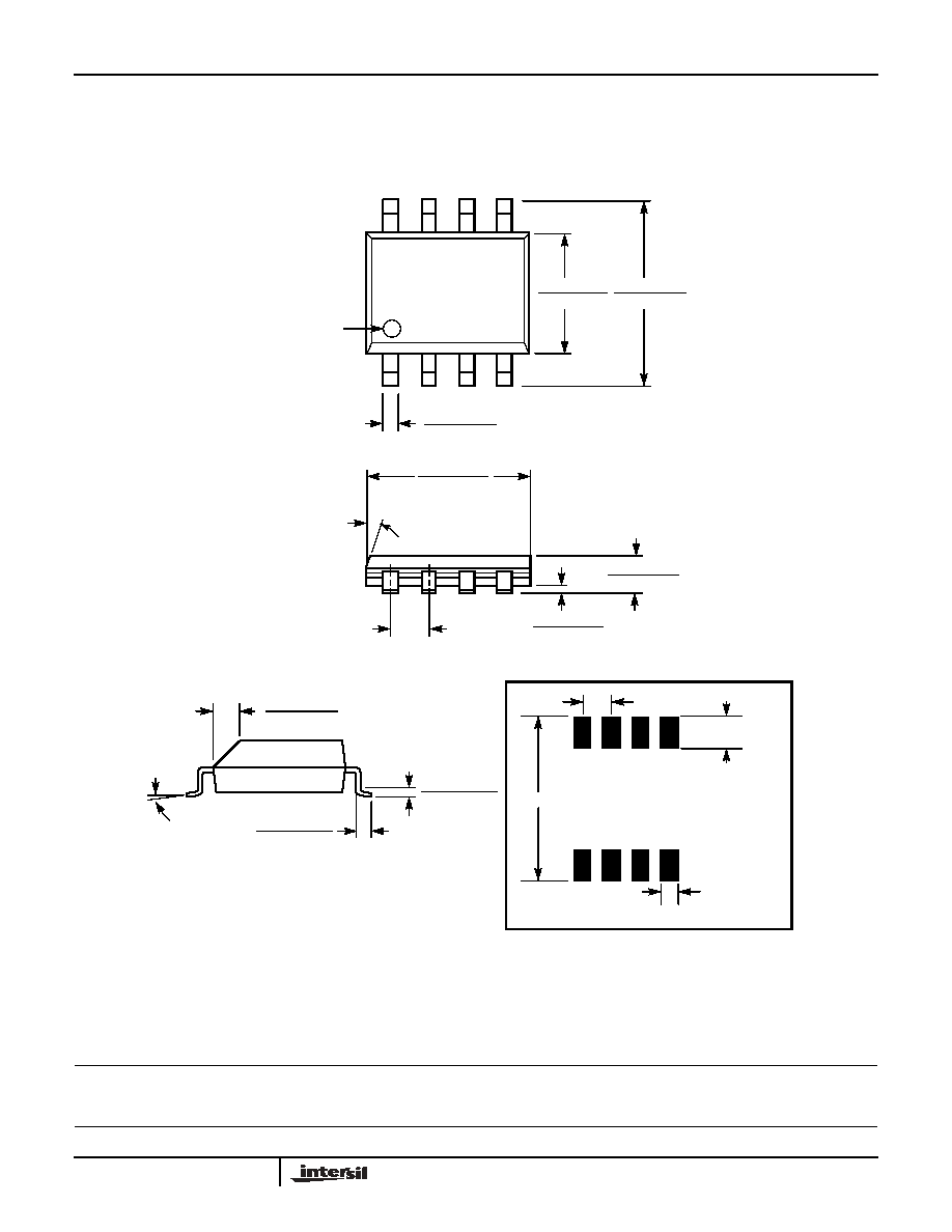
PACKAGING INFORMATION
0.150 (3.80)
0.158 (4.00)
0.228 (5.80)
0.244 (6.20)
0.014 (0.35)
0.019 (0.49)
Pin 1
Pin 1 Index
0.010 (0.25)
0.020 (0.50)
0.050 (1.27)
0.188 (4.78)
0.197 (5.00)
0.004 (0.19)
0.010 (0.25)
0.053 (1.35)
0.069 (1.75)
(4X) 7∞
0.016 (0.410)
0.037 (0.937)
0.0075 (0.19)
0.010 (0.25)
0∞ - 8∞
X 45∞
8-Lead Plastic Small Outline Gull Wing Package Type S
NOTE: ALL DIMENSIONS IN INCHES (IN PARENTHESES IN MILLIMETERS)
0.250"
0.050" Typical
0.050"
Typical
0.030"
Typical
8 Places
FOOTPRINT
X9C102, X9C103, X9C104, X9C503