Model
Input Voltage
Range (Vin)
I in No
Load
I in Full
Load
Vo
(V)
Io
(A)
Eff
Typ (%)
Case
Pinout
Regulation
Line/Load (%)
Riple/Noise
Typ. (mVp-p)
Q150-48S1.5
36 - 75
0.100
1.80
1.5
45
85
Q150
QS
�0.2 / �0.2
100
Q150-48S1.8
36 - 75
0.100
2.20
1.8
45
86
Q150
QS
�0.1 / �0.1
100
Q150-48S2.5
36 - 75
0.100
2.80
2.5
40
87
Q150
QS
�0.1 / �0.1
100
Q150-48S3.3
36 - 75
0.100
3.20
3.3
35
89
Q150
QS
�0.1 / �0.1
100
Q150-48S5
36 - 75
0.100
4.00
5
30
91
Q150
QS
�0.1 / �0.1
100
Q150-48S12
36 - 75
0.100
4.10
12
12
93
Q150
QS
�0.1 / �0.1
100
H75-12S2.5
9 - 18
0.050
4.11
2.5
15.0
76
H
HS
�0.2 / �0.2
75
H75-12S3.3
9 - 18
0.050
5.29
3.3
15.0
78
H
HS
�0.2 / �0.2
75
H75-12S5
9 - 18
0.050
7.72
5
15.0
81
H
HS
�0.2 / �0.2
75
H75-12S12
9 - 18
0.050
7.44
12
6.3
84
H
HS
�0.2 / �0.2
100
H75-12S15
9 - 18
0.050
7.44
15
5.0
84
H
HS
�0.2 / �0.2
100
H75-12S24
9 - 18
0.050
7.44
24
3.1
84
H
HS
�0.2 / �0.2
240
H100-24S2.5
18 - 36
0.050
2.71
2.5
20.0
77
H
HS
�0.2 / �0.2
50
H100-24S3.3
18 - 36
0.050
3.48
3.3
20.0
79
H
HS
�0.2 / �0.2
50
H100-24S5
18 - 36
0.050
5.02
5
20.0
83
H
HS
�0.2 / �0.2
50
H100-24S12
18 - 36
0.050
4.88
12
8.3
85
H
HS
�0.2 / �0.2
100
H100-24S15
18 - 36
0.050
4.93
15
6.7
85
H
HS
�0.2 / �0.2
100
H100-24S24
18 - 36
0.050
4.91
24
4.2
85
H
HS
�0.2 / �0.2
100
H120-48S1.5
36 - 75
0.100
1.10
1.5
30.0
85
H120
HS
�1.0 / �1.0
100
H120-48S1.8
36 - 75
0.100
1.30
1.8
30.0
86
H120
HS
�1.0 / �1.0
100
H120-48S2.5
36 - 75
0.100
1.80
2.5
30.0
87
H120
HS
�1.0 / �1.0
100
H120-48S3.3
36 - 75
0.100
3.10
3.3
40.0
87
H120
HS
�1.0 / �1.0
100
H120-48S5
36 - 75
0.100
2.30
5
20.0
90
H120
HS
�1.0 / �1.0
100
H120-48S12
36 - 75
0.100
2.20
12
10.0
92
H120
HS
�1.0 / �1.0
100
NOTE: ADD SUFFIX "N" FOR NEGATIVE LOGIC VERSIONS
Typical at Ta= +25 �C under nominal line voltage and 75% load conditions, unless noted. The information contained in this brief are believed to be
accurate and reliable at the time of publication. Specifications are subject to change without notice. Refer to specification sheet for performance characteristics and application guidelines.
Applications
� Servers, Switches and Data Storage � Networking Gear
� Wireless Communications
� Data Communications
� Distributed Power Architecture
� Telecommunications
� Semiconductor Test Equipment
� Industrial / Medical
1400 PROVIDENCE HIGHWAY
� BUILDING 2
NORWOOD, MASSACHUSETTS 02062-5015
WWW.INTRONICS.COM
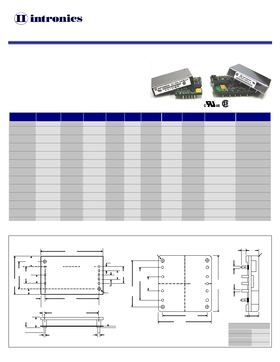
Q & H SERIES
DC/DC MODULES
All dimensions are in inches [mm]
Pins 4 & 8 (Q150) are dia. 0.062 [1.57]
Pins 5 & 9 (H) are dia. 0.08 [2.03]
Tolerances
Inches
Millimeters
� XX �0.020
� X �0.5
� XXX �0.010 � XX �0.25
Pin: �0.002
�0.05
Approval Pending
BOTTOM VIEW
Q FAMILY
� Output current limit and short circuit protection
� High power density up to 90W/inch�
� MTBF of up to 1,600,000 hours @ 50�C (Bellcore)
� Remote On/Off pin control (Negative Logic available)
� Meets Basic Insulation requirements of EN60950 (Open Frame Q and H Families)
� UL 60950 recognized, TUV EN60950 and CSA C22.2 No. 60950-00 Certified (Approvals Pending)
� Meets conducted limits of FCC Class B and CEI IEC61204-3 Class B with external filter
All other pins are dia. 0.040 [1.02]
Case: Aluminum material with anodized finish
Weight: 39.5g (1.4oz) for Q and 60g (2.3oz) for H Series
BOTTOM VIEW
H FAMILY
Intronics, Inc. 1400 Providence Highway, Building 2, Norwood, MA 02062-5015
�
Phone: 1-800-367-0004, 1-781-551-5500
�
Fax: 1-781-551-5555 Rev. C
Specifications & Features Summary
� No minimum load required
� -40�C to +85�C ambient operation
� Output adjustment +/-10% range
� 1500V, 10M input-to-output isolation
� Unique Flat Transformer Technology
� Complimentary Circuits
� Over Temperature protection
� Output remote sense feature
� Input undervoltage lockout
The Q and H Families of high power, high density DC/DC converters offer power levels of up to 150 Watt in Industry-Standard Quarter-brick and Half-brick Pinouts. With a wide input voltage range
and outputs, ranging from 1.5 to 24 Volts, these converters provide versatility without sacrificing the board space. All models feature an input filter, input undervoltage lockout, overtemperature
protection, output current limiting and short circuit protection. Various packaging techniques offer versatility for multitude of applications and requirements. The use of patented design concepts
facilitates maximum power delivered with the highest efficiency of up to 93%. All converters combine creative design practices with highly derated power devices to achieve very high reliability,
high performance and low cost solution to systems designers.
0.09
[2.29]
2.00
[50.80]
1.45
[38.8]
0.15
[3.81]
0.30
[7.62]
1.19
[30.23] 0.60
[15.24]
0.30
[7.62]
0.13
[3.30]
0.20
[5.08]
1 Vin +
2 On/Off
3 Vin -
Vo - 4
Sense - 5
Trim 6
0.425
[10.80]
Sense + 7
Vo + 8
2.30
[58.40]
0.14
[3.56]
0.15
[3.81]
0.60
[15.24]
MOUNTING INSERTS
M3 X .05 THRU. 2 PLS.
SIDE VIEW
0.46 max.
[11.7]
2.002
[51.30]
MOUNTING INSERTS
0.13
[3.30]
x 0.040
[1.02]
x 0.062
[1.52] 2 pl.
MOUNTING INSERTS
M3 X 0.5 THRU 4PL.
2.00
[50.80]
1.40
[35.56]
0.60
[15.24]
2.40
[61.00]
1.90
[48.26]
2.28
[57.90]
0.40
[10.16]
0.04
[1.02] 7 pl.
0.08
[2.03] 2 pl.
0.18 min.
[4.60]
2*R1.5
1 Vin+
Vo+ 9
Trim 7
Sense - 6
Vo- 5
Sense + 8
4 Vin-
3 NC (H120)
or Case
2 On/Off
0.50
[12.70]
H 120 OPEN FRAME
CONSTRUCTION