 | –≠–ª–µ–∫—Ç—Ä–æ–Ω–Ω—ã–π –∫–æ–º–ø–æ–Ω–µ–Ω—Ç: DAC488HR | –°–∫–∞—á–∞—Ç—å:  PDF PDF  ZIP ZIP |

Q U I C K F I N D
tel: 440-439-4091
fax: 440-439-4093
248
sales@iotech.com
www.iotech.com
the smart approach to instrumentation
TM
Æ
IEEE 488 Data Acquisition Instruments
Features
∑
Two or four isolated 16-bit outputs
∑
100-kHz/channel update rate
∑
480 Ksamples/channel max buffer
∑
±
1,
±
2,
±
5, &
±
10 VFS programmable
unipolar & bi-polar output ranges
∑
One-shot, step, burst, waveform, &
continuous output modes
∑
GET, external TTL, IEEE command,
& time event trigger sources
∑
ASCII, binary, integer decimal, & hexa-
decimal data formats
∑
Standard sine, square, & triangle
waveform generation
∑
500 VDC channel-to-channel isolation
∑
Eight digital inputs & eight digital
outputs
∑
100 mA high-current outputs
∑
LabVIEW
Æ
drivers
The DAC488HR
TM
is an IEEE 488 program-
mable 16-bit D/A converter. It can be
configured with either two or four output
channels, which are optically isolated from
each other and from IEEE 488 common
by up to 500 VDC. Each channel is inde-
pendently programmable for 1, 2, 5, or 10
VFS unipolar or bipolar output, specified
as either bits or volts in ASCII, integer,
hexadecimal, or binary format. Multiple
output modes, multiple clock and trigger
sources, and buffer management enable
the DAC488HR to function as a precision
voltage source, a function generator, or
an arbitrary waveform generator.
Waveforms captured by IOtech's 16-bit,
100-kHz ADC488A series (see p. 243) digi-
tizers can be edited and transferred to the
DAC488HR for output. The ADC488A
TM
series and DAC488HR in combination
form a powerful waveform I/O system.
Typical applications include transducer
simulation, disk drive testing, vibration
analysis, and materials testing.
DAC488HR
TM
16-bit D/A Converter with Digital I/O & IEEE 488
Burst Mode. Functionally identical to step
mode, except that waveforms rather than
single values are output.
Waveform Mode. Based on recognition
of a trigger, the waveform buffer is output
for a specified number of cycles.
Continuous Mode. Data is continuously
input from the IEEE 488 bus and output to
an analog channel at rates up to 200 Kbytes/s
upon the detection of a specified trigger.
This mode is ideally suited for audio, speech,
and other applications that require long
duration waveforms.
Trigger Modes
The DAC488HR's five trigger modes sup-
port a wide variety of applications.
Bus Control Mode. Each port is programmed
to output a specified value under direct
control from the IEEE 488 bus. This mode is
useful for maintaining an initial value until
a specified condition occurs.
Step Mode. When a specified trigger is
detected, a value is output from the
buffer, and the DAC488HR is automati-
cally re-armed until the specified buffer
count is reached. The last specified buffer
value is held as the output.
+ -
+ -
+ -
+ -
IEEE
Filter488
DAC488HR/2
SCSI488/S
DAC488HR
IEEE 488
controller
Up to 13 IEEE 488 devices
2- or 4-channel 16-bit,
isolated 100-kHz
analog outputs
8 digital
outputs
8 digital
inputs
DAC488HR
CH1 CH2 CH3 CH4
The versatile DAC488HR functions as a voltage source, function generator, and an arbitrary
waveform generator

249
Q U I C K F I N D
the smart approach to instrumentation
TM
Æ
IEEE 488 Data Acquisition Instruments
tel: 440-439-4091
fax: 440-439-4093
sales@iotech.com
www.iotech.com
DAC488HR
TM
General Information
DAC488HR Design
Four independent analog output modules are optically isolated
from the IEEE 488 bus, digital circuitry, earth ground, and
chassis common by up to 500 VDC. Each module consists of a
microcontroller and expandable data buffer. A common update
clock is shared by all ports, ensuring synchronization. Four
internal clock sources are available to meet a wide variety of
applications including CD and DAT testing. An external clock
source (up to 10 MHz) allows synchronization to an external
frequency reference and can be used to synchronize the
DAC488HR to the ADC488A series (see p. 243) digitizers for
stimulus/response applications.
Multiple Trigger Sources
All DAC488HR ports share a common trigger source, ensuring
multi-channel synchronization for applications with critical
time and phase relationships. Trigger sources for the DAC488HR
include trigger command, IEEE 488 Group Execute Trigger
(GET), and external TTL (rising or falling edge) signal input.
Triggers can also be initiated on periodic intervals from 2 ms to
65,535 ms, specified in 1 ms increments. The DAC488HR pro-
vides a delayed TTL-level trigger output for stimulus/response
applications in which the device under test (DUT) must attain a
steady state prior to measurement. This function allows users to
specify a time delay, in update clock counts from 1 to 65,535,
between the DAC488HR's output and the trigger signal's output.
Multiple Clock Sources
The DAC488HR features four internal clock sources and accommo-
dates an external clock source (up to 10 MHz) for updating the
output ports. A 16-bit counter is used to provide update rates to
meet application requirements. For example, the 200-kHz clock
and the 5-MHz clock can be divided down to any rate between 3 Hz
and 100 kHz for general purpose applications; the
5.6448-MHz clock can simulate 44.1-kHz audio CD signals; and the
6.144-MHz can simulate 48-kHz audio DAT signals. For synchro-
nizing external circuitry to DAC488HR output, an update clock
signal is also provided.
Buffer Management
The DAC488HR's step, burst, waveform, and continuous trigger
output modes can be used with flexible buffer management
functions to output stepped voltages, any one of five standard
waveforms, or user-defined arbitrary waveforms. Waveforms are
loaded from the IEEE 488 bus into the DAC488HR's resident
8 Ksample buffer at rates up to 500 Kbytes/s.
To output standard predefined sine, square, and triangle wave-
forms, the user specifies the starting memory location, number
of samples, max/min values, duty cycle, and the number of
times the cycle is to be repeated or "looped." The "looping"
function outputs specified buffer segments up to the full avail-
able buffered size for repetition up to 65,535 times. This con-
serves memory space by allowing long periodic waveforms to be
defined in a single cycle. Additionally, for applications that
exceed the DAC488HR's internal buffer capacity, waveforms
can be output continuously from an IEEE 488 controller at up to
200 Kbytes/s via the IEEE 488 bus.
Nonvolatile Storage
The DAC488HR uses resident nonvolatile random access
memory (NVRAM) to store the calibration constants deter-
mined during digital calibration, and to store its power-up
default configuration.
Each DAC488HR output port features a separate microprocessor and
buffer memory for independent waveform management
D/A
channel 3
D/A
channel 1
Isolated
analog
output
Non-isolated
digital I/O
IEEE 488
interface
Internal
peripheral
interface
bus
D/A
channel 2
D/A
channel 4
Non-
isolated
Isolated
Power
source 1
Power
source 2
Power
source 3
Power
source 4
PS
main
Main
processor
digital
circuitry

Q U I C K F I N D
tel: 440-439-4091
fax: 440-439-4093
250
sales@iotech.com
www.iotech.com
the smart approach to instrumentation
TM
Æ
IEEE 488 Data Acquisition Instruments
DAC488HR
TM
General Information
Support Software
The DAC488HR series is shipped with
QuickBasic
Æ
and C sample programs.
Free VIs (Virtual Instruments) are avail-
able from IOtech that enable the immedi-
ate integration of the DAC488HR series
into existing LabVIEW
Æ
applications. Each
of these ready-to-use VIs provide immedi-
ate access to common DAC488HR func-
tions, and both include source code that
can be modified to meet specific
application requirements.
Stimulus/Response System
When configured with an ADC488A se-
ries A/D converter, the DAC488HR is well-
suited for stimulus/response testing. For
synchronous operation in which acquisi-
tion must begin simultaneously with the
stimulus output, the DAC488HR's TTL
trigger output is connected directly with
the ADC488A's TTL trigger input; for non-
synchronous operation in which acquisi-
tion must begin at a specified time after
the stimulus output, the DAC488HR's trig-
ger output can be "delayed" up to 65,535
update clock counts.
Multi-DAC488HR
Synchronization
Multiple DAC488HRs can be configured
in master/slave mode to synchronously
output data either from their internal
buffers, or continuously from the IEEE
488 bus. When daisy-chained together
using the CA-112 master-slave cable, the
number of DAC488HRs in a system is
limited only by the number of available
IEEE 488 addresses, and the trigger "la-
tency" between each unit is 60 ns*. For
applications that require non-additive trig-
ger latencies, the DAC488HRs can be con-
figured in parallel, limiting total system
trigger latency to 60 ns.
Continuously output a standard
wave function under program
control
Output a series of voltage values
based on TTL triggers
Initiate a trigger delay from 1 to
65,535 update clock pulses
Synchronously output multiple
waveforms under program
control
Output a standard waveform
acquired by the ADC488A series
digitizer
Continuously output a large
arbitrary waveform from the IEEE
488 bus at up to 200 Kbytes/s
Standard function generator
outputs for general purpose
applications
Sequenced V out for controlling
power supplies or other analog
programmable instruments
Allows a device under test (DUT)
to attain a steady state prior to
measurement
Ideal for stimulus/response
applications with critical time
and phase relationships
Ideal for simulating complex
signals such as EKGs and
contact bounce
For audio system testing, speech
research, and other tests
requiring long-time waveform
generation
Waveform(s)
Functional Requirement
Typical Application
T1
T2
T3
T4
trigger event
trigger delay
Analog output signal
* A system with one master and three slave units will have a total system trigger latency of 180 ns
251
Q U I C K F I N D
the smart approach to instrumentation
TM
Æ
IEEE 488 Data Acquisition Instruments
tel: 440-439-4091
fax: 440-439-4093
sales@iotech.com
www.iotech.com
DAC488HR
TM
Specifications & Ordering Information
Specifications
Analog Output
Number of Channels: 2 or 4
DC Output Voltage/Resolution
1V Range:
±
1V, 30.5
µ
V/bit
2V Range:
±
2V, 61
µ
V/bit
5V Range:
±
5V, 152
µ
V/bit
10V Range:
±
10V, 305
µ
V/bit
DC Output Current:
±
10 mA max
Accuracy (25
±
5∞C)
1V Range:
±
0.02%
±
50
µ
V
2V Range:
±
0.02%
±
100
µ
V
5V Range:
±
0.02%
±
250
µ
V
10V Range:
±
0.02%
±
500
µ
V
Polarity: Unipolar or bipolar (software selectable)
Output Impedance: 10 Ohm
Zero Offset: 50 to 500
µ
V
Linearity: 0.005%
Differential Linearity: 0.001%
Update Rate: 100 Ksamples/s (max per channel); all signals from the data buffer
are 100 Ksamples/s max; any single channel from the IEEE 488 bus to output
is 100 Ksamples/s max; any two channels from the IEEE 488 bus to output are
50 Ksamples/s max; any two channels from the IEEE 488 bus to multiple
DAC488HR's are 20 Ksample/s
Settling Time: 6
µ
s to 0.003% FSR
Temperature Coefficient: (
±
0.002%
±
100
µ
V)/∞C; 0∞ to 20∞C, 20∞ to 30∞C, and 30∞
to 50∞C
Channel-to-Channel Isolation: 500V max
Channel-to-Digital Common and Chassis Isolation: 500V max
Connectors: DB9 (female) per channel; mating connector supplied
Digital I/O
Digital Inputs: 8 TTL level compatible, external TTL trigger, external TTL clock
input
Digital Outputs: 8 TTL level compatible, also configurable as open collector with
100 mA drive, and delayed trigger output signal, update clock output.
Connectors: DB15 (female) per input and output port; mating connector
supplied
IEEE 488 Specifications
Interface Subsets: SH1, AH1, T6, TE6, L4, LE4, SR1, PP0, RL0, DC1, DT2, C0,
and E2
Connector: Standard IEEE 488 connector with metric studs
Data Storage and Output
Data Buffer: 8 Ksamples standard (per channel); 128 Ksample option or 480 Ksample
option (per channel)
Data Format: ASCII, integer decimal, hexadecimal, and binary
Output Modes: Direct, step, burst, waveform, and continuous
Trigger Sources: GET, periodic time interval, external (TTL level), and command
Trigger Latency: Daisy chain mode; 60 ns (additive per unit) Parallel mode;
60 ns (non-additive system maximum)
General
Power: 90 to 125 or 210 to 250 VAC, 50/60 Hz; 20 VA max
Environment: 0∞ to 50∞C; 0 to 95% RH, non-condensing
Controls: Power switch, external dip switch for IEEE address
Dimensions: 425 mm W x 305 mm D x 45 mm H (16.75" x 12" x 1.75")
Weight: 3.6 kg (7.9 lbs)
Supplied Accessories: Analog output connector, digital I/O port connector
Ordering Information
Description
Part No.
Isolated 2-channel converter with 8 Ksample memory
per channel; includes analog output connector;
digital I/O port connector; and rack-mount kit
DAC488HR/2
Isolated 4-channel converter with 8 Ksample memory
per channel; includes analog output connector;
digital I/O port connector; and rack-mount kit
DAC488HR/4
128 Ksample memory expansion for one channel
MEMX3*
480 Ksample memory expansion for one channel
MEMX4*
Shielded cable with male DB9 connector
for analog output, 6 ft.
CA-89
Shielded cable with male DB15 connector
for digital I/O, 6 ft.
CA-90
DAC488HR master/slave cable, 3 ft.
CA-112
Shielded IEEE 488 cable, 6 ft.
CA-7-3
LabVIEW
Æ
driver
LBV/DAI
Related Products
Hardware
ADC488/16A
p. 243
ADC488/8SA
p. 246
DAC488
p. 252
Personal488 series
p. 263
Serial Communication Boards
p. 297
* Memory expansion modules are ordered on a per channel basis. They must be
installed and calibrated at the factory. Contact factory for details.
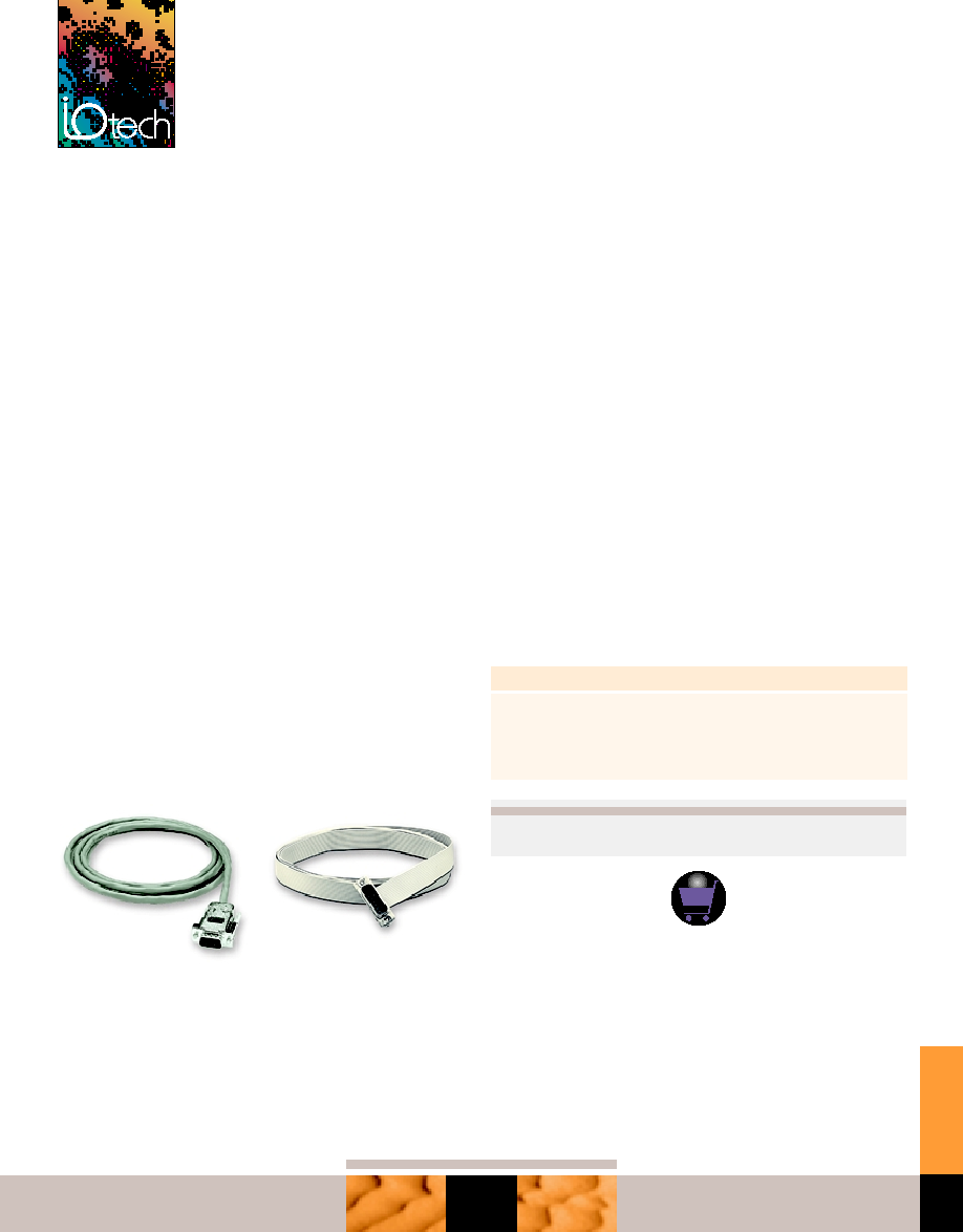
CA-89, Shielded cable with male
DB9 connectors for DAC488HR
analog output, 6 ft.
CA-90, Ribbon cable with male
DB15 connector for DAC488HR
digital I/O, 6 ft.
Q U I C K F I N D
For up-to-date information on products, and to order online, visit the IOtech Web
site and enter the corresponding page number in the QUICK FIND field.
SHOP
ON
LINE