I
F(AV)
Rectangular waveform
100
A
@ T
C
91
∞C
I
DC
Maximum
141
A
V
RRM
15
V
I
FSM
@ tp = 5 µs sine
5000
A
V
F
@
100 Apk typical
0.38
V
@ T
J
125
∞C
T
J
range
- 55 to 125
∞C
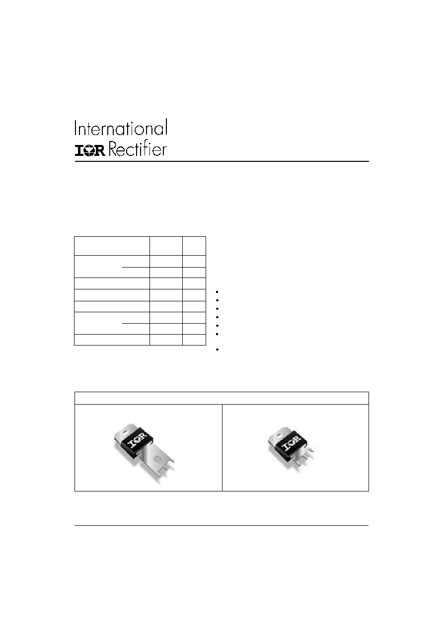
SCHOTTKY RECTIFIER
100 Amp
100BGQ015
100BGQ015J
Bulletin PD-20995 rev. F 12/02
1
www.irf.com
Characteristics
100BGQ015
Units
The 100BGQ015 Schottky rectifier has been optimized for ultra
low forward voltage drop specifically for the OR-ing of parallel
power supplies. The proprietary barrier technology allows for
reliable operation up to 125∞ C junction temperature. Typical
applications are in parallel switching power supplies, converters,
reverse battery protection, and redundant power subsystems.
125∞C T
J
operation (V
R
< 5V)
Optimized for OR-ing applications
High frequency operation
Ultra low forward voltage drop
Continuous High Current operation
Guard ring for enhanced ruggedness and long term
reliability
PowIRtab
TM
package
Major Ratings and Characteristics
Description/ Features
Case Styles
100BGQ015
100BGQ015J
100BGQ015, 100BGQ015J
2
Bulletin PD-20995 rev. F 12/02
www.irf.com
V
FM
Forward Voltage Drop (1) (2)
0.34 0.37
V
@ 50A
0.42 0.46
V
@ 100A
0.26 0.29
V
@ 50A
0.38 0.42
V
@ 100A
I
RM
Reverse Leakage Current (1)
7
18
mA
T
J
= 25 ∞C
580 870
mA
T
J
= 100 ∞C
480 700
mA
T
J
= 100 ∞CV
R
= 12V
1
1.2
A
T
J
= 125 ∞CV
R
= 5V
V
F(TO)
Threshold Voltage
0.155
V
T
J
=
T
J
max.
r
t
Forward Slope Resistance
2.45
m
C
T
Max. Junction Capacitance
3800
pF
V
R
= 5V
DC
, (test signal range 100Khz to 1Mhz) 25 ∞C
L
S
Typical Series Inductance
3.5
nH
Measured from tab to mounting plane
dv/dt Max. Voltage Rate of Change
10000
V/ µs
(Rated V
R
)
T
J
Max. Junction Temperature Range
-55 to 125
∞C
T
stg
Max. Storage Temperature Range
-55 to 150
∞C
R
thJC
Max. Thermal Resistance Junction
0.50
∞C/W DC operation
to Case
R
thCS
Typical Thermal Resistance, Case to
0.20
∞C/W Mounting surface , smooth and greased
Heatsink
wt
Approximate Weight
5 (0.18)
g (oz.)
T
Mounting Torque
Min.
1.2 (10)
Max.
2.4 (20)
Case Style
PowIRtab
TM
N*m
(Ibf-in)
Thermal-Mechanical Specifications
Parameters
100BGQ
Units
Conditions
Part number
100BGQ015
V
R
Max. DC Reverse Voltage (V)
@ T
J
= 100 ∞C
15
V
R
Max. DC Reverse Voltage (V)
@ T
J
= 125 ∞C
5
Voltage Ratings
I
F(AV)
Max. Average Forward Current
100
A
50% duty cycle @ T
C
= 91∞C, rectangular wave form
I
F(RMS)
RMS Forward Current
141
A
T
C
= 88∞C
I
FSM
Max. Peak One Cycle Non-Repetitive
5000
5µs Sine or 3µs Rect. pulse
Surge Current
1000
10ms Sine or 6ms Rect. pulse
E
AS
Non-Repetitive Avalanche Energy
9
mJ
T
J
= 25 ∞C, I
AS
= 2 Amps, L = 4.5 mH
I
AR
Repetitive Avalanche Current
2
A
Current decaying linearly to zero in 1 µsec
Frequency limited by T
J
max. V
A
= 3 x V
R
typical
Parameters
100BGQ
Units
Conditions
Absolute Maximum Ratings
A
Following any rated
load condition and
with rated V
RRM
applied
T
J
= 25 ∞C
T
J
= 125 ∞C
V
R
= rated V
R
Electrical Specifications
Parameters
100BGQ
Units
Conditions
Typ.
Max.
(1) Pulse Width < 300µs, Duty Cycle < 2%
(2) V
FM
= V
F(TO)
+ r
t
x I
F

100BGQ015, 100BGQ015J
3
Bulletin PD-20995 rev. F 12/02
www.irf.com
Fig. 2 - Typical Values of Reverse Current
Vs. Reverse Voltage
Fig. 3 - Typical Junction Capacitance
Vs. Reverse Voltage
Fig. 4 - Maximum Thermal Impedance Z
thJC
Characteristics
Fig. 1 - Maximum Forward Voltage Drop Characteristics
1
10
100
1000
0
0.25
0.5
0.75
1
1.25
1.5
F
FM
Forward Voltage Drop - V (V)
In
st
a
n
t
a
n
e
ou
s F
o
r
w
a
r
d
Cu
r
r
e
n
t
- I
(
A
)
T = 125∞C
T = 100∞C
T = 25∞C
J
J
J
1
10
100
1000
0
2
4
6
8
10
12
14
16
R
R
75∞C
50∞C
25∞C
Re
ve
r
s
e
C
u
r
r
e
n
t -
I
(
m
A
)
Reverse Voltage - V (V)
T = 100∞C
J
1000
10000
0
2
4
6
8
10
12
14
16
R
T
J
u
n
c
t
i
on
Cap
a
c
i
t
a
n
c
e - C (
p
F
)
Reverse Voltage - V (V)
T = 25∞C
J
0.01
0.1
1
0.00001
0.0001
0.001
0.01
0.1
1
10
100
th
J
C
t , Rectangular Pulse Duration (Seconds)
Single Pulse
(Thermal Resistance)
1
T
h
e
r
m
a
l
I
m
p
e
da
n
c
e
Z
(
∞
C
/
W
)
Notes:
1. Duty factor D = t / t
2. Peak T = P x Z + T
1
2
J
thJC
C
DM
D = 0.75
D = 0.50
D = 0.33
D = 0.25
D = 0.20
2
t
1
t
P
DM
100BGQ015, 100BGQ015J
4
Bulletin PD-20995 rev. F 12/02
www.irf.com
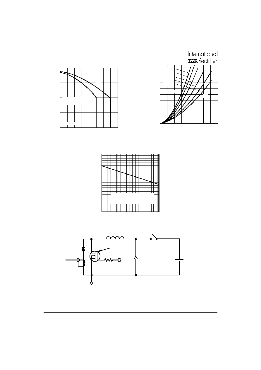
Fig. 8 - Unclamped Inductive Test Circuit
Fig. 5 - Maximum Allowable Case Temperature
Vs. Average Forward Current
Fig. 6 - Forward Power Loss Characteristics
Fig. 7 - Maximum Non-Repetitive Surge Current
FREE-WHEEL
DIODE
40HFL40S02
CURRENT
MONITOR
HIGH-SPEED
SWITCH
IRFP460
L
DUT
Rg = 25 ohm
Vd = 25 Volt
+
100
1000
10000
10
100
1000
10000
FS
M
N
o
n
-
R
e
p
e
t
i
t
i
v
e
S
u
r
g
e
C
u
r
r
e
n
t
- I
(A
)
p
At Any Rated Load Condition
And With Rated V Applied
Following Surge
RRM
Square Wave Pulse Duration - t (microsec)
(3) Formula used: T
C
= T
J
- (Pd + Pd
REV
) x R
thJC
;
Pd = Forward Power Loss = I
F(AV)
x V
FM
@ (I
F(AV)
/
D) (see Fig. 6);
Pd
REV
= Inverse Power Loss = V
R1
x I
R
(1 - D); I
R
@ V
R1
= 80% rated V
R
0
20
40
60
80
100
0
20
40
60
80 100 120 140 160
DC
A
v
e
r
a
g
e
P
o
we
r
L
o
ss - (
W
a
t
ts
)
F(AV)
RMS Limit
D = 0.20
D = 0.25
D = 0.33
D = 0.50
D = 0.75
Average Forward Current - I (A)
50
60
70
80
90
100
110
120
130
0
20
40 60
80 100 120 140 160
DC
All
o
w
a
ble
C
a
s
e
T
e
m
p
e
r
at
u
r
e
-
(
∞
C
)
F(AV)
Average Forward Current - I (A)
Square wave (D = 0.50)
5 V applied
see note (3)
