 | –≠–ª–µ–∫—Ç—Ä–æ–Ω–Ω—ã–π –∫–æ–º–ø–æ–Ω–µ–Ω—Ç: 10ETF10S | –°–∫–∞—á–∞—Ç—å:  PDF PDF  ZIP ZIP |

I
F(AV)
Sinusoidal waveform
10
A
V
RRM
range
1000 to 1200
V
I
FSM
160
A
V
F
@
10 A, T
J
= 25∞C
1.33
V
t
rr
@ 1A, 100A/µs
80
ns
T
J
range
- 40 to 150
∞C
Major Ratings and Characteristics
Characteristics
10ETF..S
Units
Description/Features
The 10ETF..S fast soft recovery QUIET
IR
rectifier
series has been optimized for combined short
reverse recovery time and low forward voltage
drop.
The glass passivation ensures stable reliable
operation in the most severe temperature and
power cycling conditions.
Typical applications are both:
output rectification and freewheeling in
inverters, choppers and converters
and input rectifications where severe
restrictions on conducted EMI should be met.
Package Outline
D
2
Pak (SMD-220)
FAST SOFT RECOVERY
RECTIFIER DIODE
1
I2149 rev. A 11/99
QUIET
IR
Series
10ETF..S
www.irf.com
V
F
< 1.33V @ 10A
t
rr
= 80ns
V
RRM
1000 to 1200V
2
10ETF..S QUIET
IR
Series
I2149 rev. A 11/99
www.irf.com
I
F(AV)
Max. Average Forward Current
10
A
@ T
C
= 125∞ C, 180∞ conduction half sine wave
I
FSM
Max. Peak One Cycle Non-Repetitive
160
10ms Sine pulse, rated V
RRM
applied
Surge Current
185
10ms Sine pulse, no voltage reapplied
I
2
t
Max. I
2
t for fusing
128
10ms Sine pulse, rated V
RRM
applied
180
10ms Sine pulse, no voltage reapplied
I
2
t Max. I
2
t for fusing
1800
A
2
s
t = 0.1 to 10ms, no voltage reapplied
Part Number
V
RRM
, maximum
V
RSM
, maximum non repetitive
I
RRM
peak reverse voltage
peak reverse voltage
150∞C
V
V
mA
10ETF10S
1000
1100
4
10ETF12S
1200
1300
Voltage Ratings
Absolute Maximum Ratings
Electrical Specifications
Recovery Characteristics
Parameters
10ETF..S
Units
Conditions
A
A
2
s
V
FM
Max. Forward Voltage Drop
1.33
V
@ 10A, T
J
= 25∞C
r
t
Forward slope resistance
22.9
m
T
J
= 150∞C
V
F(TO)
Threshold voltage
0.96
V
I
RM
Max. Reverse Leakage Current
0.1
T
J
= 25 ∞C
4
T
J
= 150 ∞C
Parameters
10ETF..S
Units
Conditions
V
R
= rated V
RRM
mA
t
rr
Reverse Recovery Time
310
ns
I
F
@ 10Apk
I
rr
Reverse Recovery Current
4.7
A
@ 25A/ µs
Q
rr
Reverse Recovery Charge
1.05
µC
@ 25∞C
S
Typical Snap Factor
0.6
Parameters
10ETF..S
Units
Conditions

3
10ETF..S QUIET
IR
Series
I2149 rev. A 11/99
www.irf.com
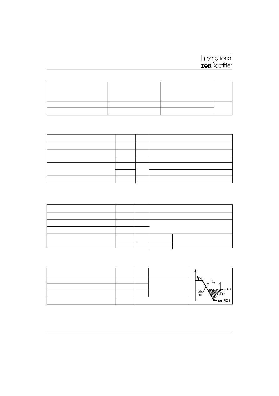
Fig. 1 - Current Rating Characteristics
Fig. 2 - Current Rating Characteristics
Fig. 3 - Forward Power Loss Characteristics
Fig. 4 - Forward Power Loss Characteristics
1 1 5
1 2 0
1 2 5
1 3 0
1 3 5
1 4 0
1 4 5
1 5 0
0
2
4
6
8
1 0
1 2
3 0 ∞
6 0 ∞
9 0 ∞
1 2 0 ∞
1 8 0 ∞
M
a
x
i
mu
m A
l
l
o
w
a
b
l
e
C
a
s
e
T
e
mp
e
r
a
t
u
r
e
(
∞
C
)
C o nd uc tio n A ng le
A v e ra g e F o rw a rd C ur re n t ( A )
1 0 E T F.. Se rie s
R ( D C ) = 1 .5 ∞C / W
thJ C
1 1 5
1 2 0
1 2 5
1 3 0
1 3 5
1 4 0
1 4 5
1 5 0
0
2
4
6
8
1 0
1 2
1 4
1 6
D C
3 0 ∞
6 0 ∞
9 0 ∞
1 2 0 ∞
1 8 0 ∞
M
a
x
i
m
u
m
A
l
l
o
w
a
b
l
e C
a
s
e
T
e
m
p
er
a
t
u
r
e (
∞
C)
Co nd uc tio n Pe rio d
A v e ra g e Fo rw a rd C u rre n t ( A )
1 0 E T F.. Se rie s
R ( D C ) = 1 .5 ∞ C / W
thJ C
0
2
4
6
8
1 0
1 2
1 4
1 6
0
2
4
6
8
1 0
R MS Lim it
1 8 0 ∞
1 2 0 ∞
9 0 ∞
6 0 ∞
3 0 ∞
C o nd uctio n A ng le
Average Forw ard Current (A)
M
a
x
i
mu
m
A
v
e
r
a
g
e
F
o
r
w
a
r
d
P
o
w
e
r
L
o
s
s
(
W
)
10.TF.. Series
T = 150 ∞C
J
0
4
8
1 2
1 6
2 0
2 4
0
2
4
6
8
1 0
1 2
1 4
1 6
D C
1 8 0 ∞
1 2 0 ∞
9 0 ∞
6 0 ∞
3 0 ∞
R M S L im it
C o nd u ction Pe rio d
A v e ra g e Fo rw a rd C u rre n t ( A )
M
a
x
i
mu
m A
v
e
r
a
g
e
F
o
r
w
a
r
d
P
o
w
e
r
L
o
s
s
(
W
)
1 0 E T F.. S e rie s
T = 1 5 0 ∞C
J
T
J
Max. Junction Temperature Range
- 40 to 150
∞C
T
stg
Max. Storage Temperature Range
- 40 to 150
∞C
R
thJC
Max. Thermal Resistance Junction
1.5
∞C/W
DC operation
to Case
R
thJA
Max. Thermal Resistance Junction
62
∞C/W
to Ambient (PCB Mount)**
T
s
Soldering Temperature
240
∞C
wt
Approximate Weight
2 (0.07)
g (oz.)
Case Style
D
2
Pak (SMD-220)
Thermal-Mechanical Specifications
Parameters
10ETF..S Units
Conditions
**When mounted on 1" square (650mm
2
) PCB of FR-4 or G-10 material 4 oz (140µm) copper 40∞C/W
For recommended footprint and soldering techniques refer to application note #AN-994
4
10ETF..S QUIET
IR
Series
I2149 rev. A 11/99
www.irf.com
Fig. 8 - Recovery Time Characteristics, T
J
= 25∞C
Fig. 9 - Recovery Time Characteristics, T
J
= 150∞C
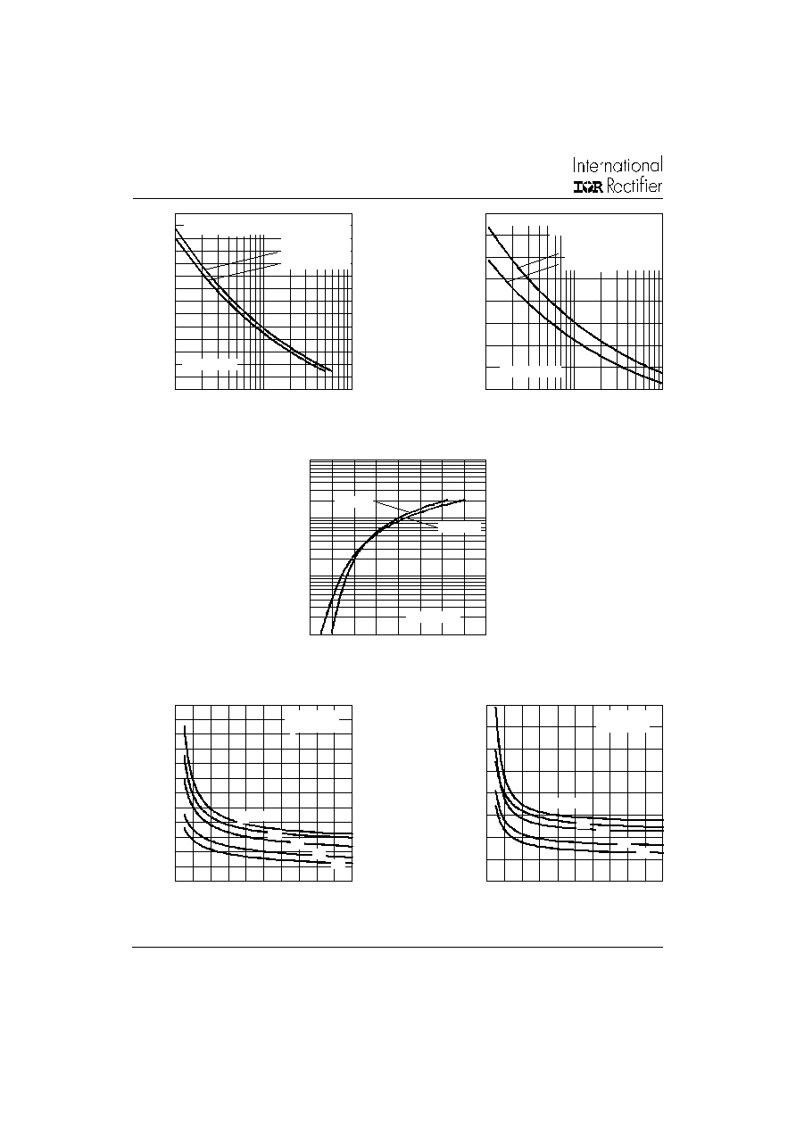
Fig. 7 - Forward Voltage Drop Characteristics
Fig. 5 - Maximum Non-Repetitive Surge Current
Fig. 6 - Maximum Non-Repetitive Surge Current
4 0
6 0
8 0
1 0 0
1 2 0
1 4 0
1 6 0
1 8 0
1
1 0
1 0 0
N um b e r O f E q ua l A m plitu de Hal f C y c l e C ur re nt P u ls e s (N )
P
e
ak
Hal
f
S
i
n
e
W
a
v
e
Fo
r
w
ar
d C
u
r
r
e
n
t
(
A
)
In itia l T = 1 5 0 ∞C
@ 6 0 H z 0 .0 0 8 3 s
@ 5 0 H z 0 .0 1 0 0 s
J
A t A n y R a t e d L o a d C o n d itio n A n d W ith
R a te d V A p p lie d Fo llo w in g S u rg e .
RRM
1 0ET F.. Series
4 0
6 0
8 0
10 0
12 0
14 0
16 0
18 0
20 0
0.0 1
0 .1
1
Pulse Train Duration (s)
P
e
ak
Hal
f
S
i
n
e
W
a
v
e
F
o
r
w
ar
d
C
u
r
r
e
n
t
(
A
)
V ersus Pulse Train Duration.
In itial T = 1 50∞C
No Voltage Reapplied
Rated V Reapplied
RR M
J
M a xim u m N o n R e pe titiv e Surg e C urre nt
1 0 E TF.. Se r ies
1
1 0
10 0
1 0 00
0.5
1
1. 5
2
2 .5
3
3 .5
4
4 .5
T = 25∞C
In
st
a
n
t
a
n
e
o
u
s F
o
r
w
a
r
d
C
u
r
r
e
n
t
(
A
)
Instan taneous Forward Voltage (V )
T = 150 ∞C
J
J
1 0ETF.. Ser ies
0
0 .1
0 .2
0 .3
0 .4
0 .5
0 .6
0
4 0
8 0
1 2 0
1 6 0
2 0 0
R a te O f F a ll O f Fo rw a rd C u rre n t - d i/ d t ( A / µs )
1 A
5 A
M
a
x
i
m
u
m
R
e
v
e
rs
e
R
e
c
o
v
e
ry
T
i
m
e
-
T
rr (
µ
s
)
8 A
2 A
I = 1 0 A
FM
1 0 E T F.. S e r ie s
T = 2 5 ∞C
J
0
0 .2
0 .4
0 .6
0 .8
0
4 0
8 0
1 2 0
1 6 0
2 0 0
Ra t e O f Fa ll O f F o rw a rd C u rre n t - d i/d t ( A / µ s)
1 A
5 A
M
a
x
i
m
u
m
R
e
v
e
rs
e
R
e
c
o
v
e
ry
T
i
m
e
-
T
rr (
µ
s
)
I = 1 0 A
FM
2 A
8 A
1 0 E T F.. S e rie s
T = 1 5 0 ∞ C
J
5
10ETF..S QUIET
IR
Series
I2149 rev. A 11/99
www.irf.com
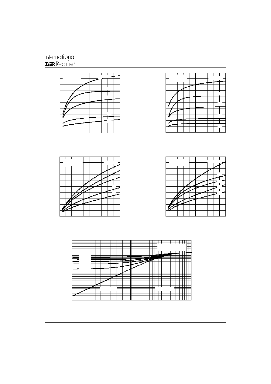
Fig. 14 - Thermal Impedance Z
thJC
Characteristics
Fig. 12 - Recovery Current Characteristics, T
J
= 25∞C
Fig. 13 - Recovery Current Characteristics, T
J
= 150∞C
Fig. 10 - Recovery Charge Characteristics, T
J
= 25∞C
Fig. 11 - Recovery Charge Characteristics, T
J
= 150∞C
0
0 .4
0 .8
1 .2
1 .6
2
0
4 0
8 0
1 2 0
1 6 0
2 0 0
R a t e O f F a ll O f Fo rw a rd C u rre n t - d i/ dt ( A / µ s)
1 A
5 A
M
a
x
i
m
u
m
Re
v
e
r
s
e
Re
c
o
v
e
r
y
C
h
a
r
g
e
-
Q
r
r
(
µ
C
)
I = 1 0 A
FM
2 A
8 A
1 0 E T F .. Se rie s
T = 2 5 ∞C
J
0
1
2
3
4
5
0
4 0
8 0
1 2 0
1 6 0
2 0 0
R a t e O f F a ll O f Fo rw a rd C ur re n t - d i/d t ( A /µ s)
1 A
5 A
M
a
x
i
mu
m
R
e
v
e
r
s
e
R
e
c
o
v
e
r
y
C
h
a
r
g
e
-
Q
r
r
(
µ
C
)
I = 1 0 A
F M
2 A
8 A
1 0 E T F.. S e r ie s
T = 1 5 0 ∞ C
J
0
4
8
1 2
1 6
2 0
0
4 0
8 0
1 2 0
1 6 0
2 0 0
M
a
x
i
m
u
m
R
e
v
e
rs
e
R
e
c
o
v
e
ry
C
u
rre
n
t
-
I
r
r
(
A
)
R a t e O f F a ll O f Fo rw a rd C u rre n t - d i/ d t ( A / µs )
1 A
5 A
8 A
2 A
I = 1 0 A
FM
1 0E T F.. Se ries
T = 2 5 ∞C
J
0
5
1 0
1 5
2 0
2 5
0
4 0
8 0
1 2 0
1 6 0
2 0 0
M
a
x
i
m
u
m
R
e
v
e
rs
e
R
e
c
o
v
e
ry
C
u
r
r
e
n
t
-
I
r
r (
A
)
R a t e O f Fa ll O f F o r w a r d C u rre n t - d i/ d t ( A / µ s)
1 A
5 A
I = 10 A
FM
8 A
2 A
1 0 ET F.. Se ries
T = 1 5 0 ∞C
J
0 . 0 0 1
0 . 0 1
0 . 1
1
1 0
0 . 0 0 1
0 . 0 1
0 . 1
1
1 0
Squa re W av e Pulse Du ration (s)
Stea dy Sta te V alue
(DC Op er ation)
Sin gle Pulse
th
J
C
Tr
a
n
s
i
e
n
t
Th
e
r
m
a
l
I
m
p
e
d
a
n
c
e
Z
(
∞
C/
W
)
D = 0 .50
D = 0 .33
D = 0 .25
D = 0 .17
D = 0 .08
1 0E TF. . Series