I
F(AV)
Rectangular waveform
175
A
@ T
C
107
∞C
I
DC
Maximum
248
A
V
RRM
45
V
I
FSM
@ tp = 5 µs sine
8700
A
V
F
@
175 Apk typical
0.61
V
@ T
J
150
∞C
T
J
range
- 55 to 150
∞C
SCHOTTKY RECTIFIER
175 Amp
175BGQ045
175BGQ045J
Bulletin PD-20710 rev. D 12/02
www.irf.com
Characteristics
175BGQ045
Units
The 175BGQ045 Schottky rectifier has been optimized for ultra
low forward voltage drop specifically for low voltage output in high
current AC/DC power supplies.
The proprietary barrier technology allows for reliable operation up
to 150∞C junction temperature. Typical applications are in
switching power supplies, converters, reverse battery protection,
and redundant power subsystems.
150∞C T
J
operation
High Frequency Operation
Ultra low forward voltage drop
Continuous High Current operation
Guard ring for enhanced ruggedness and long term
reliability
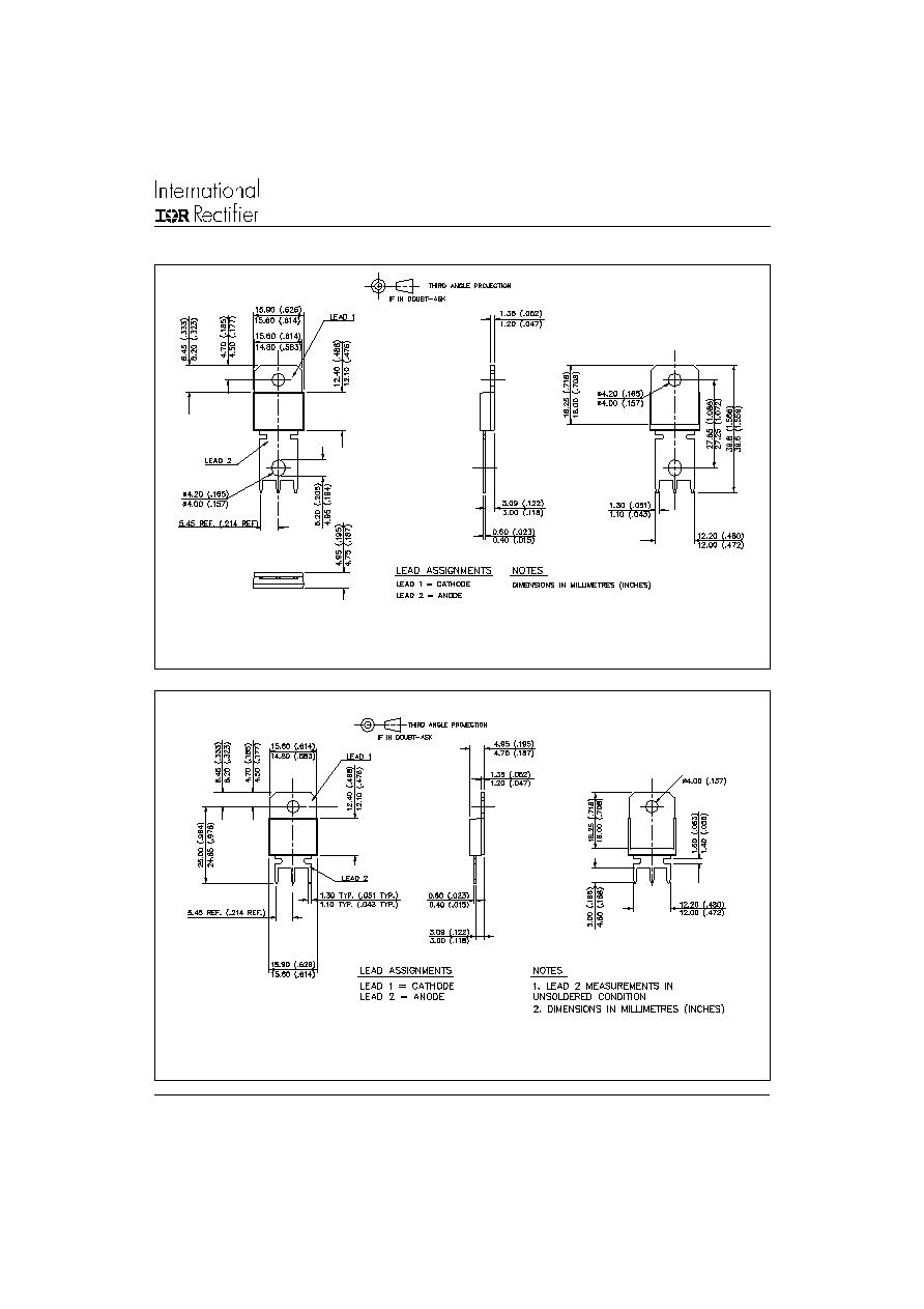
PowIRtab
TM
package
Major Ratings and Characteristics
Description/ Features
1
Case Styles
175BGQ045
175BGQ045J
175BGQ045, 175BGQ045J
Bulletin PD-20710 rev. D 12/02
www.irf.com
2
Voltage Ratings
V
FM
Forward Voltage Drop (1) (2)
0.53 0.56
V
@ 100A
0.64 0.69
V
@ 175A
0.48 0.52
V
@ 100A
0.61 0.64
V
@ 175A
I
RM
Reverse Leakage Current (1)
0.6
2
mA
T
J
= 25 ∞C
360 640
mA
T
J
= 125∞C
1200 2000 mA
T
J
= 150 ∞C
V
R
= 45V
V
F(TO)
Threshold Voltage
0.352
V
T
J
=
T
J
max.
r
t
Forward Slope Resistance
1.5
m
C
T
Max. Junction Capacitance
5600
pF
V
R
= 5V
DC
, (test signal range 100Khz to 1Mhz) 25 ∞C
L
S
Typical Series Inductance
3.5
nH
Measured from tab to mounting plane
dv/dt Max. Voltage Rate of Change
10000
V/ µs
(Rated V
R
)
T
J
Max. Junction Temperature Range
-55 to 150
∞C
T
stg
Max. Storage Temperature Range
-55 to 150
∞C
R
thJC
Max. Thermal Resistance Junction
0.25
∞C/W
DC operation
to Case
R
thCS
Typical Thermal Resistance, Case to
0.20
∞C/W
Mounting surface , smooth and greased
Heatsink
wt
Approximate Weight
5 (0.18)
g (oz.)
T
Mounting Torque
Min.
1.2 (10)
Max.
2.4 (20)
Case Style
PowIRtab
TM
N*m
(Ibf-in)
Thermal-Mechanical Specifications
Parameters
175BGQ
Units
Conditions
I
F(AV)
Max. Average Forward Current
175
A
50% duty cycle @ T
C
= 107∞C, rectangular wave form
I
F(RMS)
RMS Forward Current
248
A
T
C
= 104∞C
I
FSM
Max. Peak One Cycle Non-Repetitive
8700
5µs Sine or 3µs Rect. pulse
Surge Current
1550
10ms Sine or 6ms Rect. pulse
E
AS
Non-Repetitive Avalanche Energy
40
mJ
T
J
= 25 ∞C, I
AS
= 6 Amps, L = 2.0 mH
I
AR
Repetitive Avalanche Current
6
A
Current decaying linearly to zero in 1 µsec
Frequency limited by T
J
max. V
A
= 1.5 x V
R
typical
Parameters
175BGQ
Units
Conditions
Absolute Maximum Ratings
A
Following any rated
load condition and
with rated V
RRM
applied
T
J
= 25 ∞C
V
R
= rated V
R
Electrical Specifications
Parameters
175BGQ
Units
Conditions
Typ. Max.
(1) Pulse Width < 300µs, Duty Cycle < 2%
(2) V
FM
= V
F(TO)
+ r
t
x I
F
Part number
175BGQ045
V
R
Max. DC Reverse Voltage (V)
V
RWM
Max. Working Peak Reverse Voltage (V)
45
T
J
= 150 ∞C

175BGQ045, 175BGQ045J
3
Bulletin PD-20710 rev. D 12/02
www.irf.com
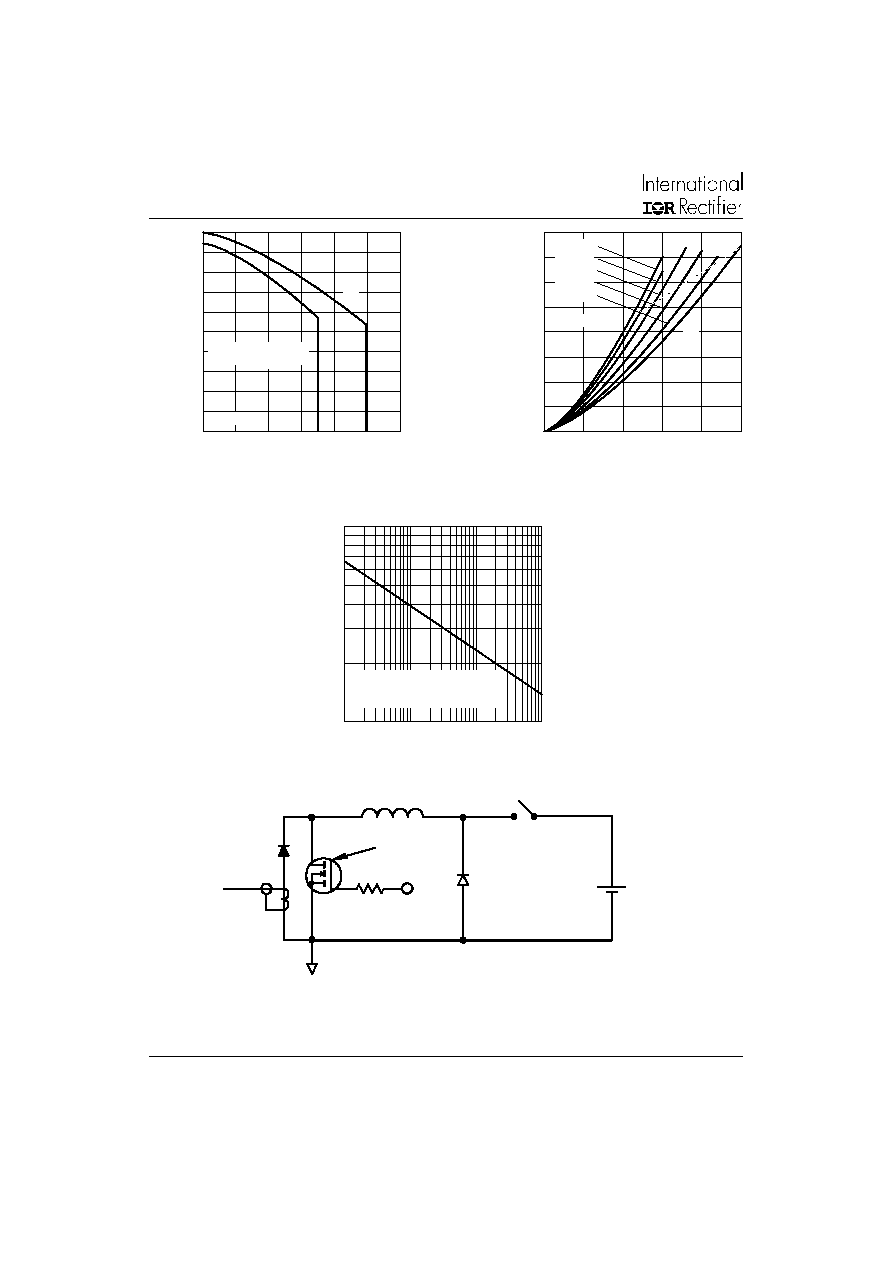
Fig. 2 - Typical Values of Reverse Current
Vs. Reverse Voltage
Fig. 3 - Typical Junction Capacitance
Vs. Reverse Voltage
Fig. 4 - Maximum Thermal Impedance Z
thJC
Characteristics
Fig. 1 - Maximum Forward Voltage Drop Characteristics
1
10
100
1000
0
0.2
0.4
0.6
0.8
1
1.2
1.4
F
FM
T = 150∞C
T = 125∞C
T = 25∞C
J
J
J
Forward Voltage Drop - V (V)
I
n
s
t
a
n
t
a
n
e
o
u
s
F
o
rw
a
r
d
C
u
rr
e
n
t
-
I
(
A
)
0.01
0.1
1
10
100
1000
10000
0
5
10 15 20 25 30 35 40 45
R
R
125∞C
100∞C
75∞C
50∞C
25∞C
R
e
v
e
r
s
e Cu
r
r
en
t
-
I
(
m
A
)
Reverse Voltage - V (V)
T = 150∞C
J
1000
10000
0
10
20
30
40
50
R
T
J
u
n
c
t
i
o
n
Cap
a
c
i
t
a
n
c
e - C (
p
F
)
Reverse Voltage - V (V)
T = 25∞C
J
0.01
0.1
1
0.00001
0.0001
0.001
0.01
0.1
1
10
th
J
C
t , Rectangular Pulse Duration (Seconds)
Single Pulse
(Thermal Resistance)
1
T
h
e
r
ma
l
Imp
e
d
a
n
c
e
Z
(
∞
C
/
W
)
Notes:
1. Duty factor D = t / t
2. Peak T = P x Z + T
1
2
J
thJC
C
DM
D = 0.75
D = 0.50
D = 0.33
D = 0.25
D = 0.20
2
t
1
t
P
DM
175BGQ045, 175BGQ045J
Bulletin PD-20710 rev. D 12/02
www.irf.com
4
Fig. 8 - Unclamped Inductive Test Circuit
Fig. 5 - Maximum Allowable Case Temperature
Vs. Average Forward Current
Fig. 6 - Forward Power Loss Characteristics
Fig. 7 - Maximum Non-Repetitive Surge Current
(3) Formula used: T
C
= T
J
- (Pd + Pd
REV
) x R
thJC
;
Pd = Forward Power Loss = I
F(AV)
x V
FM
@ (I
F(AV)
/
D) (see Fig. 6);
Pd
REV
= Inverse Power Loss = V
R1
x I
R
(1 - D); I
R
@ V
R1
= 80% rated V
R
FREE-WHEEL
DIODE
40HFL40S02
CURRENT
MONITOR
HIGH-SPEED
SWITCH
IRFP460
L
DUT
Rg = 25 ohm
Vd = 25 Volt
+
50
60
70
80
90
100
110
120
130
140
150
0
50
100
150
200
250
300
DC
Al
l
o
w
a
b
l
e
C
a
s
e
T
e
m
p
e
r
a
t
u
r
e
-
(
∞
C
)
F(AV)
Average Forward Current - I (A)
see note (3)
Square wave (D = 0.50)
80% Rated V applied
R
0
25
50
75
100
125
150
175
200
0
50
100
150
200
250
DC
A
v
er
a
g
e Pow
e
r
L
o
s
s
- (
W
at
t
s
)
F(AV)
RMS Limit
D = 0.20
D = 0.25
D = 0.33
D = 0.50
D = 0.75
Average Forward Current - I (A)
1000
10000
10
100
1000
10000
FS
M
N
o
n
-
R
e
p
e
t
i
t
i
v
e
S
u
r
g
e
Cu
r
r
e
n
t
-
I
(
A
)
p
At Any Rated Load Condition
And With Rated V Applied
Following Surge
RRM
Square Wave Pulse Duration - t (microsec)