 | ÐлекÑÑоннÑй компоненÑ: 19MT050XF | СкаÑаÑÑ:  PDF PDF  ZIP ZIP |
Äîêóìåíòàöèÿ è îïèñàíèÿ www.docs.chipfind.ru
1
19MT050XF
Bulletin I27128 Rev.C 07/03
Absolute Maximum Ratings
I
D
Continuos Drain Current @ V
GS
= 10V
@ T
C
= 25°C
31
A
@ T
C
= 100°C
19
I
DM
Pulsed Drain Current
(1)
124
P
D
Maximum Power Dissipation
@ T
C
= 25°C
1140
W
@ T
C
= 100°C
456
V
GS
Gate-to-Source Voltage
± 30
V
V
ISOL
RMS Isolation Voltage, Any Terminal to Case, t = 1 min
2500
dv/dt
Peak Diode Recovery dv/dt
(3)
15
V/ ns
Parameters
Max
Units
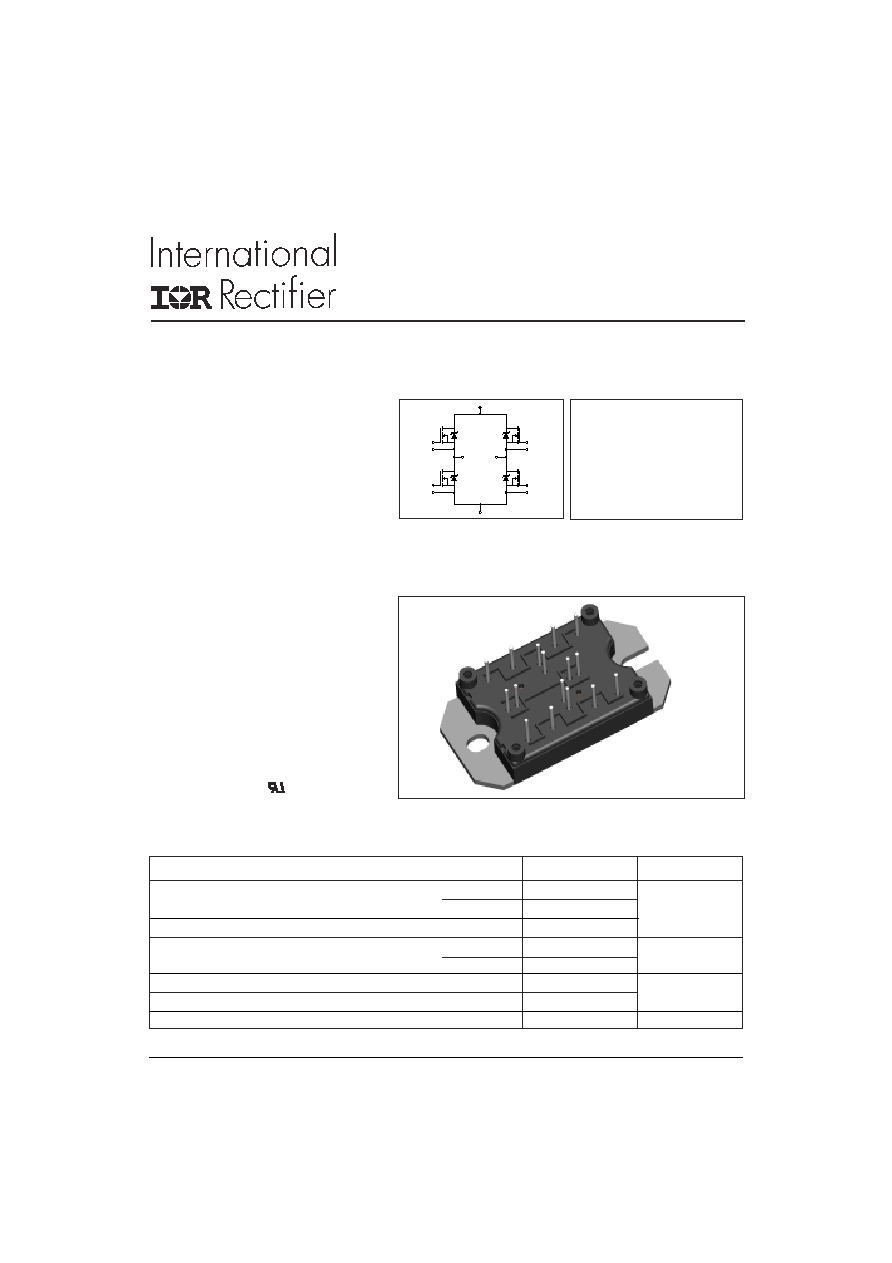
HEXFET
®
Power MOSFET
Low On-Resistance
High Performance Optimised Built-in Fast
Recovery Diodes
Fully Characterized Capacitance and
Avalanche Voltage and Current
Aluminum Nitride DBC
Very Low Stray Inductance Design for
High Speed Operation
Features
"FULL-BRIDGE" FREDFET MTP
Low Gate Charge Qg results in Simple
Drive Requirement
Improved Gate, Avalanche and Dynamic
dv/dt Ruggedness
Low Trr and Soft Diode Reverse Recovery
Optimized for Welding, UPS and SMPS
Applications
Outstanding ZVS and High Frequency
Operation
Direct Mounting to Heatsink
PCB Solderable Terminals
Very Low Junction-to-Case Thermal Resistance
UL Approved E78996
Benefits
M
MTP
www.irf.com
31 A
V
DSS
= 500V
19MT050XF
Bulletin I27128 Rev.C 07/03
2
www.irf.com
g
fs
Forward Transconductance
26
S
V
DS
= 50V, I
D
= 19A
Q
g
Total Gate Charge
105
160
nC
I
D
= 31A
Q
gs
Gate-to-Source Charge
36
55
V
DS
= 400V
Q
gd
Gate-to-Drain ("Miller") Charge
46
70
V
GS
= 10V
(4)
t
d(on)
Turn-on Delay Time
49
74
ns
I
D
= 31A
t
d(off)
Turn-off Delay Time
80
120
V
DS
= 250V
t
r
Rise Time
165
250
V
GS
= 10V
t
f
Fall Time
76
115
R
G
= 4.3
C
iss
Input Capacitance
4808 7210
pF
V
GS
= 0V
C
oss
Output Capacitance
1165 1750
V
DS
= 25V
C
rss
Reverse Transfer Capacitance
40
60
f = 1.0 MHz
V
(BR)DSS
Drain-to-Source Breakdown Voltage
500
V
V
GS
= 0V, I
D
= 250µA
V
(BR)DSS
/ Temperature Coeff. of
0.48
V/°C I
D
= 4mA, reference to T
J
= 25°C
T
J
Breakdown Voltage
R
DS(ON)
Static Drain-to-Source On-Resistance
0.19 0.22
V
GS
= 10V, I
D
= 19A
(4)
0.21 0.25
V
GS
= 10V, I
D
= 31A
V
GS(th)
Gate Threshold Voltage
3.0
6.0
V
V
DS
= V
GS
, I
D
= 250µA
I
DSS
Drain-to-Source Leakage Current (6)
50
µA
V
DS
= 500V, V
GS
= 0V
2
mA V
DS
= 400V, V
GS
= 0V, T
J
= 125°C
I
GSS
Gate-to-Source Forward Leakage
150
nA
V
GS
= 30V
Gate-to-Source Reverse Leakage
- 150
V
GS
= - 30V
Electrical Characteristics @ T
J
= 25°C (unless otherwise specified)
Parameters
Min Typ Max Units Test Conditions
Dynamic Characteristics @ T
J
= 25°C (unless otherwise specified)
Parameters
Min Typ Max Units Test Conditions
I
S
Continuous Source Current
31
A
MOSFET symbol
(Body Diode)
showing the
I
SM
Pulsed Source Current
124
integral reverse
(Body Diode) (1)
p-n junction diode
V
SD
Diode Forward Voltage
1.01
1.1
V
T
J
= 25°C, I
S
= 31A, V
GS
= 0V
(4)
t
rr
Reverse Recovery Time
252
378
ns
T
J
= 125°C, I
F
= 31A
Q
rr
Reverse Recovery Charge
1619 2428
nC
di/dt = 100A/µs
(4)
Diode Characteristics @ T
J
= 25°C (unless otherwise specified)
Parameters
Min Typ Max Units Test Conditions
S
D
G
Bulletin I27128 Rev.C 07/03
3
19MT050XF
www.irf.com
Notes:
(1) Repetitive rating; pulse width limited by
max. junction temperature
(2) Starting T
J
= 25°C, L = 1.0mH, R
G
= 25
I
AS
= 31A
Thermal- Mechanical Specifications
T
J
Operating Junction Temperature Range
- 40
150
°C
T
STG
Storage Temperature Range
- 40
125
R
thJC
Junction-to-Case (per
MOSFET
)
0.44
°C/ W
R
thCS
Case-to-Sink
0.06
(Heatsink Compound Thermal Conductivity = 1 W/mK)
Clearance
(5)
(
external shortest distance in air
5.5
mm
between two terminals)
Creepage
(5)
(
shortest distance along external
8
surface of the insulating material between 2 terminals
)
Weight
66
g
Parameters
Min
Typ
Max
Units
(3) I
SD
31A, di/dt
340 A/µs, V
DD
V
(BR)DSS
,
T
J
150°C
(4) Pulse width
400µs; duty cycle
2%
(5) Standard version only i.e. without optional thermistor
(6) I
CES
includes also opposite leg overall leakage
Avalanche Characteristics
E
AS
Single Pulse Avalanche Energy
(2)
493
mJ
I
AR
Avalanche Current
(1)
31
A
E
AR
Repetitive Avalanche Energy
(1)
114
mJ
Parameters
Min
Typ
Max
Units
19MT050XF
Bulletin I27128 Rev.C 07/03
4
www.irf.com
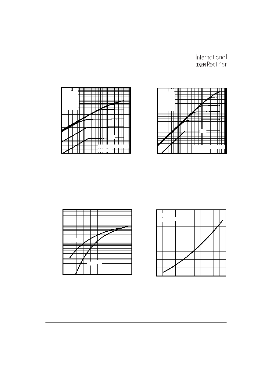
Fig 2. Typical Output Characteristics
Fig 1. Typical Output Characteristics
Fig 4. Normalized On-Resistance
Vs. Temperature
Fig 3. Typical Transfer Characteristics
0.1
1
10
100
VDS, Drain-to-Source Voltage (V)
0.01
0.1
1
10
100
1000
I D
,
D
r
a
i
n
-
t
o
-
S
o
u
r
c
e
C
u
r
r
e
n
t
(
A
)
5.0V
20µs PULSE WIDTH
Tj = 25°C
VGS
TOP 15V
10V
8.0V
7.0V
6.0V
5.5V
BOTTOM 5.0V
0.1
1
10
100
VDS, Drain-to-Source Voltage (V)
0.1
1
10
100
I D
,
D
r
a
i
n
-
t
o
-
S
o
u
r
c
e
C
u
r
r
e
n
t
(
A
)
5.0V
20µs PULSE WIDTH
Tj = 150°C
VGS
TOP 15V
10V
8.0V
7.0V
6.0V
5.5V
BOTTOM 5.0V
4.0
5.0
6.0
7.0
8.0
9.0
VGS, Gate-to-Source Voltage (V)
0
1
10
100
1000
I D
,
D
r
a
i
n
-
t
o
-
S
o
u
r
c
e
C
u
r
r
e
n
t
(
A
)
TJ = 25°C
TJ = 150°C
VDS = 50V
20µs PULSE WIDTH
-60 -40 -20
0
20
40
60
80 100 120 140 160
TJ , Junction Temperature (°C)
0.5
1.0
1.5
2.0
2.5
R
D
S
(
o
n
)
,
D
r
a
i
n
-
t
o
-
S
o
u
r
c
e
O
n
R
e
s
i
s
t
a
n
c
e
(
N
o
r
m
a
l
i
z
e
d
)
ID = 31A
VGS = 10V
Bulletin I27128 Rev.C 07/03
5
19MT050XF
www.irf.com
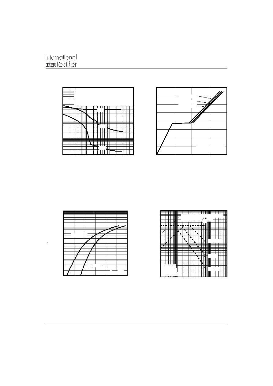
Fig 6. Typical Gate Charge Vs.
Gate-to-Source Voltage
Fig 5. Typical Capacitance Vs.
Drain-to-Source Voltage
Fig 8. Maximum Safe Operating Area
Fig 7. Typical Source-Drain Diode
Forward Voltage
1
10
100
1000
VDS, Drain-to-Source Voltage (V)
10
100
1000
10000
100000
C
,
C
a
p
a
c
i
t
a
n
c
e
(
p
F
)
Coss
Crss
Ciss
VGS = 0V, f = 1 MHZ
Ciss = Cgs + Cgd, Cds SHORTED
Crss = Cgd
Coss = Cds + Cgd
0
40
80
120
160
QG Total Gate Charge (nC)
0
4
8
12
16
V
G
S
,
G
a
t
e
-
t
o
-
S
o
u
r
c
e
V
o
l
t
a
g
e
(
V
)
VDS= 400V
VDS= 250V
VDS= 100V
ID= 31A
FOR TEST CIRCUIT
SEE FIGURE 13
0.2
0.4
0.6
0.8
1.0
1.2
1.4
VSD, Source-toDrain Voltage (V)
0.1
1.0
10.0
100.0
1000.0
I S
D
,
R
e
v
e
r
s
e
D
r
a
i
n
C
u
r
r
e
n
t
(
A
)
TJ = 25°C
TJ = 150°C
VGS = 0V
1
10
100
1000
10000
VDS , Drain-toSource Voltage (V)
0.1
1
10
100
1000
I D
,
D
r
a
i
n
-
t
o
-
S
o
u
r
c
e
C
u
r
r
e
n
t
(
A
)
Tc = 25°C
Tj = 150°C
Single Pulse
1msec
10msec
OPERATION IN THIS AREA
LIMITED BY R DS(on)
100µsec