SCHOTTKY RECTIFIER
240 Amp
240NQ... SERIES
PD-2.230 rev. B 12/97
1
www.irf.com
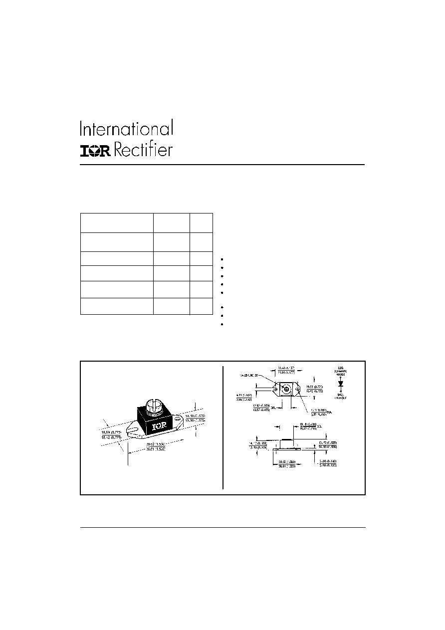
Dimensions in millimeters and inches
Outline HALF PAK Module
CASE STYLE AND DIMENSIONS
Major Ratings and Characteristics
I
F(AV)
Rectangular
240
A
waveform
V
RRM
range
35 to 45
V
I
FSM
@ tp = 5 µs sine
26,000
A
V
F
@
240Apk, T
J
=125∞C
0.55
V
T
J
range
- 55 to 150
∞C
Characteristics
240NQ...
Units
The 240NQ high current Schottky rectifier module series has
been optimized for very low forward voltage drop, with moder-
ate leakage. The proprietary barrier technology allows for
reliable operation up to 150∞ C junction temperature. Typical
applications are in switching power supplies, converters, free-
wheeling diodes, and reverse battery protection.
150∞ C T
J
operation
Unique high power, Half-Pak module
Replaces four parallel DO-5's
Easier to mount and lower profile than DO-5's
High purity, high temperature epoxy encapsulation for
enhanced mechanical strength and moisture resistance
Very low forward voltage drop
High frequency operation
Guard ring for enhanced ruggedness and long term
reliability
Description/Features
240NQ... Series
PD-2.230 rev. B 12/97
2
www.irf.com
T
J
Max. Junction Temperature Range
-55 to 150
∞C
T
stg
Max. Storage Temperature Range
-55 to 150
∞C
R
thJC
Max. Thermal Resistance Junction
0.20
∞C/W
DC operation * See Fig. 4
to Case
R
thCS
Typical Thermal Resistance, Case to
0.15
∞C/W
Mounting surface , smooth and greased
Heatsink
wt
Approximate Weight
25.6 (0.9) g (oz.)
T
Mounting Torque
Min.
40 (35)
Non-lubricated threads
Max.
58 (50)
Terminal Torque
Min.
58 (50)
Max.
86 (75)
Case Style
HALF PAK Module
Thermal-Mechanical Specifications
Parameters
240NQ Units
Conditions
Kg-cm
(Ibf-in)
V
FM
Max. Forward Voltage Drop (1)
0.61
V
@ 240A
* See Fig. 1
0.81
V
@ 480A
0.55
V
@ 240A
0.74
V
@ 480A
I
RM
Max. Reverse Leakage Current (1)
20
mA
T
J
= 25 ∞C
* See Fig. 2
800
mA
T
J
= 125 ∞C
C
T
Max. Junction Capacitance
10,300
pF
V
R
= 5V
DC
, (test signal range 100Khz to 1Mhz) 25 ∞C
L
S
Typical Series Inductance
5.0
nH
From top of terminal hole to mounting plane
dv/dt Max. Voltage Rate of Change
10,000
V/ µs
(Rated V
R
)
T
J
= 25 ∞C
T
J
= 125 ∞C
V
R
= rated V
R
Parameters
240NQ Units
Conditions
(1) Pulse Width < 300µs, Duty Cycle < 2%
Electrical Specifications
I
F(AV)
Max. Average Forward Current
240
A
50% duty cycle @ T
C
= 96∞ C, rectangular wave form
* See Fig. 5
I
FSM
Max. Peak One Cycle Non-Repetitive
26,000
5µs Sine or 3µs Rect. pulse
Surge Current * See Fig. 7
3400
10ms Sine or 6ms Rect. pulse
E
AS
Non-Repetitive Avalanche Energy
324
mJ
T
J
= 25 ∞C, I
AS
= 48 Amps, L = 0.28 mH
I
AR
Repetitive Avalanche Current
48
A
Current decaying linearly to zero in 1 µsec
Frequency limited by T
J
max. V
A
= 1.5 x V
R
typical
Parameters
240NQ Units
Conditions
Absolute Maximum Ratings
A
Following any rated
load condition and
with rated V
RRM
applied
Part number
240NQ035
240NQ040
240NQ045
V
R
Max. DC Reverse Voltage (V)
V
RWM
Max. Working Peak Reverse Voltage (V)
35
40
45
Voltage Ratings
240NQ... Series
PD-2.230 rev. B 12/97
3
www.irf.com
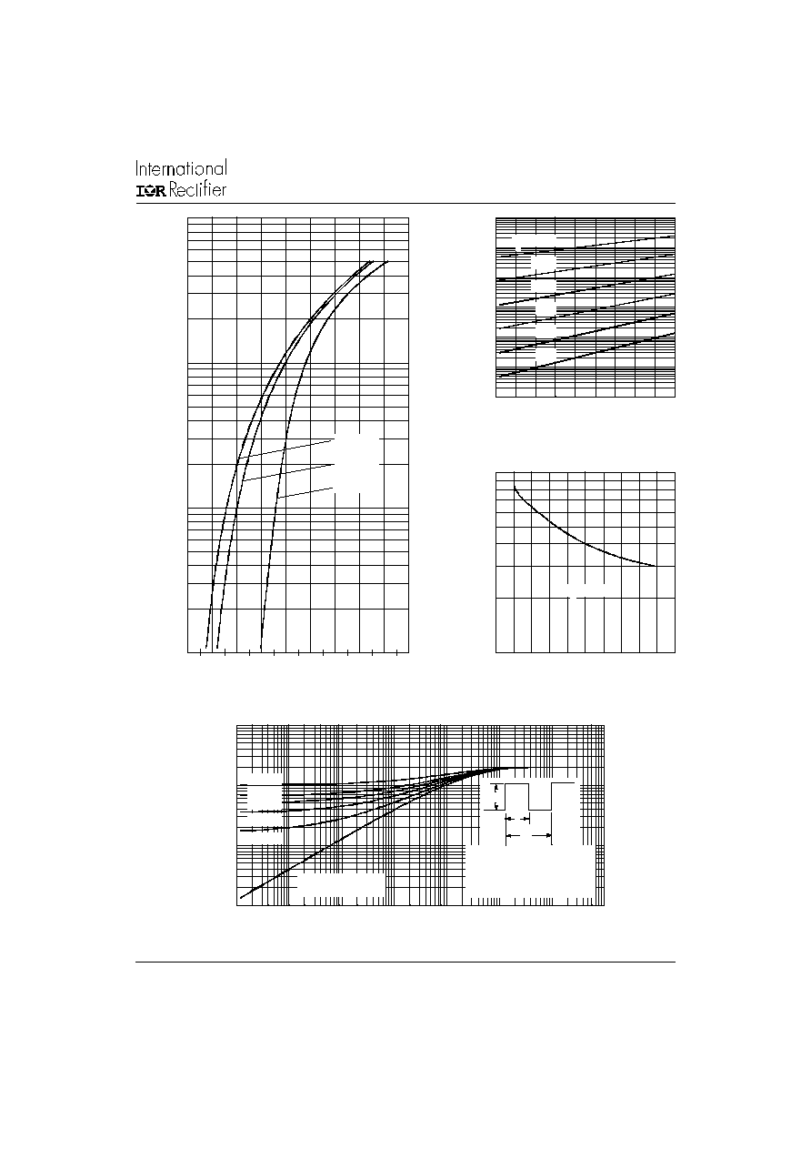
Fig. 2 - Typical Values of Reverse Current
Vs. Reverse Voltage
Fig. 3 - Typical Junction Capacitance
Vs. Reverse Voltage
Fig. 4 - Maximum Thermal Impedance Z
thJC
Characteristics
.01
.1
1
10
100
1000
10000
0
5
10 15 20 25 30 35 40 45
R
R
125∞C
100∞C
75∞C
50∞C
25∞C
Reverse Voltage - V (V)
Re
v
e
r
s
e
C
ur
r
e
nt
-
I
(
m
A)
T = 150∞C
J
1000
10000
0
10
20
30
40
50
T = 25∞C
J
Reverse Voltage - V (V)
R
T
J
u
nc
t
i
on
C
a
pa
c
i
t
a
nc
e -
C
(
p
F
)
.001
.01
.1
1
.00001
.0001
.001
.01
.1
1
10
100
D = 0.33
D = 0.50
D = 0.25
D = 0.17
D = 0.08
1
th
J
C
t , Rectangular Pulse Duration (Seconds)
Th
e
r
m
al
I
m
ped
an
c
e
-
Z
(
∞C
/
W
)
Single Pulse
(Thermal Resistance)
2
t
1
t
P
DM
Notes:
1. Duty factor D = t / t
2. Peak T = P x Z + T
1
J
DM
thJC
C
2
Fig. 1 - Maximum Forward Voltage Drop Characteristics
1
10
100
1000
0
.1
.2
.3
.4
.5
.6
.7
.8
.9
FM
F
I
n
s
t
ant
a
neo
us
F
o
r
w
a
r
d
C
u
rre
n
t
-
I
(A
)
Forward Voltage Drop - V (V)
T = 150∞C
T = 125∞C
T = 25∞C
J
J
J
240NQ... Series
PD-2.230 rev. B 12/97
4
www.irf.com
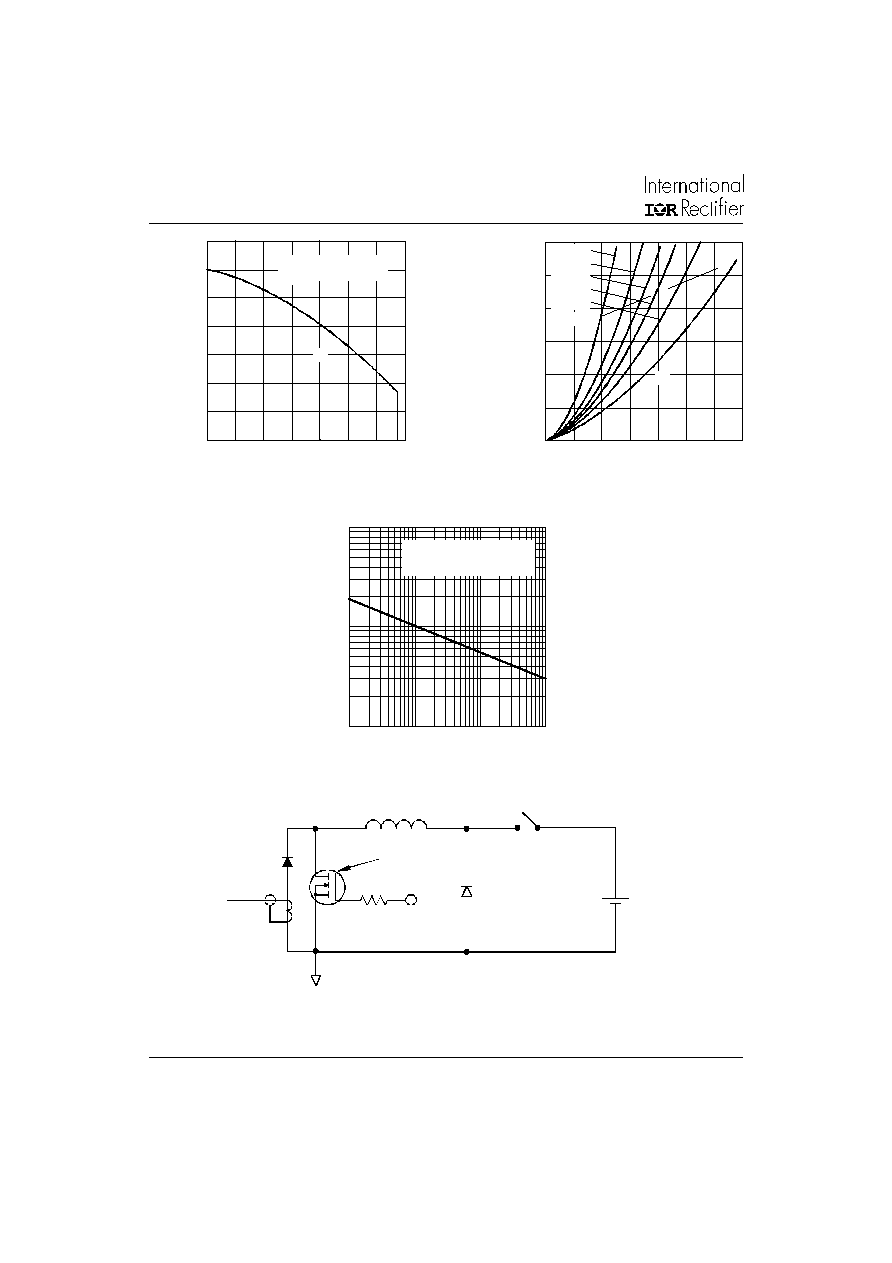
Fig. 8 - Unclamped Inductive Test Circuit
Fig. 5 - Maximum Allowable Case Temperature
Vs. Average Forward Current
Fig. 6 - Forward Power Loss Characteristics
Fig. 7 - Maximum Non-Repetitive Surge Current
0
40
80
120
160
200
240
0
50
100 150 200 250 300 350
DC
A
v
er
ag
e P
o
w
e
r
Lo
s
s
-
(
W
a
tts
)
F(AV)
D = 0.08
D = 0.17
D = 0.25
D = 0.33
D = 0.50
RMS Limit
Average Forward Current - I (A)
90
100
110
120
130
140
150
160
0
50
100 150 200 250 300 350
DC
A
l
l
o
wa
b
l
e
Ca
s
e
T
e
m
p
e
ra
t
u
re
-
(
∞C
)
Average Forward Current - I (A)
F(AV)
240NQ
R (DC) = 0.20∞C/W
thJC
1000
10000
100000
10
100
1000
10000
FS
M
p
N
on-
R
epet
i
t
i
v
e S
u
r
ge C
u
r
r
ent
-
I
(
A
)
At Any Rated Load Condition
And With Rated V Applied
Following Surge
RRM
Square Wave Pulse Duration - t (microsec)
FREE-WHEEL
DIODE
40HFL40S02
CURRENT
MONITOR
HIGH-SPEED
SWITCH
IRFP460
L
DUT
Rg = 25 ohm
Vd = 25 Volt
+