SCHOTTKY RECTIFIER
30 Amp, 150V
30CLJQ150
The 30CLJQ150 center tap Schottky rectifier has been
expressly designed to meet the rigorous requirements of hi-
rel environments. It is packaged in the hermetic surface
mount SMD-0.5 ceramic package. The device's forward
voltage drop and reverse leakage current are optimized
for the lowest power loss and the highest circuit efficiency
for typical high frequency switching power supplies and
resonent power converters. Full MIL-PRF-19500 quality
conformance testing is available on source control
drawings to TX, TXV and S quality levels.
∑ Hermetically Sealed
∑ Center Tap
∑ Low Forward Voltage Drop
∑ High Frequency Operation
∑ Guard Ring for Enhanced Ruggedness and Long term
Reliability
∑ Surface Mount
∑ Lightweight
Major Ratings and Characteristics
Description/Features
9/22/00
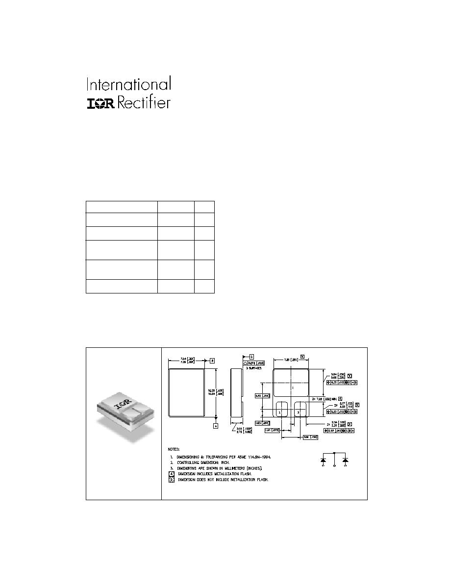
CASE STYLE
IR Case Style SMD-0.5
www.irf.com
1
Characteristics
30CLJQ150 Units
I
F(AV)
30
A
V
RRM
(Per Leg)
150
V
I
FSM
@ tp = 8.3ms half-sine
(Per Leg)
130
A
V
F
@ 15Apk, T
J
=125∞C
0.85
V
(Per Leg)
T
J
, T
stg
Operating and storage
-55 to 150
∞C
ANODE COMMON ANODE
CATHODE
2
1
3
HIGH EFFICIENCY SERIES
PD -93950B

30CLJQ150
2
www.irf.com
Part number
30CLJQ150
V
R
Max. DC Reverse Voltage (V) (Per Leg)
V
RWM
Max. Working Peak Reverse Voltage (V) (Per Leg)
Voltage Ratings
150
Parameters
Limits Units
Conditions
I
F(AV)
Max. Average Forward Current
30
A
50% duty cycle @ T
C
= 72∞C, square waveform
See Fig. 5
I
FSM
Max. Peak One Cycle Non - Repetitive
130
A
@ t
p
= 8.3 ms half-sine
Surge Current (Per Leg)
Absolute Maximum Ratings
Parameters
Limits
Units
Conditions
V
FM
Max. Forward Voltage Drop
1.06
V
@ 7.5A
T
J
= -55∞C
(Per Leg) See Fig. 1
1.23
V
@ 15A
1.05
V
@ 7.5A
T
J
= 25∞C
1.20
V
@ 15A
0.72
V
@ 7.5A
T
J
= 125∞C
0.85
V
@ 15A
I
RM
Max. Reverse Leakage Current
0.02
mA
T
J
= 25∞C
(Per Leg) See Fig. 2
2.0
mA
T
J
= 100∞C
V
R
= rated V
R
7.0
mA
T
J
= 125∞C
C
T
Max. Junction Capacitance (Per Leg)
130
pF
V
R
= 5V
DC
( 1MHz, 25∞C )
L
S
Typical Series Inductance (Per Leg)
4.8
nH
Measured from center of cathode pad to center of
anode pad
Electrical Specifications
Pulse Width < 300µs, Duty Cycle < 2%
Parameters
Limits
Units
Conditions
T
J
Max.Junction Temperature Range
-55 to 150
∞C
T
stg
Max. Storage Temperature Range
-55 to 150
∞C
R
thJC
Max. Thermal Resistance, Junction
3.5
∞C/W
DC operation
See Fig. 4
to Case (Per Leg)
R
thJC
Max. Thermal Resistance, Junction
1.75
∞C/W
DC operation
to Case (Per Package)
wt
Weight (Typical)
1.0 g
Die Size (Typical)
70X92 mils
Thermal-Mechanical Specifications
Case Style
SMD-0.5
30CLJQ150
www.irf.com
3
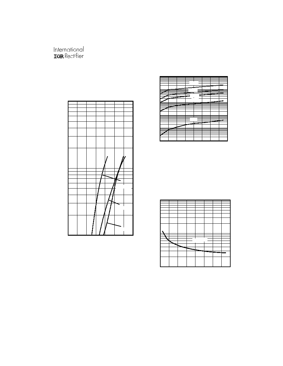
Fig. 2 - Typical Values of Reverse Current
Vs. Reverse Voltage (Per Leg)
Fig. 3 - Typical Junction Capacitance Vs.
Reverse Voltage (Per Leg)
Fig. 1 - Max. Forward Voltage Drop Characteristics
(Per Leg)
0
20
40
60
80
100
120
140
160
Reverse Voltage - VR (V)
0.0001
0.001
0.01
0.1
1
10
Reverse Current - I
R
( mA )
125∞C
110∞C
75∞C
25∞C
100∞C
0
20
40
60
80
100
120
140
160
Reverse Voltage -VR (V)
10
100
1000
Junction Capacitance - C
T
(pF)
TJ = 25∞C
0.0
0.2
0.4
0.6
0.8
1.0
1.2
1.4
Forward Voltage Drop - V F (V)
1
10
100
Instantaneous Forward Current - I
F
(A)
Tj = -55∞C
Tj = 125∞C
Tj = 25∞C
30CLJQ150
4
www.irf.com
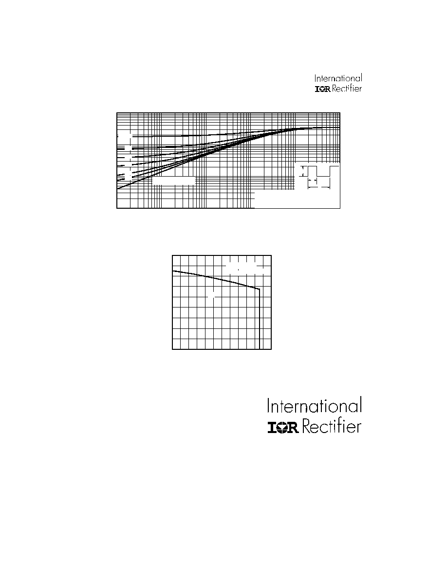
Fig. 5 - Max. Allowable Case Temperature Vs.
Average Forward Current (Per Leg)
IR WORLD HEADQUARTERS: 233 Kansas St., El Segundo, California 90245, USA Tel: (310) 252-7105
IR EUROPEAN REGIONAL CENTRE: 439/445 Godstone Rd, Whyteleafe, Surrey CR3 OBL, UK Tel: ++ 44 (0)20 8645 8000
IR CANADA: 15 Lincoln Court, Brampton, Ontario L6T3Z2, Tel: (905) 453 2200
IR GERMANY: Saalburgstrasse 157, 61350 Bad Homburg Tel: ++ 49 (0) 6172 96590
IR ITALY: Via Liguria 49, 10071 Borgaro, Torino Tel: ++ 39 011 451 0111
IR JAPAN: K&H Bldg., 2F, 30-4 Nishi-Ikebukuro 3-Chome, Toshima-Ku, Tokyo 171 Tel: 81 (0)3 3983 0086
IR SOUTHEAST ASIA: 1 Kim Seng Promenade, Great World City West Tower, 13-11, Singapore 237994 Tel: ++ 65 (0)838 4630
IR TAIWAN:16 Fl. Suite D. 207, Sec. 2, Tun Haw South Road, Taipei, 10673 Tel: 886-(0)2 2377 9936
Data and specifications subject to change without notice. 9/00
TBD
0.01
0.1
1
10
0.00001
0.0001
0.001
0.01
0.1
1
Notes:
1. Duty factor D = t / t
2. Peak T = P
x Z
+ T
1
2
J
DM
thJC
C
P
t
t
DM
1
2
t , Rectangular Pulse Duration (sec)
Thermal Response
(Z )
1
thJC
0.01
0.02
0.05
0.10
0.20
D = 0.50
SINGLE PULSE
(THERMAL RESPONSE)
Fig. 4 - Max. Thermal Impedance Z
thJC
Characteristics (Per Leg)
0
4
8
12
16
20
24
Average Forward Current - I F(AV) (A)
0
20
40
60
80
100
120
140
160
180
Allowable Case Temprature - (∞C)
30CLJQ150
R thJC = 3.5 ∞C/W
DC