 | –≠–ª–µ–∫—Ç—Ä–æ–Ω–Ω—ã–π –∫–æ–º–ø–æ–Ω–µ–Ω—Ç: 40L15CT-1 | –°–∫–∞—á–∞—Ç—å:  PDF PDF  ZIP ZIP |

SCHOTTKY RECTIFIER
2 x 20 Amps
40L15CT
40L15CTS
40L15CT-1
Bulletin PD-20568 rev. E 09/01
1
www.irf.com
I
F(AV)
Rectangular
40
A
waveform
V
RRM
15
V
I
FSM
@ tp = 5 µs sine
700
A
V
F
@
19 Apk, T
J
=125∞C
0.25
V
(per leg, Typical)
T
J
- 55 to 125
∞C
Characteristics
Values
Units
Major Ratings and Characteristics
Description/Features
The center tap Schottky rectifier module has been optimized for
ultra low forward voltage drop specifically for the OR-ing of
parallel power supplies. The proprietary barrier technology
allows for reliable operation up to 125 ∞C junction temperature.
Typical applications are in parallel switching power supplies,
converters, reverse battery protection, and redundant power
subsystems.
125∞C T
J
operation (V
R
< 5V)
Center tap module
Optimized for OR-ing applications
Ultra low forward voltage drop
High frequency operation
Guard ring for enhanced ruggedness and long term
reliability
High purity, high temperature epoxy encapsulation for
enhanced mechanical strength and moisture resistance
40L15CT
TO-220AB
Case Styles
40L15CTS
D
2
PAK
40L15CT-1
TO-262
Anode
1
3
2
Base
Common
Cathode
2
Anode
Common
Cathode
Anode
1
3
2
Base
Common
Cathode
2
Anode
Common
Cathode
Anode
1
3
2
Base
Common
Cathode
2
Anode
Common
Cathode

40L15CT, 40L15CTS, 40L15CT-1
Bulletin PD-20568 rev. E 09/01
2
www.irf.com
Part number
Values
V
R
Max. DC Reverse Voltage (V)
@ T
J
= 100 ∞C
V
RWM
Max. Working Peak Reverse Voltage (V) @ T
J
= 100 ∞C
15
T
J
Max. Junction Temperature Range
-55 to 125
∞C
T
stg
Max. Storage Temperature Range
-55 to 150
∞C
R
thJC
Max. Thermal Resistance
1.5
∞C/W DC operation
* See Fig. 4
Junction to Case
(Per Leg)
R
thCS
Typical Thermal Resistance
0.50
∞C/W Mounting surface , smooth and greased
Case to Heatsink
Only for TO-220
R
thJA
Max. Thermal Resistance
40
∞C/W DC operation
Junction to Ambient
For D
2
Pak and TO-262
wt
Approximate Weight
2 (0.07)
g (oz.)
T
Mounting Torque
Min.
6 (5)
Non-lubricated threads
Max.
12 (10)
Thermal-Mechanical Specifications
Kg-cm
(Ibf-in)
Parameters
Values
Units
Conditions
Absolute Maximum Ratings
Following any rated
load condition and with
rated V
RRM
applied
Parameters
Values
Units
Conditions
A
Typ. Max.
V
FM
Forward Voltage Drop
-
0.41
V
@ 19A
(Per Leg) * See Fig. 1
(1)
-
0.52
V
@ 40A
0.25 0.33
V
@ 19A
0.37 0.50
V
@ 40A
I
RM
Reverse Leakage Current
-
10
mA
T
J
= 25 ∞C
(Per Leg) * See Fig. 2
(1)
-
600
mA
T
J
= 100 ∞C
V
F(TO)
Threshold Voltage
0.182
V
T
J
=
T
J
max.
r
t
Forward Slope Resistance
7.6
m
C
T
Max. Junction Capacitance (Per Leg)
-
2000
pF
V
R
= 5V
DC
, (test signal range 100Khz to 1Mhz) 25∞C
L
S
Typical Series Inductance (Per Leg)
8
-
nH
Measured lead to lead 5mm from package body
dv/dt Max. Voltage Rate of Change
10,000
V/ µs
(Rated V
R
)
T
J
= 25 ∞C
T
J
= 125 ∞C
V
R
= rated V
R
Parameters
Values
Units
Conditions
(1) Pulse Width < 300µs, Duty Cycle <2%
Voltage Ratings
Electrical Specifications
I
F(AV)
Max. Average Forward
(Per Leg)
20
A
50% duty cycle @ T
C
= 85∞C, rectangular wave form
Current * See Fig. 5
(Per Device)
40
I
FSM
Max. Peak One Cycle Non-Repetitive
700
5µs Sine or 3µs Rect. pulse
Surge Current (Per Leg) * See Fig. 7
330
10ms Sine or 6ms Rect. pulse
E
AS
Non-Repetitive Avalanche Energy
10
mJ
T
J
= 25 ∞C, I
AS
= 2 Amps, L = 6 mH
(Per Leg)
I
AR
Repetitive Avalanche Current
2
A
Current decaying linearly to zero in 1 µsec
(Per Leg)
Frequency limited by T
J
max. V
A
= 1.5 x V
R
typical
40L15CT, 40L15CTS, 40L15CT-1
Bulletin PD-20568 rev. E 09/01
3
www.irf.com
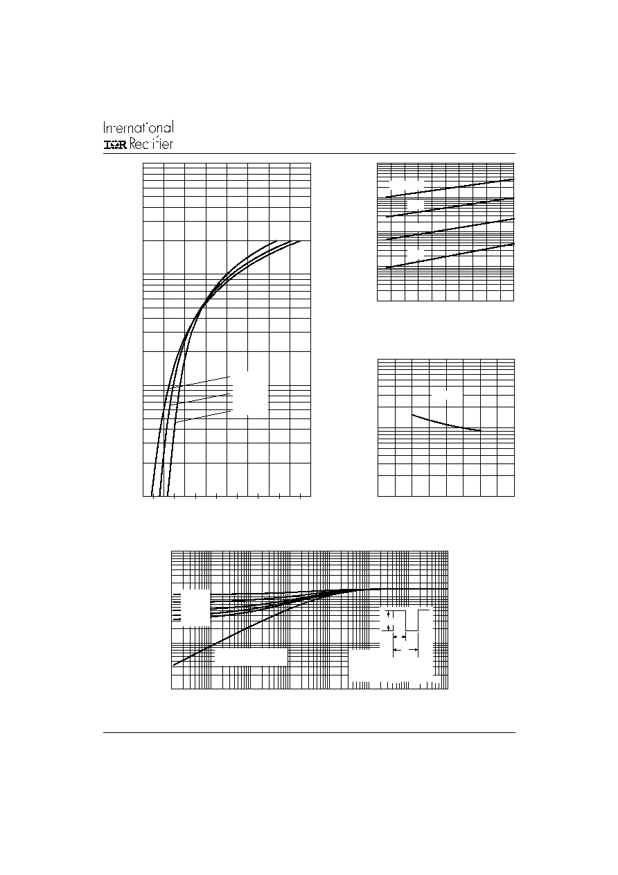
Fig. 2 - Typical Values of Reverse Current
Vs. Reverse Voltage
Fig. 3 - Typical Junction Capacitance
Vs. Reverse Voltage
Fig. 4 - Maximum Thermal Impedance Z
thJC
Characteristics
Fig. 1 - Maximum Forward Voltage Drop Characteristics
1
1 0
1 0 0
1 00 0
0
0 .2
0 .4
0.6
0.8
1
1 .2
1.4
1 .6
F
FM
Forw a rd V olta g e D rop - V (V )
I
n
s
t
an
t
a
n
e
o
u
s
F
o
r
w
ar
d
C
u
r
r
e
n
t
-
I
(
A
)
T = 12 5 C
T = 7 5 C
T = 2 5 C
J
J
J
0 .1
1
10
1 0 0
10 0 0
0
3
6
9
12
15
R
R
75 C
50 C
25 C
Re
v
e
r
s
e C
u
r
r
e
n
t
-
I
(
m
A
)
Re ve rse V oltag e - V (V )
T = 100 C
J
1 0 0
1 0 00
1 00 0 0
0
5
10
1 5
2 0
R
T
J
u
n
c
ti
o
n
C
a
p
a
c
i
ta
n
c
e
-
C
(
p
F
)
Re ve rse V olta g e - V (V )
T = 2 5 C
J
0 .0 1
0 .1
1
10
0.00 00 1
0 .00 0 1
0 .0 01
0.0 1
0 .1
1
10
100
th
J
C
t , R e c tan g ular Pu lse D ura tio n (Sec o nd s)
Sin gle Pu lse
(Therm a l R esista n c e)
1
Th
e
r
m
a
l
I
m
p
e
d
a
n
c
e
Z
(
C
/
W
)
N otes:
1. D uty fac tor D = t / t
2. Pe ak T = P x Z + T
1
2
J
thJ C
C
D M
D = 0 .75
D = 0 .50
D = 0 .33
D = 0 .25
D = 0 .2 0
2
t
1
t
P
D M
40L15CT, 40L15CTS, 40L15CT-1
Bulletin PD-20568 rev. E 09/01
4
www.irf.com
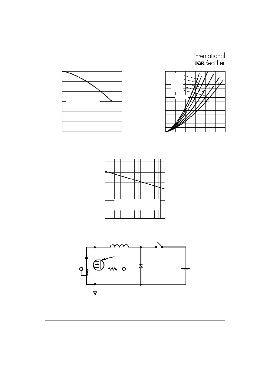
Fig. 8 - Unclamped Inductive Test Circuit
Fig. 5 - Maximum Allowable Case Temperature
Vs. Average Forward Current
Fig. 6 - Forward Power Loss Characteristics
Fig. 7 - Maximum Non-Repetitive Surge Current
FR EE-W HE EL
D IO D E
40H FL40S02
C UR RE N T
M O N ITO R
H IG H -SPE ED
SW ITC H
IRFP460
L
D UT
Rg = 25 ohm
V d = 25 V olt
+
0
2
4
6
8
10
12
14
0
5
10
15
2 0
2 5
3 0
D C
A
v
e
r
ag
e
P
o
w
e
r
L
o
s
s
-
(
W
at
t
s
)
F(A V)
RM S Lim it
D = 0.20
D = 0.25
D = 0.33
D = 0.50
D = 0.75
A ve ra g e Forw a rd C urre n t - I (A)
100
1000
10
100
1000
10000
FS
M
N
o
n
-
R
e
p
e
ti
ti
v
e
S
u
r
g
e
C
u
r
r
e
n
t -
I
(
A
)
p
A t A n y Rate d Load C on d ition
A n d W ith Rate d V Ap plie d
Follow in g Surg e
RRM
Sq uare W ave Pulse D uration - t (m ic rose c )
7 0
7 5
8 0
8 5
9 0
9 5
1 00
0
4
8
1 2
16
20
24
A
l
l
o
w
a
b
l
e C
a
s
e
T
e
m
p
e
r
a
t
u
r
e -
(
C
)
F(A V)
se e n o te ( 2)
A ve ra g e Forw ard C urren t - I (A)
Squa re w ave (D = 0.50)
(2) Formula used: T
C
= T
J
- (Pd + Pd
REV
) x R
thJC
;
Pd = Forward Power Loss = I
F(AV)
x V
FM
@ (I
F(AV)
/
D) (see Fig. 6);
Pd
REV
= Inverse Power Loss = V
R1
x I
R
(1 - D); I
R
@ V
R1
= 80% rated V
R

40L15CT, 40L15CTS, 40L15CT-1
Bulletin PD-20568 rev. E 09/01
5
www.irf.com
Outline Table
3.78 (0.15)
3.54 (0.14)
10.54 (0.41)
MAX.
DIA.
15.24 (0.60)
14.84 (0.58)
2.92 (0.11)
2.54 (0.10)
1
TERM 2
14.09 (0.55)
13.47 (0.53)
3.96 (0.16)
3.55 (0.14)
0.94 (0.04)
0.69 (0.03)
4.57 (0.18)
4.32 (0.17)
3
0.61 (0.02) MAX.
5.08 (0.20) REF.
1.32 (0.05)
1.22 (0.05)
6.48 (0.25)
6.23 (0.24)
2∞
0.10 (0.004)
1.40 (0.05)
1.15 (0.04)
2.89 (0.11)
2.64 (0.10)
1
3
2.04 (0.080) MAX.
2
2
Conform to JEDEC outline TO-220AB
Dimensions in millimeters and (inches)
10.16 (0.40)
REF.
8.89 (0.35)
4.57 (0.18)
4.32 (0.17)
0.61 (0.02) MAX.
5.08 (0.20) REF.
1.32 (0.05)
1.22 (0.05)
1
3
6.47 (0.25)
6.18 (0.24)
93∞
REF.
2.61 (0.10)
2.32 (0.09)
5.28 (0.21)
4.78 (0.19)
4.69 (0.18)
4.20 (0.16)
0.55 (0.02)
0.46 (0.02)
14.73 (0.58)
15.49 (0.61)
1.40 (0.055)
1.14 (0.045)
3X
0.93 (0.37)
0.69 (0.27)
2X
11.43 (0.45)
17.78 (0.70)
8.89 (0.35)
3.81 (0.15)
2.08 (0.08)
2X
2.54 (0.10)
2X
MINIMUM RECOMMENDED FOOTPRINT
2
Conform to JEDEC outline D
2
Pak (SMD-220)
Dimensions in millimeters and (inches)
Anode
1
3
2
Base
Common
Cathode
2
Anode
Common
Cathode
Anode
1
3
2
Base
Common
Cathode
2
Anode
Common
Cathode