 | –≠–ª–µ–∫—Ç—Ä–æ–Ω–Ω—ã–π –∫–æ–º–ø–æ–Ω–µ–Ω—Ç: 70CRU04 | –°–∫–∞—á–∞—Ç—å:  PDF PDF  ZIP ZIP |
1
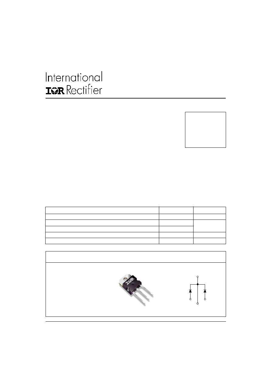
Case Styles
70CRU04
Bulletin PD-20637 12/01
t
rr
= 38ns
I
F(AV)
= 70Amp
@T
C
= 116∞C
V
R
= 400V
Features
Description/ Applications
Absolute Maximum Ratings
Ultrafast Rectifier
V
R
Cathode to Anode Voltage
400
V
I
F(AV)
Continuous Forward Current
T
C
= 116∞C
Per Diode
35
A
I
FSM
Single Pulse Forward Current
T
C
= 25∞C
Per Diode
300
P
D
Maximum Power Dissipation
T
C
= 100∞C
Per Module
47
W
T
J
,
T
STG
Operating Junction and Storage Temperatures
- 55 to 175
∞C
Parameters
Max
Units
∑ Two Common-Cathode Diodes
∑ Ultrafast Reverse Recovery
∑ Ultrasoft Reverse Recovery Current Shape
∑ Low Forward Voltage Drop
∑ Low Leakage Current
∑ Optimized for Power Conversion: Welding and Industrial SMPS Applications
∑ Up to 175∞C Operating Junction Temperature
The 70CRU04 integrates two state-of-the-art International Rectifier's Ultrafast recovery rectifiers in the common-
cathode configuration. The planar structure of the diodes, and the platinum doping life-time control, provide a
Ultrasoft recovery current shape, together with the best overall performance, ruggedness and reliability
characteristics.
These devices are thus intended for high frequency applications in which the switching energy is designed not to be
predominant portion of the total energy, such as in the output rectification stage of Welding machines, SMPS, DC-
DC converters. Their extremely optimized stored charge and low recovery current reduce both over-dissipation in
the switching elements (and snubbers) and EMI/RFI.
70CRU04
TO-218
www.irf.com
Base
Common
Cathode
Anode
Anode
Common
Cathode
1
3
2
1
2
2
70CRU04
Bulletin PD-20637 12/01
2
www.irf.com
V
BR
,
V
r
Breakdown Voltage,
400
-
-
V
I
R
= 100µA
Blocking Voltage
V
F
Forward Voltage
-
1.11 1.32
V
I
F
= 35A
-
0.98 1.14
V
I
F
= 35A, T
J
= 125∞C
-
0.92 1.05
V
I
F
= 35A, T
J
= 175∞C
I
R
Reverse Leakage Current
-
-
100
µA
V
R
= V
R
Rated
-
-
2
mA
T
J
= 150∞C, V
R
= V
R
Rated
C
T
Junction Capacitance
-
70
-
pF
V
R
= 400V
Electrical Characteristics per Diode @ T
J
= 25∞C (unless otherwise specified)
Parameters
Min Typ Max Units Test Conditions
t
rr
Reverse Recovery Time
-
32
38
ns
T
J
= 25∞C
t
rr
Reverse Recovery Time
-
72
-
ns
T
J
= 25∞C
-
130
-
T
J
= 125∞C
I
RRM
Peak Recovery Current
-
7.7
-
A
T
J
= 25∞C
-
16.5
-
T
J
= 125∞C
Q
rr
Reverse Recovery Charge
-
0.28
-
µC
T
J
= 25∞C
-
1.08
-
T
J
= 125∞C
Dynamic Recovery Characteristics per Diode @ T
J
= 25∞C (unless otherwise specified)
I
F
= 1A
V
R
= 30V
di
F
/dt = 200A/µs
Parameters
Min Typ Max Units Test Conditions
Thermal - Mechanical Characteristics
Parameters
Min
Typ
Max
Units
R
thJC
Thermal Resistance, Junction to Case
Per Diode
-
0.8
1.6
K/W
R
thJC
Thermal Resistance, Junction to Case
Both Diodes
-
0.4
0.8
R
thCS
(1)
Thermal Resistance, Case to Heatsink
-
0.2
-
Wt
Weight
-
4
-
g
-
0.13
-
(oz)
T
Mounting Torque
1.2
-
2.4
N * m
10
-
20
lbf.in
!
(1) Mounting Surface, Flat, Smooth and Greased
I
F
= 35A
V
R
= 200V
di
F
/dt = 200A/µs
Bulletin PD-20637 12/01
3
70CRU04
www.irf.com
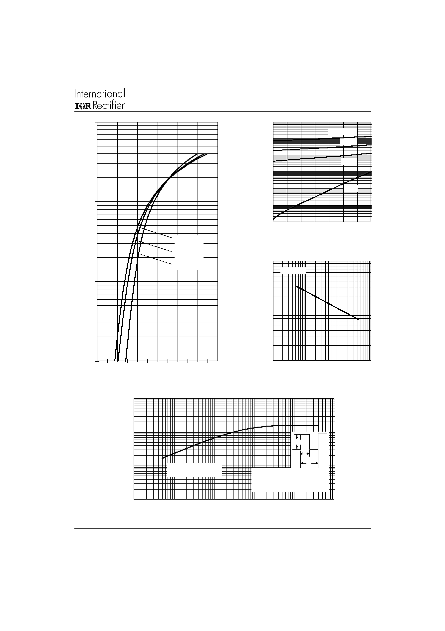
Fig. 1 - Typical Forward Voltage Drop Characteristics
(Per Diode)
Fig. 4 - Max. Thermal Impedance Z
thJC
Characteristics (Per Diode)
Forward Voltage Drop - V
FM
(V)
Instantaneous Forward Current - I
F
(A)
Reverse Voltage - V
R
(V)
Reverse Voltage - V
R
(V)
Junction Capacitance - C
T
(pF)
t
1
, Rectangular Pulse Duration (Seconds)
Thermal Impedance Z
thJC
(∞C/W)
Fig. 3 - Typical Junction Capacitance
Vs. Reverse Voltage
Reverse Current - I
R
(µA)
Fig. 2 - Typical Values Of Reverse Current
Vs. Reverse Voltage
10
100
1000
1
10
100
1000
Tj = 25∞C
1
10
100
1000
0
0.5
1
1.5
2
2.5
3
Tj = 175∞C
Tj = 125∞C
Tj = 25∞C
0.01
0.1
1
10
0.0001
0.001
0.01
0.1
1
10
Single Pulse
(Thermal Resistance)
2
t
1
t
P
DM
Notes:
1. Duty factor D = t1/ t2
2. Peak Tj = Pdm x ZthJC + Tc
0.001
0.01
0.1
1
10
100
1000
50
100 150 200 250 300 350 400
125∞C
25∞C
150∞C
Tj = 175∞C

70CRU04
Bulletin PD-20637 12/01
4
www.irf.com
Fig. 5 - Max. Allowable Case Temperature
Vs. Average Forward Current
Fig. 8 - Typical Stored Charge vs. di
F
/dt
Fig. 6 - Forward Power Loss Characteristics
(3) Formula used: T
C
= T
J
- (Pd + Pd
REV
) x R
thJC
;
Pd = Forward Power Loss = I
F(AV)
x V
FM
@ (I
F(AV)
/
D) (see Fig. 6);
Pd
REV
= Inverse Power Loss = V
R1
x I
R
(1 - D); I
R
@ V
R1
= rated V
R
Average Forward Current - I
F(AV)
(A)
Fig. 7 - Typical Reverse Recovery vs. di
F
/dt
Allowable Case Temperature (∞C)
Average Power Loss ( Watts )
trr ( ns )
Qrr ( nC )
di
F
/dt (A/µs )
di
F
/dt (A/µs )
Average Forward Current - I
F(AV)
(A)
100
110
120
130
140
150
160
170
180
0
5
10
15
20
25
30
35
40
DC
Square wave (D = 0.50)
Rated Vr applied
see note (3)
0
5
10
15
20
25
30
35
40
0
5
10
15
20
25
30
35
RMS Limit
D = 0.01
D = 0.02
D = 0.05
D = 0.10
D = 0.20
D = 0.50
DC
50
60
70
80
90
100
110
120
130
140
150
100
1000
Tj = 125∞C
Tj = 25∞C
If = 35A
Vrr = 200V
0
500
1000
1500
2000
2500
100
1000
Tj = 125∞C
Tj = 25∞C
If = 35A
Vrr = 200V

Bulletin PD-20637 12/01
5
70CRU04
www.irf.com
Outline Table
ASSEMBLY LOT CODE
70CRU04
1043
0136
INTERNATIONAL RECTIFIER LOGO
DATE CODE (YYWW)
WW = WEEK
YY = YEAR
IR PART NUMBER
Marking Information
Dimensions in inches (and milimetres)