 | –≠–ª–µ–∫—Ç—Ä–æ–Ω–Ω—ã–π –∫–æ–º–ø–æ–Ω–µ–Ω—Ç: 7413 | –°–∫–∞—á–∞—Ç—å:  PDF PDF  ZIP ZIP |

www.irf.com
1
3/19/02
IRF7413
SMPS MOSFET
HEXFET
Æ
Power MOSFET
l
High frequency DC-DC converters
Benefits
Applications
l
Low Gate to Drain Charge to Reduce
Switching Losses
l
Fully Characterized Capacitance Including
Effective C
OSS
to Simplify Design, (See
App. Note AN1001)
l
Fully Characterized Avalanche Voltage
and Current
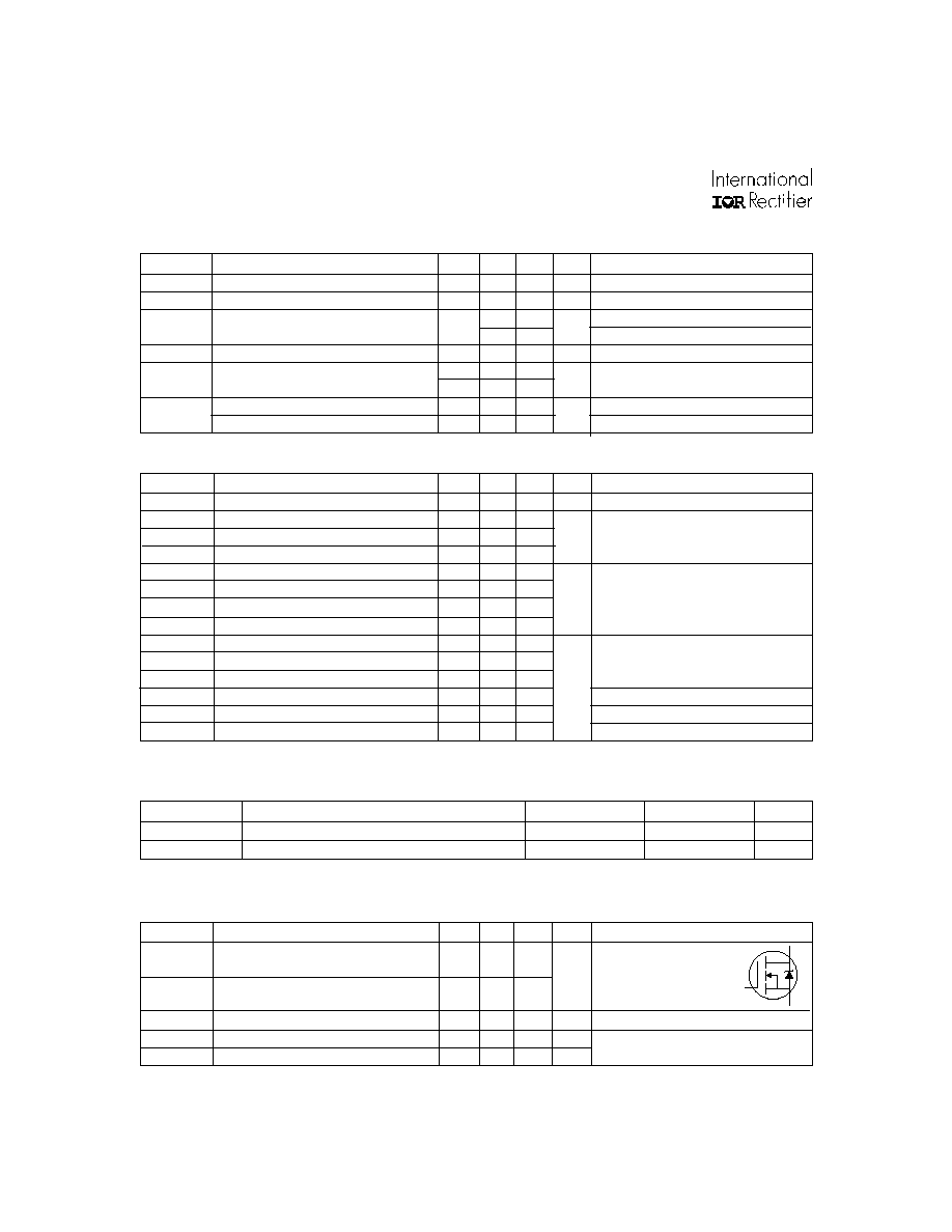
Parameter
Max.
Units
I
D
@ T
A
= 25∞C
Continuous Drain Current, V
GS
@ 10V
12
I
D
@ T
A
= 70∞C
Continuous Drain Current, V
GS
@ 10V
9.6
A
I
DM
Pulsed Drain Current
96
P
D
@T
A
= 25∞C
Power Dissipation
2.5
W
Linear Derating Factor
0.02
W/∞C
V
GS
Gate-to-Source Voltage
± 20
V
dv/dt
Peak Diode Recovery dv/dt
1.0
V/ns
T
J
Operating Junction and
-55 to + 150
T
STG
Storage Temperature Range
Soldering Temperature, for 10 seconds
300 (1.6mm from case )
∞C
Absolute Maximum Ratings
Notes
through
are on page 8
SO-8
Top View
8
1
2
3
4
5
6
7
D
D
D
D
G
S
A
S
S
A
V
DSS
R
DS(on)
max(m
W)
I
D
30V
11@V
GS
= 10V
12A
Symbol
Parameter
Typ.
Max.
Units
R
JL
Junction-to-Drain Lead
≠≠≠
20
R
JA
Junction-to-Ambient
≠≠≠
50
∞C/W
Thermal Resistance
PD- 91330F
IRF7413
2
www.irf.com
Parameter
Min. Typ. Max. Units
Conditions
g
fs
Forward Transconductance
16
≠≠≠
≠≠≠
S
V
DS
= 10V, I
D
= 7.2A
Q
g
Total Gate Charge
≠≠≠
44
66 I
D
= 7.2A
Q
gs
Gate-to-Source Charge
≠≠≠
7.9
≠≠≠
nC
V
DS
= 24V
Q
gd
Gate-to-Drain ("Miller") Charge
≠≠≠
9.2
≠≠≠
V
GS
= 10V,
t
d(on)
Turn-On Delay Time
≠≠≠
8.8
≠≠≠
V
DD
= 100V
t
r
Rise Time
≠≠≠
8.0
≠≠≠
I
D
= 7.2A
t
d(off)
Turn-Off Delay Time
≠≠≠
35
≠≠≠
R
G
= 6.2
t
f
Fall Time
≠≠≠
14
≠≠≠
V
GS
= 10V
C
iss
Input Capacitance
≠≠≠
1670 ≠≠≠
V
GS
= 0V
C
oss
Output Capacitance
≠≠≠
670
≠≠≠
V
DS
= 25V
C
rss
Reverse Transfer Capacitance
≠≠≠
100
≠≠≠
pF
= 1.0MHz
C
oss
Output Capacitance
≠≠≠
2290 ≠≠≠
V
GS
= 0V, V
DS
= 1.0V, = 1.0MHz
C
oss
Output Capacitance
≠≠≠
680
≠≠≠
V
GS
= 0V, V
DS
= 24V, = 1.0MHz
C
oss
eff.
Effective Output Capacitance
≠≠≠
1020 ≠≠≠
V
GS
= 0V, V
DS
= 0V to 24V
Dynamic @ T
J
= 25∞C (unless otherwise specified)
ns
Parameter
Typ.
Max.
Units
E
AS
Single Pulse Avalanche Energy
≠≠≠
120
mJ
I
AR
Avalanche Current
≠≠≠
7.2
A
Avalanche Characteristics
S
D
G
Parameter
Min. Typ. Max. Units
Conditions
I
S
Continuous Source Current
MOSFET symbol
(Body Diode)
≠≠≠
≠≠≠
showing the
I
SM
Pulsed Source Current
integral reverse
(Body Diode)
≠≠≠
≠≠≠
p-n junction diode.
V
SD
Diode Forward Voltage
≠≠≠
≠≠≠
1.0
V
T
J
= 25∞C, I
S
= 7.2A, V
GS
= 0V
t
rr
Reverse Recovery Time
≠≠≠
50
75
ns
T
J
= 25∞C, I
F
= 7.2A
Q
rr
Reverse RecoveryCharge
≠≠≠
74
110
nC
di/dt = 100A/µs
Diode Characteristics
3.1
96
A
Static @ T
J
= 25∞C (unless otherwise specified)
I
GSS
I
DSS
Drain-to-Source Leakage Current
R
DS(on)
Static Drain-to-Source On-Resistance
m
Symbol
Parameter
Min. Typ. Max. Units
Conditions
V
(BR)DSS
Drain-to-Source Breakdown Voltage
30
≠≠≠
≠≠≠
V
V
GS
= 0V, I
D
= 250µA
V
(BR)DSS
/
T
J
Breakdown Voltage Temp. Coefficient
≠≠≠
0.03
≠≠≠
V/∞C
Reference to 25∞C, I
D
= 1mA
≠≠≠
≠≠≠
11
V
GS
= 10V, I
D
= 7.2A
≠≠≠
≠≠≠
18
V
GS
= 4.5V, I
D
= 6.0A
V
GS(th)
Gate Threshold Voltage
1.0
≠≠≠
≠≠≠
V
V
DS
= V
GS
, I
D
= 250µA
≠≠≠
≠≠≠
1.0
µA
V
DS
= 24V, V
GS
= 0V
≠≠≠
≠≠≠
25
V
DS
= 24V, V
GS
= 0V, T
J
= 125∞C
Gate-to-Source Forward Leakage
≠≠≠
≠≠≠
100
V
GS
= 20V
Gate-to-Source Reverse Leakage
≠≠≠
≠≠≠
-100
nA
V
GS
= -20V
IRF7413
www.irf.com
3
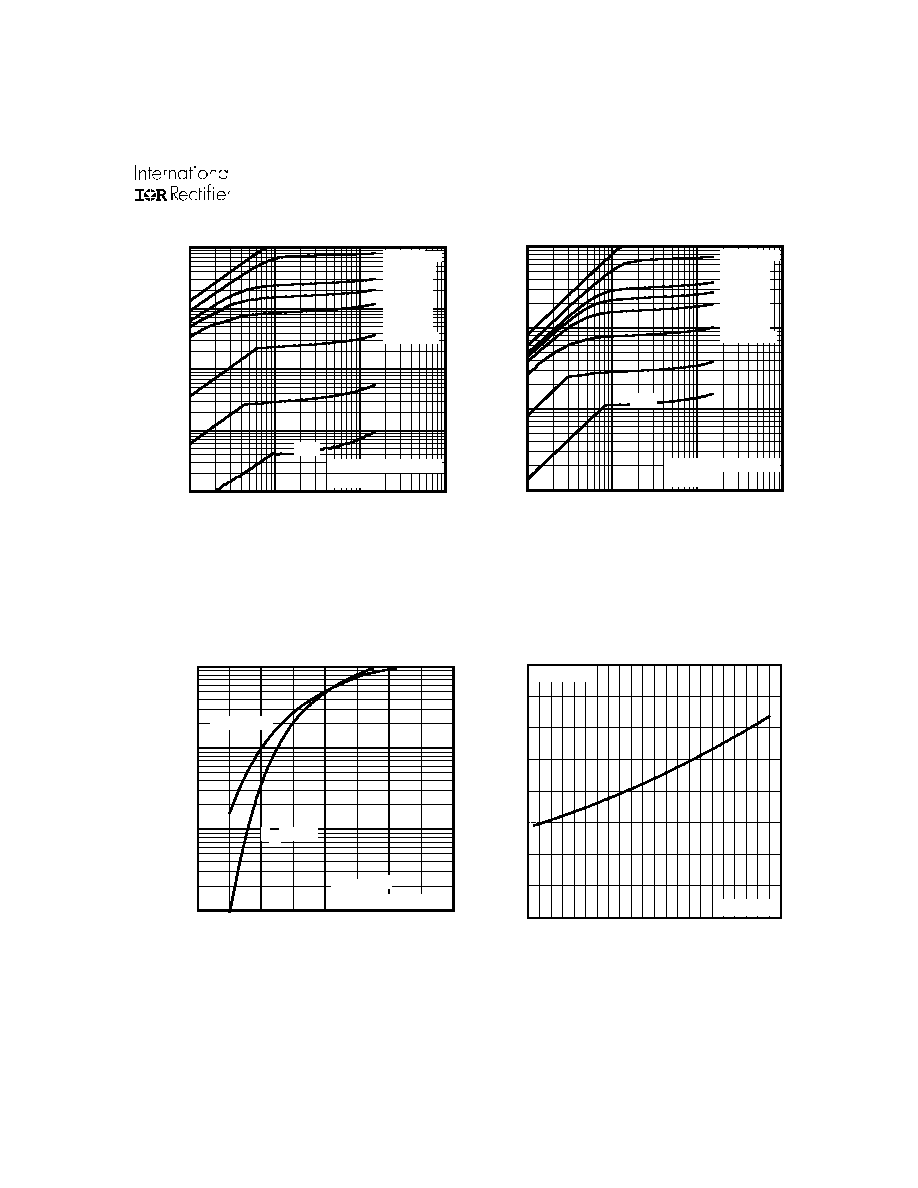
Fig 2. Typical Output Characteristics
Fig 1. Typical Output Characteristics
Fig 3. Typical Transfer Characteristics
Fig 4. Normalized On-Resistance
Vs. Temperature
-60 -40 -20
0
20
40
60
80 100 120 140 160
0.0
0.5
1.0
1.5
2.0
T , Junction Temperature ( C)
R , Drain-to-Source On Resistance
(Normalized)
J
D
S
(
on)
∞
V
=
I =
GS
D
10V
12A
0.1
1
10
100
VDS, Drain-to-Source Voltage (V)
0.01
0.1
1
10
100
I D
,
D
r
a
i
n
-
t
o
-
S
o
u
r
c
e
C
u
r
r
e
n
t
(
A
)
2.5V
20µs PULSE WIDTH
Tj = 25∞C
VGS
TOP 10V
4.5V
3.7V
3.5V
3.3V
3.0V
2.7V
BOTTOM 2.5V
0.1
1
10
100
VDS, Drain-to-Source Voltage (V)
0.1
1
10
100
I D
,
D
r
a
i
n
-
t
o
-
S
o
u
r
c
e
C
u
r
r
e
n
t
(
A
)
2.5V
20µs PULSE WIDTH
Tj = 150∞C
VGS
TOP 10V
4.5V
3.7V
3.5V
3.3V
3.0V
2.7V
BOTTOM 2.5V
2.0
3.0
4.0
5.0
6.0
VGS , Gate-to-Source Voltage (V)
0
1
10
100
I D
,
D
r
a
i
n
-
t
o
-
S
o
u
r
c
e
C
u
r
r
e
n
t
(
A
)
TJ = 25∞C
TJ = 150∞C
VDS = 15V
20µs PULSE WIDTH

IRF7413
4
www.irf.com
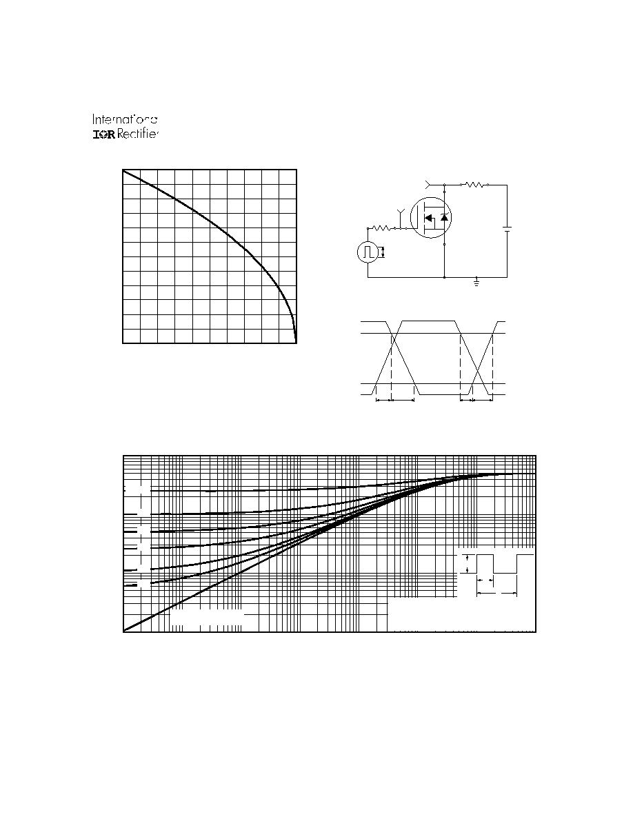
Fig 6. Typical Gate Charge Vs.
Gate-to-Source Voltage
Fig 5. Typical Capacitance Vs.
Drain-to-Source Voltage
Fig 7. Typical Source-Drain Diode
Forward Voltage
Fig 8. Maximum Safe Operating Area
1
10
100
VDS, Drain-to-Source Voltage (V)
10
100
1000
10000
100000
C
,
C
a
p
a
c
i
t
a
n
c
e
(
p
F
)
Coss
Crss
Ciss
VGS = 0V, f = 1 MHZ
C iss = C gs + C gd , C ds
SHORTED
Crss = Cgd
Coss = Cds + Cgd
0
10
20
30
40
50
QG Total Gate Charge (nC)
0
2
4
6
8
10
12
V
G
S
,
G
a
t
e
-
t
o
-
S
o
u
r
c
e
V
o
l
t
a
g
e
(
V
)
VDS= 24V
VDS= 15V
VDS= 6.0V
ID= 7.2A
0.4
0.6
0.8
1.0
1.2
VSD, Source-toDrain Voltage (V)
0.1
1.0
10.0
100.0
I S
D
,
R
e
v
e
r
s
e
D
r
a
i
n
C
u
r
r
e
n
t
(
A
)
TJ = 25∞C
TJ = 150∞C
VGS = 0V
0
1
10
100
1000
VDS , Drain-toSource Voltage (V)
1
10
100
1000
I D
,
D
r
a
i
n
-
t
o
-
S
o
u
r
c
e
C
u
r
r
e
n
t
(
A
)
Tc = 25∞C
Tj = 150∞C
Single Pulse
1msec
10msec
OPERATION IN THIS AREA
LIMITED BY R DS(on)
100µsec
IRF7413
www.irf.com
5
Fig 11. Maximum Effective Transient Thermal Impedance, Junction-to-Ambient
0.1
1
10
100
0.00001
0.0001
0.001
0.01
0.1
1
10
100
Notes:
1. Duty factor D =
t / t
2. Peak T = P
x Z
+ T
1
2
J
DM
thJA
A
P
t
t
DM
1
2
t , Rectangular Pulse Duration (sec)
Ther
m
a
l
R
e
sponse
(Z
)
1
th
J
A
0.01
0.02
0.05
0.10
0.20
D = 0.50
SINGLE PULSE
(THERMAL RESPONSE)
Fig 10a. Switching Time Test Circuit
V
DS
90%
10%
V
GS
t
d(on)
t
r
t
d(off)
t
f
Fig 10b. Switching Time Waveforms
V
DS
Pulse Width
1
µs
Duty Factor
0.1 %
R
D
V
GS
R
G
D.U.T.
10V
+
-
V
DD
25
50
75
100
125
150
0
2
4
6
8
10
12
T , Case Temperature
( C)
I , Drain Current (A)
∞
C
D
Fig 9. Maximum Drain Current Vs.
Ambient Temperature
IRF7413
6
www.irf.com
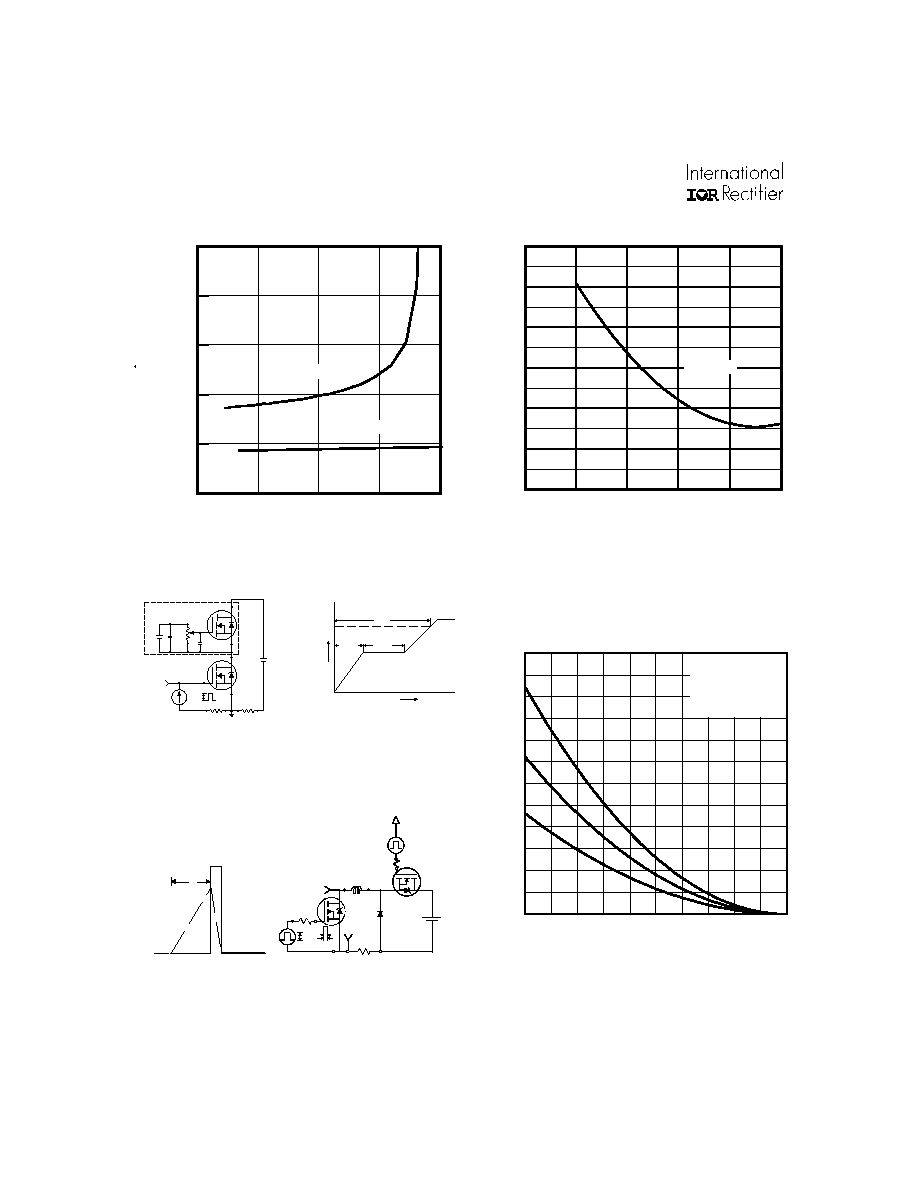
Fig 13. On-Resistance Vs. Gate Voltage
Fig 12. On-Resistance Vs. Drain Current
Fig 14a&b. Basic Gate Charge Test Circuit
and Waveform
Fig 15a&b. Unclamped Inductive Test circuit
and Waveforms
Fig 15c. Maximum Avalanche Energy
Vs. Drain Current
D.U.T.
V
DS
I
D
I
G
3mA
V
GS
.3
µ
F
50K
.2
µ
F
12V
Current Regulator
Same Type as D.U.T.
Current Sampling Resistors
+
-
V
GS
Q
G
Q
GS
Q
GD
V
G
Charge
tp
V(BR)DSS
IAS
R G
IAS
0.01
tp
D.U.T
L
VDS
+
-
VDD
DRIVER
A
15V
20V
25
50
75
100
125
150
0
50
100
150
200
250
300
Starting T , Junction Temperature ( C)
E ,
Si
ngl
e Pul
s
e Aval
anche Ener
gy (
m
J)
J
AS
∞
ID
TOP
BOTTOM
3.2A
4.6A
7.2A
0
20
40
60
80
ID , Drain Current (A)
0.004
0.008
0.012
0.016
0.020
0.024
R
D
S
(
o
n
)
,
D
r
a
i
n
-
t
o
-
S
o
u
r
c
e
O
n
R
e
s
i
s
t
a
n
c
e
(
)
VGS = 10V
VGS = 4.5V
3.2
3.3
3.4
3.5
3.6
3.7
VGS, Gate -to -Source Voltage (V)
0.00
0.01
0.02
0.03
0.04
0.05
0.06
R
D
S
(
o
n
),
D
r
a
i
n
-
t
o
-
S
o
u
r
c
e
O
n
R
e
s
i
s
t
a
n
c
e
(
)
ID = 7.2A
IRF7413
www.irf.com
7
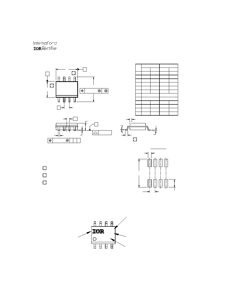
SO-8 Package Details
SO-8 Part Marking
EXAMPLE: T HIS IS AN IRF7101 (MOSFET )
INT ERNAT IONAL
RECT IFIER
LOGO
F7101
YWW
XXXX
PART NUMBER
LOT CODE
WW = WEEK
Y = LAST DIGIT OF T HE YEAR
DAT E CODE (YWW)
e 1
D
E
y
b
A
A1
H
K
L
.189
.1497
0∞
.013
.050 BAS IC
.0532
.0040
.2284
.0099
.016
.1968
.1574
8∞
.020
.0688
.0098
.2440
.0196
.050
4.80
3.80
0.33
1.35
0.10
5.80
0.25
0.40
0∞
1.27 BASIC
5.00
4.00
0.51
1.75
0.25
6.20
0.50
1.27
MIN
MAX
MILLIMET ERS
INCHES
MIN
MAX
DIM
8∞
e
c
.0075
.0098
0.19
0.25
.025 BAS IC
0.635 BASIC
8
7
5
6
5
D
B
E
A
e
6X
H
0.25 [.010]
A
6
7
K x 45∞
8X L
8X c
y
0.25 [.010]
C A B
e1
A
A1
8X b
C
0.10 [.004]
4
3
1
2
FOOT PRINT
8X 0.72 [.028]
6.46 [.255]
3X 1.27 [.050]
4. OUT LINE CONF ORMS T O JEDEC OUT LINE MS -012AA.
NOTES:
1. DIMENSIONING & T OLERANCING PER ASME Y14.5M-1994.
2. CONT ROLLING DIMENSION: MILLIMETER
3. DIMENSIONS ARE S HOWN IN MILLIMET ERS [INCHES].
5 DIMENSION DOES NOT INCLUDE MOLD PROTRUSIONS .
6 DIMENSION DOES NOT INCLUDE MOLD PROTRUSIONS .
MOLD PROTRUSIONS NOT T O EXCEED 0.25 [.010].
7 DIMENSION IS THE LENGTH OF LEAD F OR SOLDERING TO
A S UBS TRATE.
MOLD PROTRUSIONS NOT T O EXCEED 0.15 [.006].
8X 1.78 [.070]

IRF7413
8
www.irf.com
Repetitive rating; pulse width limited by
max. junction temperature.
Notes:
Starting T
J
= 25∞C, L = 4.4mH
R
G
= 25
, I
AS
= 7.2A.
Pulse width
300µs; duty cycle
2%.
When mounted on 1 inch square copper board
330.00
(12.992)
MAX.
14.40 ( .566 )
12.40 ( .488 )
NOTES :
1. CONTROLLING DIMENSION : MILLIMETER.
2. OUTLINE CONFORMS TO EIA-481 & EIA-541.
FEED DIRECTION
TERMINAL NUMBER 1
12.3 ( .484 )
11.7 ( .461 )
8.1 ( .318 )
7.9 ( .312 )
NOTES:
1. CONTROLLING DIMENSION : MILLIMETER.
2. ALL DIMENSIONS ARE SHOWN IN MILLIMETERS(INCHES).
3. OUTLINE CONFORMS TO EIA-481 & EIA-541.
SO-8 Tape and Reel
IR WORLD HEADQUARTERS: 233 Kansas St., El Segundo, California 90245, USA Tel: (310) 252-7105
TAC Fax: (310) 252-7903
Visit us at www.irf.com for sales contact information.3/02
Data and specifications subject to change without notice.
This product has been designed and qualified for the Automotive [Q101]
market.
Qualification Standards can be found on IR's Web site.
C
oss
eff. is a fixed capacitance that gives the same charging time
as C
oss
while V
DS
is rising from 0 to 80% V
DSS
I
SD
7.2A, di/dt
120A/µs, V
DD
V
(BR)DSS
,
T
J
150∞C