 | –≠–ª–µ–∫—Ç—Ä–æ–Ω–Ω—ã–π –∫–æ–º–ø–æ–Ω–µ–Ω—Ç: 80RIA80 | –°–∫–∞—á–∞—Ç—å:  PDF PDF  ZIP ZIP |
I
T(AV)
80
A
@ T
C
85
∞C
I
T(RMS)
125
A
I
TSM
@
50Hz
1900
A
@ 60Hz
1990
A
I
2
t
@
50Hz
18
KA
2
s
@ 60Hz
16
KA
2
s
V
DRM
/V
RRM
400 to 1200
V
t
q
typical
110
µs
T
J
- 40 to 125
∞C
Parameters
80RIA
Unit
Typical Applications
DC motor controls
Controlled DC power supplies
AC controllers
Features
Hermetic glass-metal seal
International standard case TO-209AC (TO-94)
Major Ratings and Characteristics
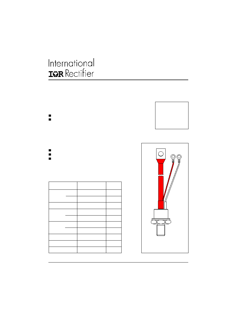
case style
TO-209AC (TO-94)
PHASE CONTROL THYRISTORS
Stud Version
80RIA SERIES
1
80A
Bulletin I25201 rev. B 03/03
www.irf.com
80RIA Series
2
Bulletin I25201 rev. B 03/03
www.irf.com
I
T(AV)
Max. average on-state current
80
A
180∞ conduction, half sine wave
@ Case temperature
85
∞C
I
T(RMS)
Max. RMS on-state current
125
A
DC @ 75∞C case temperature
I
TSM
Max. peak, one-cycle
1900
t = 10ms
No voltage
non-repetitive surge current
1990
t = 8.3ms
reapplied
1600
t = 10ms
100% V
RRM
1675
t = 8.3ms
reapplied
Sinusoidal half wave,
I
2
t
Maximum I
2
t for fusing
18
t = 10ms
No voltage
Initial T
J
= T
J
max.
16
t = 8.3ms
reapplied
12.7
t = 10ms
100% V
RRM
11.7
t = 8.3ms
reapplied
I
2
t
Maximum I
2
t for fusing
180.5
KA
2
s
t = 0.1 to 10ms, no voltage reapplied
V
T(TO)1
Low level value of threshold
voltage
V
T(TO)
2
High level value of threshold
voltage
r
t1
Low level value of on-state
slope resistance
r
t2
High level value of on-state
slope resistance
V
TM
Max. on-state voltage
1.60
V
I
pk
= 250A, T
J
= 25∞C t
p
= 10ms sine pulse
I
H
Maximum holding current
200
I
L
Typical latching current
400
0.99
(16.7% x
x I
T(AV)
< I <
x I
T(AV)
), T
J
= T
J
max.
2.29
(16.7% x
x I
T(AV)
< I <
x I
T(AV)
), T
J
= T
J
max.
1.84
(I >
x I
T(AV)
),T
J
= T
J
max.
Parameter
80RIA
Units
Conditions
1.13
(I >
x I
T(AV)
),T
J
= T
J
max.
On-state Conduction
KA
2
s
m
V
A
mA
T
J
= 25∞C, anode supply 12V resistive load
ELECTRICAL SPECIFICATIONS
Voltage Ratings
Voltage
V
DRM
/V
RRM
, max. repetitive
V
RSM
, maximum non-
I
DRM
/I
RRM
max.
Type number
Code
peak and off-state voltage
repetitive peak voltage
@ T
J
= 125∞C
V
V
mA
40
400
500
80RIA
80
800
900
15
120
1200
1300
80RIA Series
3
Bulletin I25201 rev. B 03/03
www.irf.com
di/dt
Max. non-repetitive rate of rise
T
J
= 125∞C, V
d
= rated V
DRM
, I
TM
= 2xdi/dt snubber
of turned-on current
300
A/µs 0.2µF, 15
, Gate pulse: 20V, 65
, t
p
= 6µs, t
r
= 0.5µs
Per JEDEC Standard RS-397, 5.2.2.6.
Gate pulse: 10V, 15
source, t
p
= 6µs, t
r
= 0.1µs,
V
d
= rated V
DRM
,
I
TM
= 50Adc,
T
J
= 25∞C.
I
TM
= 50A, T
J
= T
J
max, di/dt
= -5A/µs min., V
R
= 50V,
dv/dt
= 20V/µs, Gate bias: 0V 25
, t
p
= 500µs
dv/dt Maximum critical rate of rise of
off-state voltage
I
RRM
Max. peak reverse and off-state
I
DRM
leakage current
Blocking
Parameter
80RIA
Units
Conditions
15
mA
T
J
= 125∞C rated V
DRM
/V
RRM
applied
P
GM
Maximum peak gate power
12
T
J
= T
J
max, t
p
5ms
P
G(AV)
Maximum average gate power
3
T
J
= T
J
max, f = 50Hz, d% = 50
I
GM
Max. peak positive gate current
3
A
T
J
= T
J
max, t
p
5ms
+V
GM
Maximum peak positive
gate voltage
-V
GM
Maximum peak negative
gate voltage
I
GT
Max. DC gate current required
270
T
J
= - 40∞C
to trigger
120
mA
T
J
= 25∞C
60
T
J
= 125∞C
V
GT
Max. DC gate voltage required
3.5
T
J
= - 40∞C
to trigger
2.5
V
T
J
= 25∞C
1.5
T
J
= 125∞C
I
GD
DC gate current not to trigger
6
mA
Parameter
80RIA
Units
Conditions
Triggering
W
20
10
V
T
J
= T
J
max, t
p
5ms
V
GD
DC gate voltage not to trigger
0.25
V
Max. gate current/ voltage not to
trigger is the max. value which
will not trigger any unit with rated
V
DRM
anode-to-cathode applied
T
J
= T
J
max
Max. required gate trigger/ cur-
rent/ voltage are the lowest value
which will trigger all units 6V an-
ode-to-cathode applied
Parameter
80RIA
Units
Conditions
Switching
µs
500
V/µs
T
J
= 125∞C exponential to 67% rated V
DRM
t
d
Typical delay time
1
t
q
Typical turn-off time
110
80RIA Series
4
Bulletin I25201 rev. B 03/03
www.irf.com
180∞
0.042
0.030
120∞
0.050
0.052
90∞
0.064
0.070
K/W
T
J
= T
J
max.
60∞
0.095
0.100
30∞
0.164
0.165
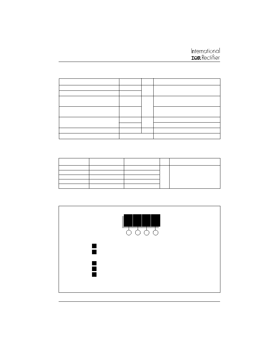
Ordering Information Table
1
-
I
TAV
x 10A
2
-
0 = Eyelet terminals (Gate and Auxiliary Cathode Leads)
1 = Fast - on terminals (Gate and Auxiliary Cathode Leads)
3
-
RIA = Essential part number
4
-
Voltage code: Code x 10 = V
RRM
(See Voltage Rating Table)
5
-
None = Stud base 1/2"-20UNF- 2A threads
NOTE: For Metric Device M12 x 1.75 E6 Contact factory
4
8
0
RIA 120
Device Code
1
2
T
J
Max. operating temperature range
-40 to 125
T
stg
Max. storage temperature range
-40 to 150
R
thJC
Max. thermal resistance,
junction to case
R
thCS
Max. thermal resistance,
case to heatsink
T
Mounting torque, ± 10%
15.5 (137)
Non lubricated threads
14 (120)
Lubricated threads
wt
Approximate weight
130
g
Parameter
80RIA
Units
Conditions
0.30
DC operation
0.1
Mounting surface, smooth, flat and greased
Thermal and Mechanical Specification
∞C
K/W
Nm
(lbf-in)
3
Case style
TO-209AC(TO-94)
See Outline Table
Conduction angle Sinusoidal conduction Rectangular conduction Units
Conditions
R
thJ-C
Conduction
(The following table shows the increment of thermal resistence R
thJ-C
when devices operate at different conduction angles than DC)
80RIA Series
5
Bulletin I25201 rev. B 03/03
www.irf.com
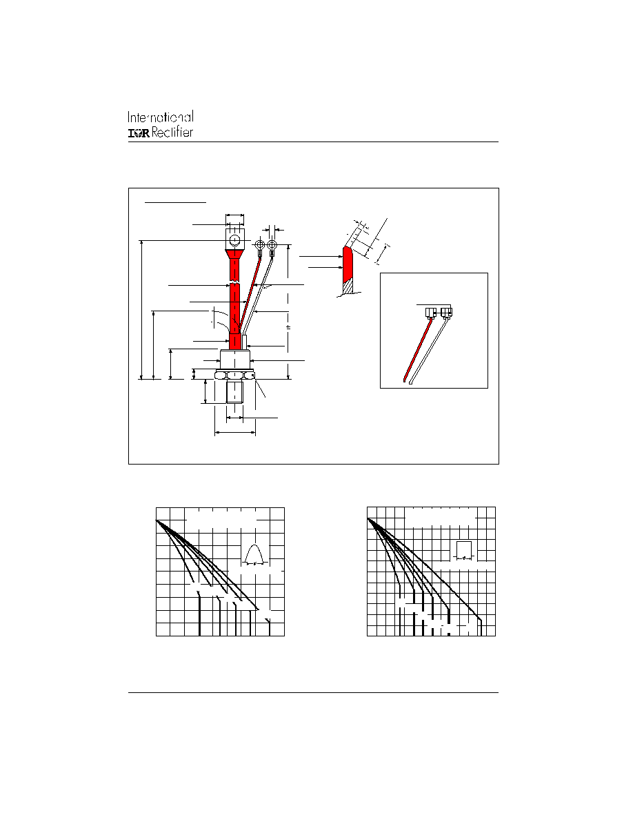
Outline Table
Fast-on Terminals
Case Style TO-209AC (TO-94)
All dimensions in millimeters (inches)
WHITE SHRINK
C.S. 0.4 mm 2
215 (8.46)
10 (0.39)
WHITE GATE
RED SHRINK
RED CATHODE
RED SILICON RUBBER
4.3 (0.17) DIA.
21 (
0
.
8
3
)
10
(
0
.
39)
M
A
X
.
1
57 (
6
.
18)
17
0 (
6
.
6
9)
(.0006 s.i.)
GLASS METAL SEAL
8.5 (0.3) DIA.
16.5 (0.65) MAX.
23.5 (0.92) MAX. DIA.
MA
X
.
24 (
0
.
9
4
)
M
A
X
.
55
(
2
.
17)
M
I
N
.
C.S. 16mm 2
FLEXIBLE LEAD
(.025 s.i.)
2.5 (0.10) MAX.
20
(0
.7
9)
M
IN
.
1/2"-20UNF-2A *
SW 27
29.5 (1.16) MAX.
9.
5
(0
.3
7)
M
IN
.
AMP. 280000-1
REF-250
* FOR METRIC DEVICE: M12 X 1.75 E6
CONTACT FACTORY
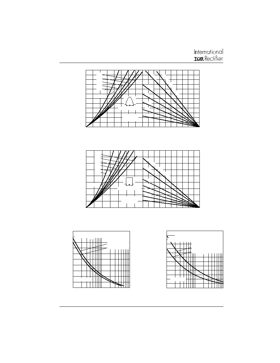
Fig. 1 - Current Ratings Characteristics
Fig. 2 - Current Ratings Characteristics
80
90
100
110
120
130
0
10 20 30 40 50 60 70 80 90
M
a
x
i
mu
m
A
l
l
o
wabl
e
C
a
s
e
T
e
mp
e
r
atu
r
e
(
∞
C
)
30∞
60∞
90∞
120∞
180∞
Average On-state Current (A)
Conduc tion Angle
80RIA Series
R (DC) = 0.30 K/ W
thJC
70
80
90
100
110
120
130
0
20
40
60
80
100 120 140
DC
30∞
60∞
90∞
120∞
180∞
Average On-state Current (A)
Ma
x
i
m
u
m A
l
l
o
w
a
b
l
e Ca
s
e
T
e
m
p
e
r
a
t
u
r
e
(
∞
C
)
Conduction Period
80RIA Series
R (DC) = 0.30 K/ W
thJC
80RIA Series
6
Bulletin I25201 rev. B 03/03
www.irf.com
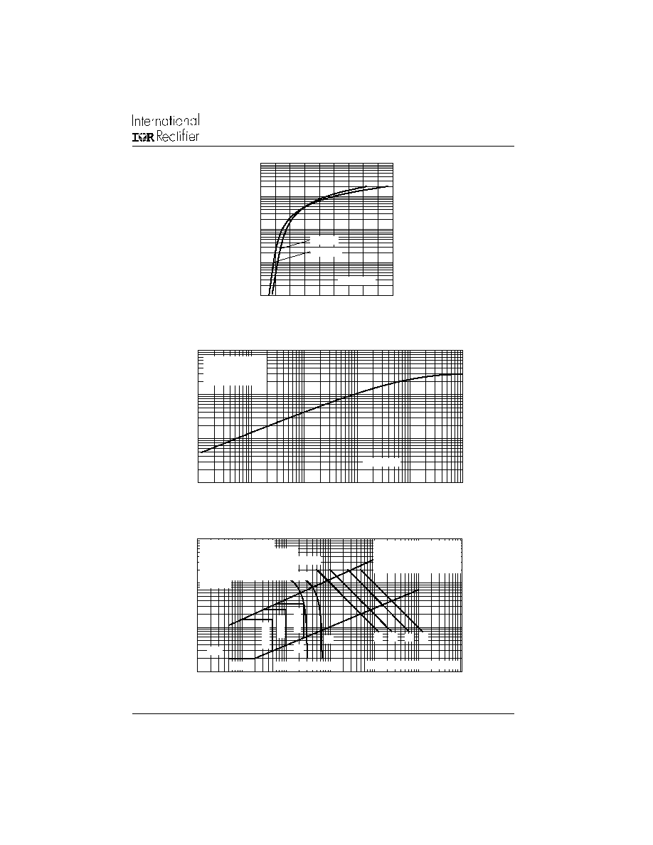
0
25
50
75
100
125
Maximum Allowable Ambient Temperature (∞C)
0.6
K/
W
1 K
/W
2 K/W
5 K/W
3 K/ W
1.4 K
/ W
R
= 0
.4
K
/W
- D
elt
a
R
th
SA
0
10
20
30
40
50
60
70
80
90
100
110
120
0
10
20
30
40
50
60
70
80
180∞
120∞
90∞
60∞
30∞
RMS Limit
Conduction Angle
M
a
x
i
m
u
m
A
v
e
r
a
g
e
O
n
-s
t
a
t
e
P
o
w
e
r L
o
s
s
(
W
)
Average On-state Current (A)
80RIA Series
T = 125∞C
J
Fig. 3 - On-state Power Loss Characteristics
0
25
50
75
100
125
Maximum Allowable Ambient Temperature (∞C)
R
= 0
.4 K
/ W
- D
elta
R
thS
A
0.6
K/W
1 K/
W
1.4 K
/W
2 K/ W
3 K/ W
5 K/ W
0
20
40
60
80
100
120
140
160
180
0
20
40
60
80
100 120 140
DC
180∞
120∞
90∞
60∞
30∞
RMS Limit
Conduc tion Period
M
a
x
i
mu
m A
v
e
r
a
g
e
O
n
-
s
t
a
t
e
P
o
we
r
L
o
s
s
(
W
)
Average On-state Current (A)
80RIA Series
T = 125∞C
J
Fig. 4 - On-state Power Loss Characteristics
800
1000
1200
1400
1600
1800
1
10
100
Number Of Equa l Amplitude Half Cycle Current Pulses (N)
P
e
a
k
H
a
l
f
S
i
n
e
W
a
v
e
On
-
s
t
a
t
e
C
u
r
r
e
n
t
(
A
)
Initial T = 125∞C
@ 60 Hz 0.0083 s
@ 50 Hz 0.0100 s
J
80RIA Series
At Any Rated Load Condition And With
Rated V Applied Following Surge.
RRM
700
800
900
1000
1100
1200
1300
1400
1500
1600
1700
1800
1900
2000
0.01
0.1
1
Pulse Train Duration (s)
Versus Pulse Train Duration. Control
Of Conduction May Not Be Maintained.
P
e
a
k
H
a
l
f
S
i
n
e
W
a
v
e
O
n
-
s
ta
te C
u
r
r
e
n
t (
A
)
Initial T = 125∞C
No Voltage Reapplied
Rated V Reapplied
RRM
J
80RIA Series
Maximum Non Repetitive Surge Current
Fig. 5 - Maximum Non-Repetitive Surge Current
Fig. 6 - Maximum Non-Repetitive Surge Current
80RIA Series
7
Bulletin I25201 rev. B 03/03
www.irf.com
Fig. 7 - On-state Voltage Drop Characteristics
1
10
100
1000
10000
0.5 1
1.5 2
2.5 3
3.5
4
4.5 5
T = 25∞C
J
I
n
s
t
an
t
a
ne
ou
s
O
n
-
s
t
a
t
e
C
u
r
r
e
n
t
(
A
)
Instantaneous On-state Voltage (V)
T = 125∞C
J
80RIA Series
Fig. 8 - Thermal Impedance Z
thJC
Characteristics
0.001
0.01
0.1
1
0.0001
0.001
0.01
0.1
1
10
Square Wave Pulse Duration (s)
th
J
C
80RIA Series
Steady State Value
R = 0.30 K/ W
(DC Operation)
T
r
an
s
i
e
n
t
T
h
e
r
m
a
l
I
m
pe
da
n
c
e
Z
(
K
/
W
)
thJC
Fig. 9 - Gate Characteristics
0.1
1
10
100
0.001
0.01
0.1
1
10
100
1000
VGD
IGD
(b)
(a)
Tj
=
2
5
∞
C
Tj
=
1
2
5
∞
C
Tj
=
-
4
0
∞
C
(1) (2)
(3)
Instantaneous Gate Current (A)
I
n
s
t
an
t
ane
ou
s
G
a
t
e
V
o
l
t
ag
e
(
V
)
Rectangular gate pulse
a) Recommended load line for
b) Recommended load line for
Frequency Limited by PG(AV)
tr<=1 µs
rated di/ dt : 20V, 30ohms; tr<=0.5 µs
<=30% rated di/ dt : 20V, 65ohms
(1) PGM = 100W, tp = 500µs
(2) PGM = 50W, tp = 1ms
(3) PGM = 20W, tp = 2.5ms
(4) PGM = 10W, tp = 5ms
Device: 80RIA Series
(4)
80RIA Series
8
Bulletin I25201 rev. B 03/03
www.irf.com
IR WORLD HEADQUARTERS: 233 Kansas St., El Segundo, California 90245, USA Tel: (310) 252-7105
TAC Fax: (310) 252-7309
Visit us at www.irf.com for sales contact information. 03 /03
Data and specifications subject to change without notice.
This product has been designed and qualified for Industrial Level.
Qualification Standards can be found on IR's Web site.

This datasheet has been download from:
www.datasheetcatalog.com
Datasheets for electronics components.