
PHASE CONTROL SCR
1
Preliminary Data Sheet I2132 rev. C 10/99
V
T
< 1.2 V @ 8A
I
TSM
= 120A
V
R
/ V
D
= up to 800V
SAFE
IR
Series
8TWS..S
Major Ratings and Characteristics
I
T(AV)
Sinusoidal waveform
8
A
I
RMS
12
A
V
RRM
/ V
DRM
up to 800
V
I
TSM
120
A
V
T
@ 8 A, T
J
= 25�C
1.2
V
dv/dt
200
V/�s
di/dt
150
A/�s
T
J
- 40 to 125
�C
Characteristics
8TWS..S
Units
TO-252AA (D-Pak )
Description/Features
The 8TWS..S
SAFE
IR
new series of silicon
controlled rectifiers in D-Pak, are specifically
designed for low power switching and phase
control applications. The glass passivation
technology used has reliable operation up to
125�C junction temperature.
Typical applications are in input rectification
(soft start), AC switches, Motor Control and
Crow-Bar. These products are designed to be
used with International Rectifier input diodes,
switches and output rectifiers which are avail-
able in identical package outlines.
Package Outline

2
8TWS..S
SAFE
IR
Series
Preliminary Data Sheet I2132 rev. C 10/99
Voltage Ratings
Part Number
V
RRM
/ V
DRM
, max. repetitive
V
RSM
, maximum non repetitive
I
RRM
/ I
DRM
peak and off-state voltage
peak reverse voltage
125�C
V
V
mA
8TWS04S
400
500
5
8TWS06S
600
700
8TWS08S
800
900
I
T(AV)
Max. Average On-state Current
8
A
@ T
C
= 95� C, 180� conduction half sine wave
I
RMS
Max. RMS On-state Current
1 2
I
TSM
Max. Peak One Cycle
100
10ms Sine pulse, rated V
RRM
applied,
T
J
= 125�C
Non-Repetitive Surge Current
120
10ms Sine pulse, no voltage reapplied, T
J
= 125�C
I
2
t
Max. I
2
t for fusing
45
A
2
s
10ms Sine pulse, rated V
RRM
applied,T
J
= 125�C
70
10ms Sine pulse, no voltage reapplied` T
J
= 125�C
I
2
t
Max. I
2
t for fusing
700
A
2
s
t = 0.1 to 10ms, no voltage reapplied
V
TM
Max. On-state Voltage Drop
1.2
V
@ 8A, T
J
= 25�C
r
t
On-state slope resistance
2724
m
T
J
= 125�C
V
T(TO)
Threshold Voltage
1.011
V
I
RM
/ I
DM
Max.Reverse and Direct
0.05
mA
T
J
= 25 �C
Leakage Current
5
T
J
= 125 �C
I
H
Max. Holding Current
85
mA
Anode Supply = 6V, Resistive load, Initial I
T
=1A
I
L
Max. Latching Current
75
mA
Anode Supply = 6V, Resistive load
dv/dt
Max. rate of rise of off-state Voltage
200
V/�s
di/dt
Max. rate of rise of turned-on Current
150
A/�s
Absolute Maximum Ratings
Parameters
8TWS..S
Units
Conditions
V
R
= rated V
RRM
/ V
DRM
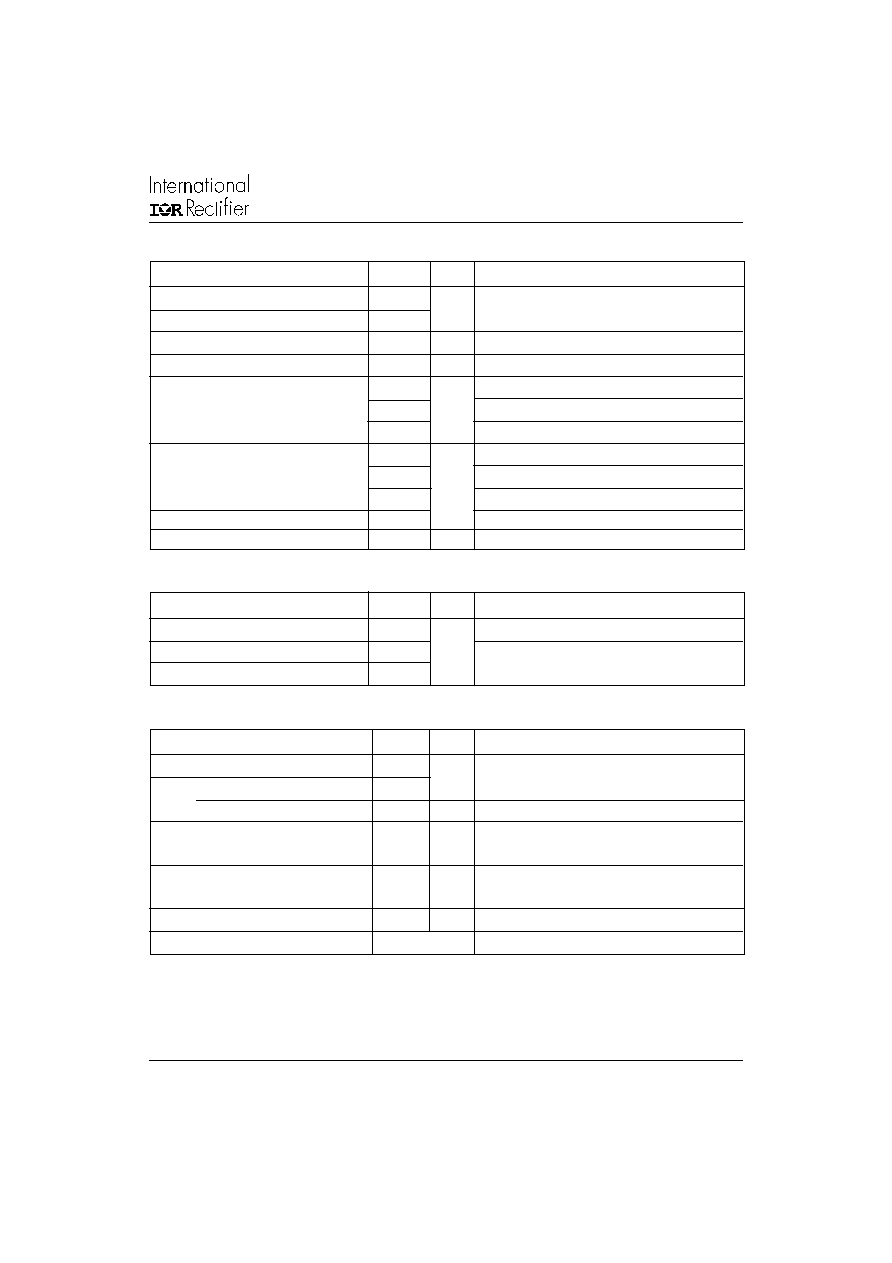
3
8TWS..S
SAFE
IR
Series
Preliminary Data Sheet I2132 rev. C 10/99
Thermal-Mechanical Specifications
T
J
Max. Junction Temperature Range - 40 to 125
�C
T
stg
Max. Storage Temperature Range
- 40 to 125
Soldering Temperature
240
�C
for 10 seconds (1.6mm from case)
R
thJC
Max. Thermal Resistance Junction
2.0
�C/W
DC operation
to Case
R
thJA
Max. Thermal Resistance Junction
65
�C/W
to Ambient (PCB Mount)**
wt
Approximate Weight
1(0.03)
g (oz.)
T
Case Style
TO-252AA (D-PAK)
Parameters
8TWS..S Units
Conditions
Triggering
P
GM
Max. peak Gate Power
8.0
W
P
G(AV)
Max. average Gate Power
2.0
+ I
GM
Max. paek positive Gate Current
1.5
A
- V
GM
Max. paek negative Gate Voltage
10
V
I
GT
Max. required DC Gate Current
20
mA
Anode supply = 6V, resistive load, T
J
= - 10�C
to trigger
15
Anode supply = 6V, resistive load, T
J
= 25�C
10
Anode supply = 6V, resistive load, T
J
= 125�C
V
GT
Max. required DC Gate Voltage
1.2
V
Anode supply = 6V, resistive load, T
J
= - 10�C
to trigger
1
Anode supply = 6V, resistive load, T
J
= 25�C
0.75
Anode supply = 6V, resistive load, T
J
= 125�C
V
GD
Max. DC Gate Voltage not to trigger
0.20
T
J
= 125�C, V
DRM
= rated value
I
GD
Max. DC Gate Current not to trigger
0.10
mA
T
J
= 125�C, V
DRM
= rated value
Parameters
8TWS..S
Units
Conditions
Switching
Parameters
8TWS..S
Units
Conditions
t
gt
Typical turn-on time
0.8
�s
T
J
= 25�C
t
rr
Typical reverse recovery time
3
T
J
= 125�C
t
q
Typical turn-off time
100
**When mounted on 1" square (650mm
2
) PCB of FR-4 or G-10 material 4 oz (140�m) copper 40�C/W
For recommended footprint and soldering techniques refer to application note #AN-994

4
8TWS..S
SAFE
IR
Series
Preliminary Data Sheet I2132 rev. C 10/99
Outline Table
Dimensions in millimeters and (inches)
Ordering Information Table
8
T
W
S
08
S
TRL
Device Code
1
5
2
4
3
1
-
Current Rating
2
-
Circuit Configuration:
T = Thyristor
3
-
Package:
W = TO-252AA (D-Pak)
4
-
Type of Silicon:
S = Standard Thyristors
5
-
Voltage code: Code x 100 = V
RRM
6
-
SMD Package
7
-
Tape and Reel Option
TRL = Left Reel
TRR = Right Orientation Reel
04 = 400V
06 = 600V
08 = 800V
6
7
(A)
(K)
(G)
4
1
3
6.73 (0.26)
6.35 (0.25)
5.46 (0.21)
5.21 (0.20)
4
1.27 (0.05)
0.88 ( 0.03)
5.97 (0.23)
1 - Anode
2 - Cathode
3 - G ate
4 - Anode
1.64 (0.02)
1.52 (0.06)
1.15 (0.04)
1.14 (0.04)
0.76 (0.03)
2x
2.28 (0.09)
2x
0.89 (0.03)
0.64 (0.02)
3x
4.57 (0.18)
1
2
3
6.22 (0.24)
2.38 (0.09)
2.19 (0.08)
6.45 (0.24)
5.68 (0.22)
10.42 (0.41)
9.40 (0.37)
0.46 (0.02)
0.58 (0.02)
1.14 (0.04)
0.89 (0.03)
0.51 (0.02)
MIN.
0.58 (0.02)
0.46 (0.02)
MINIMUM RECOMMENDED FOOTPRINT
5.97 (0.24)
10.67 (0.42)
1.65 (0.06)
6.48 (0.26)
2x
2.54 (0.10)
2x
2.28 ( 0.09)
2x

5
8TWS..S
SAFE
IR
Series
Preliminary Data Sheet I2132 rev. C 10/99
Marking Information
EXAMPLE: THIS IS AN 8TWS08S
9G3A
8TWS08S
9512
INTERNATIONAL
RECTIFIER LOGO
PART NUMBER
DATE CODE (YYWW)
YY = YEAR
WW = WEEK
ASSEMBLY
LOT CODE
Tape & Reel Information
TR
FEED DIRECTION
4.1 (0.16)
3.9 (0.15)
2.1 (0.83)
1.9 (0.07)
12.1 (0.48)
1.65 (0.06)
1.85 (0.07)
1.65 (0.06)
7.4 (0.29)
2.6 (0.10)
1.5 (0.06)
7.6 (0.30)
11.9 (0.47)
1.85 (0.07)
TO-252AA Tape & Reel
When ordering, indicate the part
number, part orientation, and the
quantity. Quantities are in multiples
of 2,000 pieces per reel for TR and
multiples of 3,000 pieces per reel
for both TRL and TRR.
13 (0.52) DIA.
DIA. MAX.
375 (14.17)
50 (1.97) DIA.
22.4 (0.88)
0.35 (0.01)
16.3 (0.64)
15.7 (0.62)
2.75 (0.11)
2.55 (0.10)
0.25 (0.01)
6.8 (0.26)
7.0 (0.28)
TRR
FEED DIRECTION
4.1 (0.16)
3.9 (0.15)
2.1 (0.83)
1.9 (0.07)
8.1 (0.32)
1.85 (0.07)
1.65 (0.06)
1.85 (0.07)
1.65 (0.06)
7.4 (0.29)
2.6 (0.10)
1.5 (0.06)
7.6 (0.30)
7.9 (0.31)
0.35 (0.01)
16.3 (0.64)
15.7 (0.62)
2.75 (0.11)
2.55 (0.10)
0.25 (0.01)
10.4 (0.41)
10.6 (0.42)
DIA.
TRL
FEED DIRECTION
4.1 (0.16)
3.9 (0.15)
2.1 (0.83)
1.9 (0.07)
8.1 (0.32)
1.85 (0.07)
1.65 (0.06)
1.85 (0.07)
1.65 (0.06)
7.4 (0.29)
2.6 (0.10)
1.5 (0.06)
7.6 (0.30)
7.9 (0.31)
0.35 (0.01)
16.3 (0.64)
15.7 (0.62)
2.75 (0.11)
2.55 (0.10)
0.25 (0.01)
10.4 (0.41)
10.6 (0.42)
DIA.
DIA.
DIA.
DIA.
DIA.
4 (A)
1 (K)
3 (G)