
07/09/02
www.irf.com
1
ADVANCED ANALOG
HIGH RELIABILITY
HYBRID DC/DC CONVERTERS
AFL50XXS SERIES
The AFL Series of DC/DC converters feature high power
density with no derating over the full military tempera-
ture range. This series is offered as part of a complete
family of converters providing single and dual output
voltages and operating from nominal +28, +50, +120 or
+270 volt inputs with output power ranging from 80 to
120 watts. For applications requiring higher output
power, individual converters can be operated in paral-
lel. The internal current sharing circuits assure equal
current distribution among the paralleled converters. This
series incorporates Advanced Analog's proprietary mag-
netic pulse feedback technology providing optimum
dynamic line and load regulation response. This feed-
back system samples the output voltage at the pulse
width modulator fixed clock frequency, nominally 550
KHz. Multiple converters can be synchronized to a sys-
tem clock in the 500 KHz to 700 KHz range or to the
synchronization output of one converter. Undervoltage
lockout, primary and secondary referenced inhibit, soft-
start and load fault protection are provided on all mod-
els.
These converters are hermetically packaged in two en-
closure variations, utilizing copper core pins to mini-
mize resistive DC losses. Three lead styles are avail-
able, each fabricated with Advanced Analog's rugged
ceramic lead-to-package seal assuring long term
hermeticity in the most harsh environments.
Description
n
30 To 80 Volt Input Range
n
3.3
,
5, 8, 9 12, 15, 24
and
28
Volts Outputs
Available
n
High Power Density - up to 84 W / in3
n
Up To 120 Watt Output Power
n
Parallel Operation with Stress and Current
Sharing
n
Low Profile (0.380") Seam Welded Package
n
Ceramic Feedthru Copper Core Pins
n
High Efficiency - to 85%
n
Full Military Temperature Range
n
Continuous Short Circuit and Overload
Protection
n
Remote Sensing Terminals
n
Primary and Secondary Referenced
Inhibit Functions
n
Line Rejection > 40 dB - DC to 50KHz
n
External Synchronization Port
n
Fault Tolerant Design
n
Dual Output Versions Available
n
Standard Military Drawings Available
Features
AFL
50V Input, Single Output
Manufactured in a facility fully qualified to MIL-PRF-
38534, these converters are available in four screening
grades to satisfy a wide range of requirements. The CH
grade is fully compliant to the requirements of MIL-H-
38534 for class H. The HB grade is fully processed and
screened to the class H requirement, may not neces-
sarily meet all of the other MIL-PRF-38534 requirements,
e.g., element evaluation and Periodic Inspection (P.I.)
not required. Both grades are tested to meet the com-
plete group "A" test specification over the full military
temperature range without output power deration.
Two grades with more limited screening are also
available for use in less demanding applications.
Variations in electrical, mechanical and screen-
ing can be accommodated. Contact Advanced
Analog for special requirements.
PD - 94457A

2
www.irf.com
AFL50XXS Series
Specifications
Static Characteristics -55�C < T
CASE
< +125�C, 30V< V
IN
< 80V
unless otherwise specified.
For Notes to Specifications, refer to page 4
ABSOLUTE MAXIMUM RATINGS
Input Voltage
-0.5V to 100V
Soldering Temperature
300�C for 10 seconds
Case Temperature
Operating
-55�C to +125�C
Storage
-65�C
to
+135�C
Parameter
Group A
Subgroups
Test Conditions
Min
Nom
Max
Unit
INPUT VOLTAGE
Note 6
30
50
80
V
OUTPUT VOLTAGE
AFL5005S
AFL5008S
AFL5009S
AFL5012S
AFL5015S
AFL5028S
AFL5005S
AFL5008S
AFL5009S
AFL5012S
AFL5015S
AFL5028S
1
1
1
1
1
1
2, 3
2, 3
2, 3
2, 3
2, 3
2, 3
VIN = 50 Volts, 100% Load
4.95
7.92
8.91
11.88
14.85
27.72
4.90
7.84
8.82
11.76
14.70
27.44
5.00
8.00
9.00
12.00
15.00
28.00
5.05
8.08
9.09
12.12
15.15
28.28
5.10
8.16
9.18
12.24
15.30
28.56
V
V
V
V
V
V
V
V
V
V
V
V
OUTPUT CURRENT
AFL5005S
AFL5008S
AFL5009S
AFL5012S
AFL5015S
AFL5028S
VIN = 30, 50, 80 Volts - Note 6
16.0
10.0
10.0
9.0
8.0
4.0
A
A
A
A
A
A
OUTPUT POWER
AFL5005S
AFL5008S
AFL5009S
AFL5012S
AFL5015S
AFL5028S
Note 6
80
80
90
108
120
112
W
W
W
W
W
W
MAXIMUM CAPACITIVE LOAD
Note
1
10,000
�
fd
OUTPUT VOLTAGE
TEMPERATURE COEFFICIENT
VIN = 50 Volts, 100% Load - Note 1, 6
-0.015 +0.015
%/�C
OUTPUT VOLTAGE REGULATION
AFL5028S
Line
All Others
Line
Load
1, 2, 3
1, 2, 3
1, 2, 3
No Load, 50% Load, 100% Load
VIN = 30, 50, 80 Volts
-70.0
-20.0
-1.0
+70.0
+20.0
+1.0
mV
mV
%
OUTPUT RIPPLE VOLTAGE
AFL5005S
AFL5008S
AFL5009S
AFL5012S
AFL5015S
AFL5028S
1, 2, 3
1, 2, 3
1, 2, 3
1, 2, 3
1, 2, 3
1, 2, 3
VIN = 30, 50, 80 Volts, 100% Load,
BW = 10MHz
30
40
40
45
50
100
mVpp
mVpp
mVpp
mVpp
mVpp
mVpp

www.irf.com
3
AFL50XXS Series
Static Characteristics
(Continued)
For Notes to Specifications, refer to page 4
Parameter
Group A
Subgroups
Test Conditions
Min
Nom
Max
Unit
INPUT CURRENT
No
Load
Inhibit
1
Inhibit
2
1
2, 3
1, 2, 3
1, 2, 3
VIN = 50 Volts
IOUT = 0
Pin 4 Shorted to Pin 2
Pin 12 Shorted to Pin 8
50
60
5
5
mA
mA
mA
mA
INPUT RIPPLE CURRENT
AFL5005S
AFL5008S
AFL5009S
AFL5012S
AFL5015S
AFL5028S
1, 2, 3
1, 2, 3
1, 2, 3
1, 2, 3
1, 2, 3
1, 2, 3
VIN = 50 Volts, 100% Load, BW = 10MHz
60
60
60
60
60
60
mApp
mApp
mApp
mApp
mApp
mApp
CURRENT LIMIT POINT
As a percentage of full rated load
1
2
3
VOUT = 90% VNOM , VIN = 50 Volts
Note 5
115
105
125
125
115
140
%
%
%
LOAD FAULT POWER DISSIPATION
Overload or Short Circuit
1, 2, 3
V
IN
= 50 Volts
32
W
EFFICIENCY
AFL5005S
AFL5008S
AFL5009S
AFL5012S
AFL5015S
AFL5028S
1, 2, 3
1, 2, 3
1, 2, 3
1, 2, 3
1, 2, 3
1, 2, 3
V
IN
= 50 Volts, 100% Load
78
79
80
81
82
82
81
82
83
84
85
84
%
%
%
%
%
%
ENABLE INPUTS (Inhibit Function)
Converter Off
Sink
Current
Converter
On
Sink
Current
1, 2, 3
1, 2, 3
Logical Low on Pin 4 or Pin 12
Note 1
Logical High on Pin 4 and Pin 12 - Note 9
Note 1
-0.5
2.0
0.8
100
50
100
V
�
A
V
�
A
SWITCHING FREQUENCY
1, 2, 3
500
550
600
KHz
SYNCHRONIZATION INPUT
Frequency Range
Pulse
Amplitude,
Hi
Pulse
Amplitude,
Lo
Pulse Rise Time
Pulse Duty Cycle
1, 2, 3
1, 2, 3
1, 2, 3
Note 1
Note 1
500
2.0
-0.5
20
700
10
0.8
100
80
KHz
V
V
nSec
%
ISOLATION
1
Input to Output or Any Pin to Case
(except Pin 3). Test @ 500VDC
100
M
DEVICE WEIGHT
Slight Variations with Case Style
85
gms
MTBF
MIL-HDBK-217F, AIF @ TC = 40�C
300
KHrs

4
www.irf.com
AFL50XXS Series
Dynamic Characteristics -55�C < T
CASE
< +125�C, V
IN
=50V
unless otherwise specified.
Parameter
Group A
Subgroups
Test Conditions
Min
Nom
Max
Unit
LOAD TRANSIENT RESPONSE
AFL5005S Amplitude
Recovery
Amplitude
Recovery
AFL5008S Amplitude
Recovery
Amplitude
Recovery
AFL5009S Amplitude
Recovery
Amplitude
Recovery
AFL5012S
Amplitude
Recovery
Amplitude
Recovery
AFL5015S
Amplitude
Recovery
Amplitude
Recovery
AFL5028S Amplitude
Recovery
Amplitude
Recovery
4, 5, 6
4, 5, 6
4, 5, 6
4, 5, 6
4, 5, 6
4, 5, 6
4, 5, 6
4, 5, 6
4, 5, 6
4, 5, 6
4, 5, 6
4, 5, 6
4, 5, 6
4, 5, 6
4, 5, 6
4, 5, 6
4, 5, 6
4, 5, 6
4, 5, 6
4, 5, 6
4, 5, 6
4, 5, 6
4, 5, 6
4, 5, 6
Note 2, 8
Load Step 50%
100%
Load Step 10%
50%
Load Step 50%
100%
Load Step 10%
50%
Load Step 50%
100%
Load Step 10%
50%
Load Step 50%
100%
Load Step 10%
50%
Load Step 50%
100%
Load Step 10%
50%
Load Step 50%
100%
Load Step 10%
50%
-450
-450
-500
-500
-600
-600
-750
-750
-750
-750
-1200
-1200
450
200
450
300
500
200
500
300
600
200
600
300
750
200
750
300
750
200
750
300
1200
200
1200
300
mV
�
Sec
mV
�
Sec
mV
�
Sec
mV
�
Sec
mV
�
Sec
mV
�
Sec
mV
�
Sec
mV
�
Sec
mV
�
Sec
mV
�
Sec
mV
�
Sec
mV
�
Sec
LINE TRANSIENT RESPONSE
Amplitude
Recovery
Note 1, 2, 3
VIN Step = 30
80 Volts
-500
500
500
mV
�
Sec
TURN-ON CHARACTERISTICS
Overshoot
Delay
4, 5, 6
4, 5, 6
VIN = 30, 50, 80 Volts. Note 4
Enable 1, 2 on. (Pins 4, 12 high or
open)
50
75
250
120
mV
mSec
LOAD FAULT RECOVERY
Same as Turn On Characteristics.
LINE REJECTION
MIL-STD-461D, CS101, 30Hz to 50KHz
Note 1
40 50 dB
Notes to Specifications:
1.
Parameters not 100% tested but are guaranteed to the limits specified in the table.
2.
Recovery time is measured from the initiation of the transient to where VOUT has returned to within
�
1% of VOUT at 50% load.
3.
Line transient transition time
100
�
Sec.
4.
Turn-on delay is measured with an input voltage rise time of between 100 and 500 volts per millisecond.
5.
Current limit point is that condition of excess load causing output voltage to drop to 90% of nominal.
6.
Parameter verified as part of another test.
7.
All electrical tests are performed with the remote sense leads connected to the output leads at the load.
8.
Load transient transition time
10
�
Sec.
9.
Enable inputs internally pulled high. Nominal open circuit voltage
4.0VDC.
www.irf.com
5
AFL50XXS Series
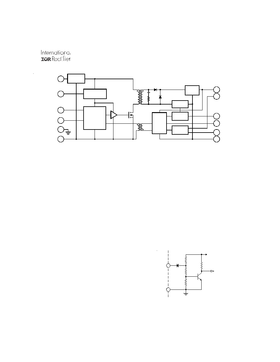
AFL50XXS Circuit Description
Figure I. AFL Single Output Block Diagram
Figure II. Enable Input Equivalent Circuit
Circuit Operation and Application Information
Inhibiting Converter Output
As an alternative to application and removal of the DC volt-
age to the input, the user can control the converter output
by providing TTL compatible, positive logic signals to either
of two enable pins (pin 4 or 12). The distinction between
these two signal ports is that enable 1 (pin 4) is referenced
to the input return (pin 2) while enable 2 (pin 12) is refer-
enced to the output return (pin 8). Thus, the user has
access to an inhibit function on either side of the isolation
barrier. Each port is internally pulled "high" so that when not
used, an open connection on both enable pins permits nor-
mal converter operation. When their use is desired, a logi-
cal "low" on either port will shut the converter down.
1
DC Input
Enable 1
4
Sync Output
5
6
Sync Input
Case
3
2
Input Return
Input
Filter
Primary
Bias Supply
Control
FB
Output
Filter
Current
Sense
Error
Amp
& Ref
Share
Amplifier
Sense
Amplifier
7
+Output
10
+Sense
11
Share
12
Enable 2
9
-Sense
8
Output Return
The AFL series of converters employ a forward switched
mode converter topology. (refer to Figure I.) Operation of
the device is initiated when a DC voltage whose magnitude
is within the specified input limits is applied between pins 1
and 2. If pin 4 is enabled (at a logical 1 or open) the primary
bias supply will begin generating a regulated housekeeping
voltage bringing the circuitry on the primary side of the
converter to life. A power MOSFET is used to chop the DC
input voltage into a high frequency square wave, applying
this chopped voltage to the power transformer at the nomi-
nal converter switching frequency. Maintaining a DC volt-
age within the specified operating range at the input as-
sures continuous generation of the primary bias voltage.
The switched voltage impressed on the secondary output
transformer winding is rectified and filtered to generate the
converter DC output voltage. An error amplifier on the sec-
ondary side compares the output voltage to a precision
reference and generates an error signal proportional to the
difference. This error signal is magnetically coupled through
the feedback transformer into the controller section of the
converter varying the pulse width of the square wave signal
driving the MOSFET, narrowing the width if the output volt-
age is too high and widening it if it is too low, thereby regulat-
ing the output voltage.
Remote Sensing
Connection of the + and - sense leads at a remotely located
load permits compensation for excessive resistance be-
tween the converter output and the load when their physical
separation could cause undesirable voltage drop. This con-
nection allows regulation to the placard voltage at the point
of application. When the remote sensing feature is not used,
the sense lead should be connected to their respective
output terminals at the converter. Figure III. illustrates a
typical remotely sensed application.
D isable
100K
290K
180K
1N 4 148
2N 3 904
+5.6 V
P in 4 o r
P in 12
P in 2 o r
P in 8