Äîêóìåíòàöèÿ è îïèñàíèÿ www.docs.chipfind.ru
09/01/04
www.irf.com
1
HIGH RELIABILITY
HYBRID DC/DC CONVERTER
AFL27003R3S
The AFL Series of DC/DC converters feature high power
density with no derating over the full military temperature
range. This series is offered as part of a complete family
of converters providing single and dual output voltages
and operating from nominal +28 or +270 volt inputs with
output power ranging from 80 to 120 watts. For
applications requiring higher output power, multiple
converters can be operated in parallel. The internal
current sharing circuits assure equal current distribution
among the paralleled converters. This series
incorporates International Rectifier's proprietary
magnetic pulse feedback technology providing optimum
dynamic line and load regulation response. This
feedback system samples the output voltage at the pulse
width modulator fixed clock frequency, nominally 550
KHz. Multiple converters can be synchronized to a system
clock in the 500 KHz to 700 KHz range or to the
synchronization output of one converter. Undervoltage
lockout, primary and secondary referenced inhibit, soft-
start and load fault protection are provided on all models.
These converters are hermetically packaged in two
enclosure variations, utilizing copper core pins to
minimize resistive DC losses. Three lead styles are
available, each fabricated with International Rectifier's
rugged ceramic lead-to-package seal assuring long
term hermeticity in the most harsh environments.
Manufactured in a facility fully qualified to MIL-PRF-
38534, these converters are available in four screening
grades to satisfy a wide range of requirements. The CH
grade is fully compliant to the requirements of MIL-PRF-
38534 for class H. The HB grade is fully processed and
screened to the class H requirement, but does not have
material element evaluated to the class H requirement.
Both grades are tested to meet the complete group "A"
test specification over the full military temperature range
without output power deration. Two grades with more
limited screening are also available for use in less
Description
demanding applications. Variations in electrical,
mechanical and screening can be accommodated.
Contact IR Santa Clara for special requirements.
n 160 To 400 Volt Input Range
n 3.3 Volt Output
n High Power Density - 46 W / in3
n 66 Watt Output Power
n Parallel Operation with Stress and Current
Sharing
n Low Profile (0.380") Seam Welded Package
n Ceramic Feedthru Copper Core Pins
n High Efficiency - to 74%
n Full Military Temperature Range
n Continuous Short Circuit and Overload
Protection
n Remote Sensing Terminals
n Primary and Secondary Referenced
Inhibit Functions
n Line Rejection > 60 dB - DC to 50KHz
n External Synchronization Port
n Fault Tolerant Design
n Dual Output Versions Available
n Standard Military Drawings Available
Features
AFL
270V Input, 3.3V Output
PD - 94462E
2
www.irf.com
AFL27003R3S
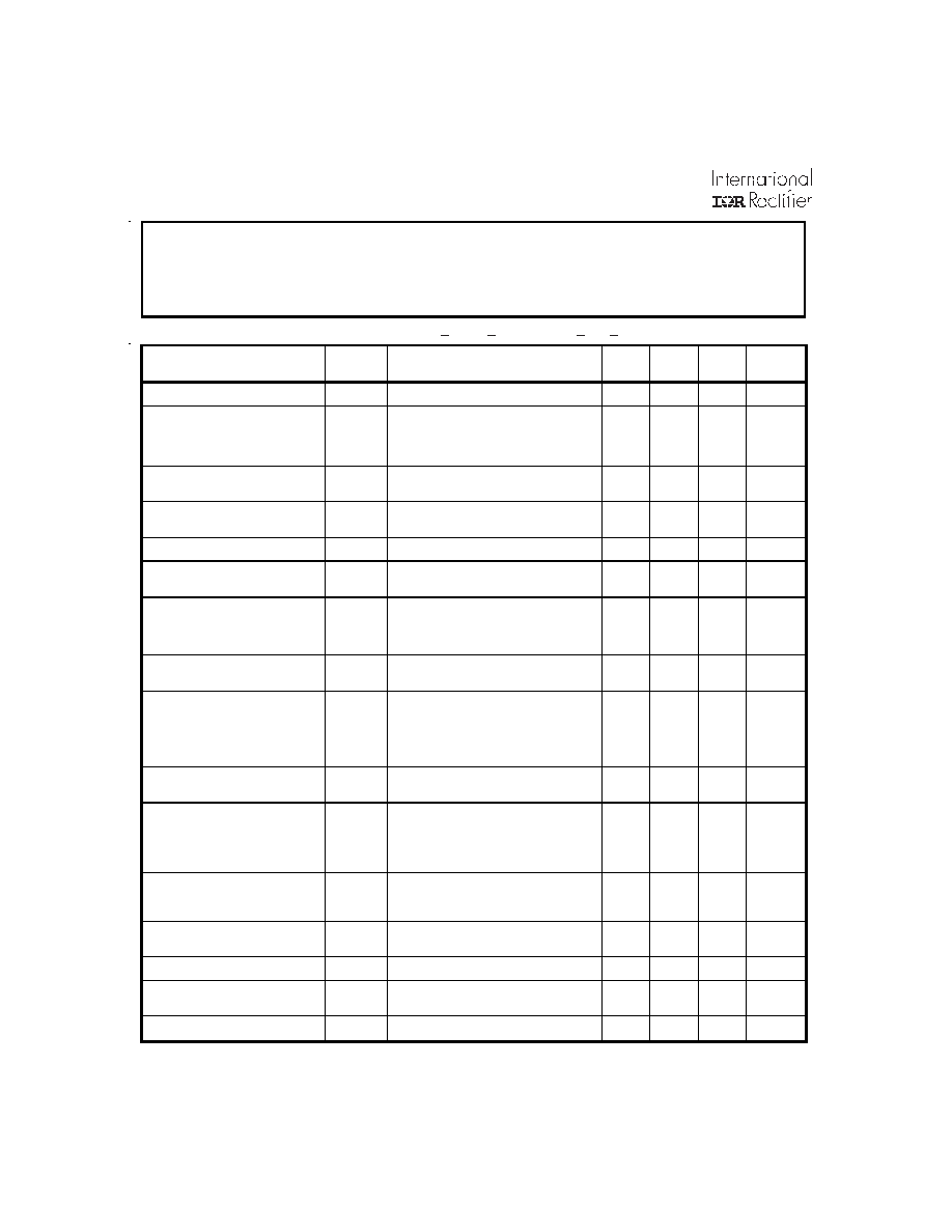
Specifications
Electrical Performance Characteristics
-55°C < T
CASE
< +125°C, 160V< V
IN
< 400V
unless otherwise specified.
For Notes to Specifications, refer to page 3
ABSOLUTE MAXIMUM RATINGS
Input Voltage
-0.5V to 500V
Soldering Temperature
300°C for 10 seconds
Case Temperature
Operating
-55°C to +125°C
Storage
-65°C to +135°C
Parameter
Group A
Subgroups
Test Conditions
Min
Nom
Max
Unit
INPUT VOLTAGE
Note
6
160 270 400 V
OUTPUT VOLTAGE
1
2, 3
VIN = 270 Volts, 100% Load
3.27
3.23
3.30
3.33
3.37
V
V
OUTPUT CURRENT
VIN = 160, 270, 400 Volts, Note 6
20 A
OUTPUT POWER
Note
6
66 W
MAXIMUM CAPACITIVE LOAD
4 Note
1
10,000
µfd
OUTPUT VOLTAGE
TEMPERATURE COEFFICIENT
VIN = 270 Volts, 100% Load - Note 1, 6
-0.015 +0.015
%/°C
OUTPUT VOLTAGE REGULATION
Line
Load
1, 2, 3
1, 2, 3
No Load, 50% Load, 100% Load
VIN = 160, 270, 400 Volts
-10.0
-35.0
+10.0
+35.0
mV
mV
OUTPUT RIPPLE VOLTAGE
1, 2, 3
VIN = 160, 270, 400 Volts, 100% Load,
BW = 10MHz
30
mVpp
INPUT CURRENT
No
Load
Inhibit
1
Inhibit
2
1
2, 3
1, 2, 3
1, 2, 3
VIN = 270 Volts
IOUT = 0
Pin 4 Shorted to Pin 2
Pin 12 Shorted to Pin 8
15.0
17.0
3.00
5.00
mA
mA
mA
mA
INPUT RIPPLE CURRENT
1, 2, 3
VIN = 270 Volts, 100% Load
B.W. = 10MHz
60
mApp
CURRENT LIMIT POINT
Expressed as a
Percentage
of Full Rated Load
1
2
3
VOUT = 90% VNOM
Note 5
115
105
125
125
115
140
%
%
%
LOAD FAULT POWER
DISSIPATION
Overload or Short Circuit
1, 2, 3
V
IN
= 270 Volts
30
W
EFFICIENCY
1, 2, 3
V
IN
= 270 Volts, 100% Load
72
74
%
SWITCHING FREQUENCY
1,
2,
3
500 550 600 KHz
ISOLATION
1
Input to Output or Any Pin to Case
(except Pin 3). Test @ 500VDC
100 M
MTBF
MIL-HDBK-217F, AIF @ TC = 40°C
300 KHrs
www.irf.com
3
AFL27003R3S
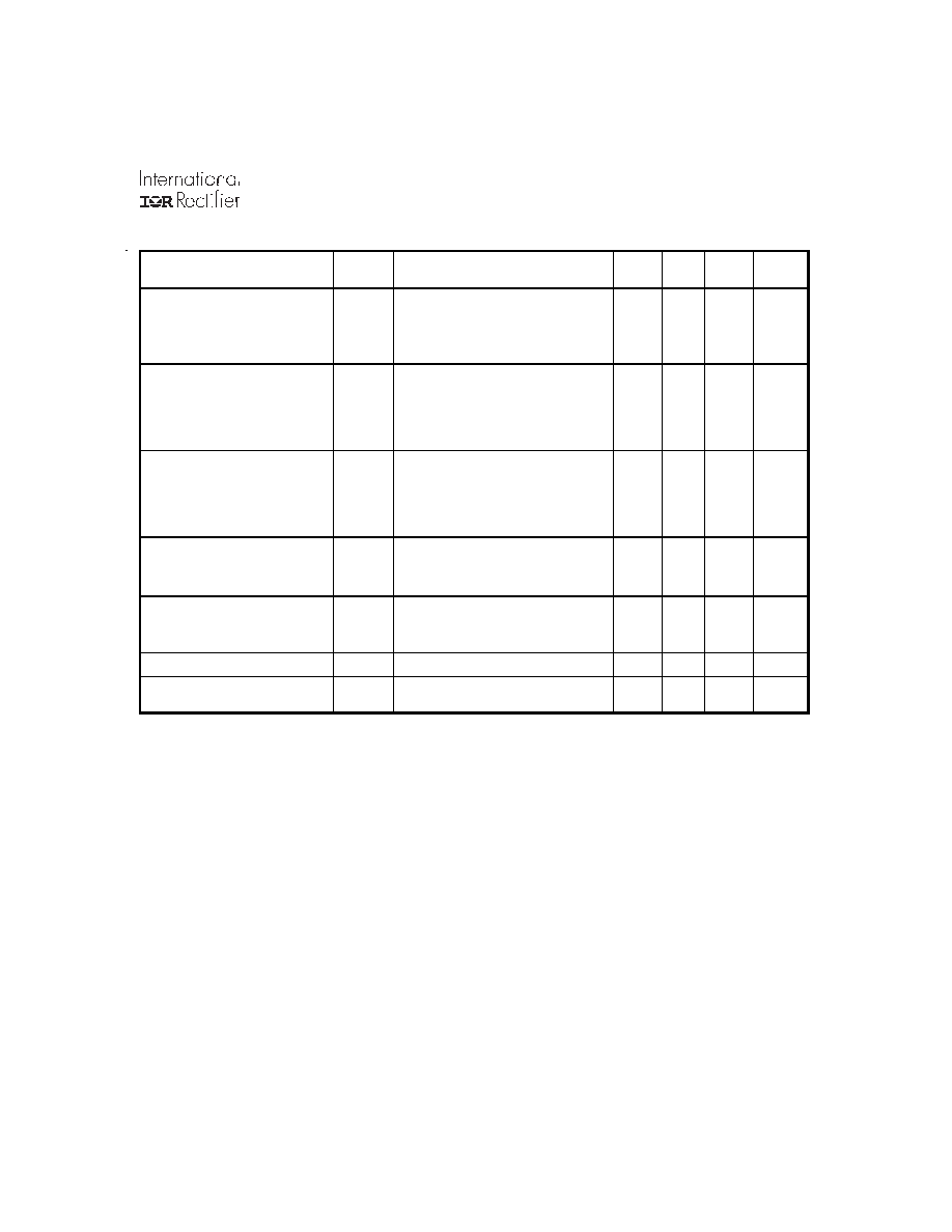
Elecrical Performance Characteristics
(Continued)
Notes to Specifications:
1.
Parameters not 100% tested but are guaranteed to the limits specified in the table.
2.
Recovery time is measured from the initiation of the transient to where V
OUT
has returned to within
±1% of V
OUT
at 50% load.
3.
Line transient transition time
100 µSec.
4.
Turn-on delay is measured with an input voltage rise time of between 100 and 500 volts per millisecond.
5.
Current limit point is that condition of excess load causing output voltage to drop to 90% of nominal.
6.
Parameter verified as part of another test.
7.
All electrical tests are performed with the remote sense leads connected to the output leads at the load.
8.
Load transient transition time
10 µSec.
9.
Enable inputs internally pulled high. Nominal open circuit voltage
4.0VDC.
Parameter
Group A
Subgroups
Test Conditions
Min
Nom
Max
Unit
ENABLE INPUTS (Inhibit Function)
Converter Off
Sink
Current
Converter
On
Sink
Current
1, 2, 3
1, 2, 3
Logical Low, Pin 4 or Pin 12
Note 1
Logical High, Pin 4 and Pin 12 - Note 9
Note 1
-0.5
2.0
0.8
100
50
100
V
µA
V
µA
SYNCHRONIZATION INPUT
Frequency Range
Pulse
Amplitude,
Hi
Pulse
Amplitude,
Lo
Pulse
Rise
Time
Pulse
Duty
Cycle
1, 2, 3
1, 2, 3
1, 2, 3
Note 1
Note 1
500
2.0
-0.5
20
700
10
0.8
100
80
KHz
V
V
nSec
%
LOAD TRANSIENT RESPONSE
Amplitude
Recovery
Amplitude
Recovery
4, 5, 6
4, 5, 6
4, 5, 6
4, 5, 6
Note 2, 8
Load Step 50%
100%
Load Step 10%
50%
-450
-450
450
200
450
400
mV
µSec
mV
µSec
LINE TRANSIENT RESPONSE
Amplitude
Recovery
Note 1, 2, 3
VIN Step = 160 400 Volts
-500
500
500
mV
µSec
TURN-ON CHARACTERISTICS
Overshoot
Delay
4, 5, 6
4, 5, 6
VIN = 160, 270, 400 Volts. Note 4
Enable 1, 2 on. (Pins 4, 12 high or open)
50
75
250
120
mV
mSec
LOAD FAULT RECOVERY
Same as Turn On Characteristics.
LINE REJECTION
MIL-STD-461, CS101, 30Hz to 50KHz
Note 1
60 70 dB
4
www.irf.com
AFL27003R3S
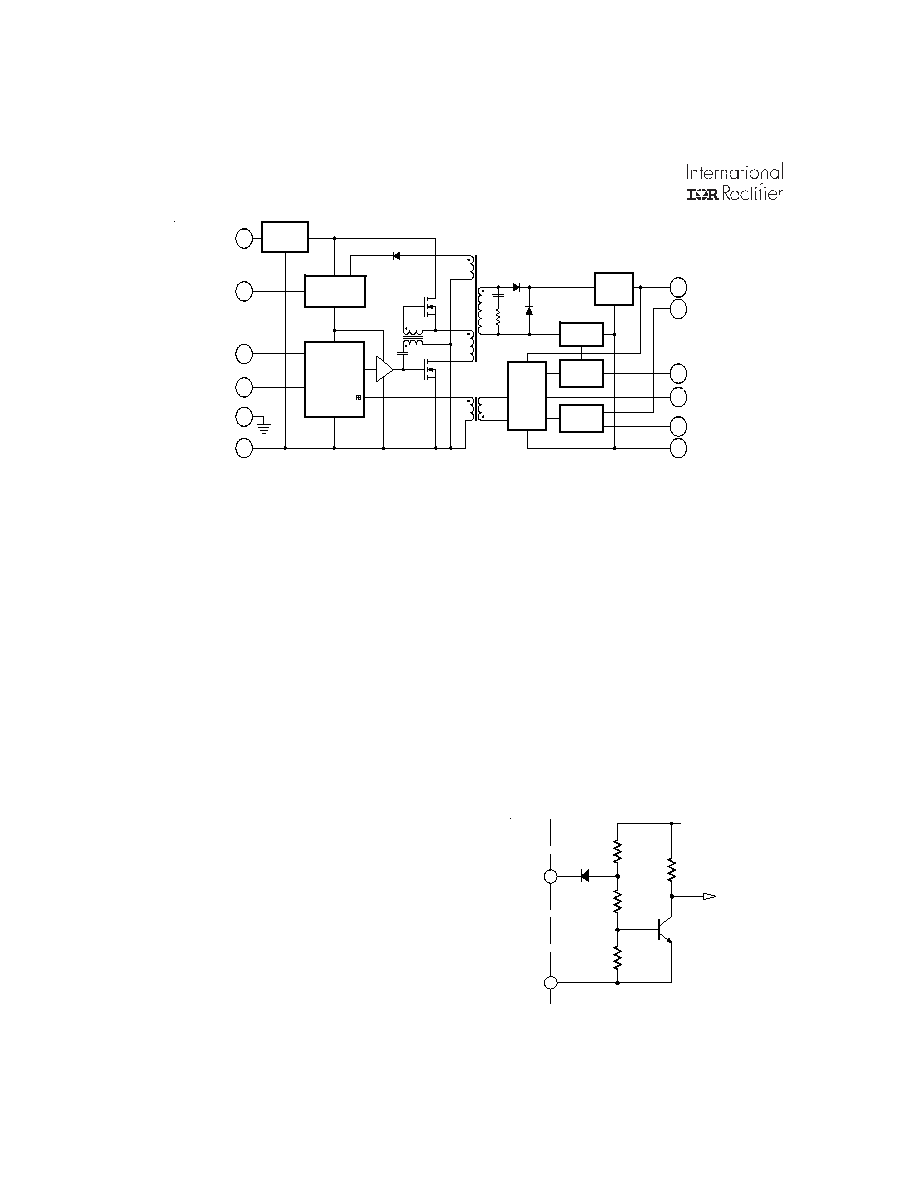
AFL27003R3S Circuit Description
Figure I. AFL Single Output Block Diagram
Connection of the + and - sense leads at a remotely locat-
led load permits compensation for resistive voltage drop
between the converter output and the load when they are
physically separated by a significant distance. This
connection allows regulation to the placard voltage at the
point of application.When the remote sensing features is
Figure II. Enable Input Equivalent Circuit
Pin 4 or
Pin 12
1N4148
100K
290K
150K
2N3904
+5.6V
Disable
Pin 2 or
Pin 8
not used, the sense leads should be connected to their
respective output terminals at the converter. Figure III.
illustrates a typical application.
Circuit Operation and Application Information
The AFL series of converters employ a forward switched
mode converter topology. (refer to Figure I.) Operation of
the device is initiated when a DC voltage whose magnitude
is within the specified input limits is applied between pins 1
and 2. If pin 4 is enabled (at a logical 1 or open) the primary
bias supply will begin generating a regulated housekeeping
voltage bringing the circuitry on the primary side of the
converter to life. Two power MOSFETs used to chop the
DC input voltage into a high frequency square wave, apply
this chopped voltage to the power transformer. As this
switching is initiated, a voltage is impressed on a second
winding of the power transformer which is then rectified and
applied to the primary bias supply. When this occurs, the
input voltage is shut out and the primary bias voltage
becomes exclusively internally generated.
The switched voltage impressed on the secondary output
transformer winding is rectified and filtered to provide the
converter output voltage. An error amplifier on the
secondary side compares the output voltage to a precision
reference and generates an error signal proportional to the
difference. This error signal is magnetically coupled through
the feedback transformer into the controller section of the
converter varying the pulse width of the square wave signal
driving the MOSFETs, narrowing the width if the output
voltage is too high and widening it if it is too low.
Remote Sensing
Inhibiting Converter Output
As an alternative to application and removal of the DC
voltage to the input, the user can control the converter
output by providing TTL compatible, positive logic signals
to either of two enable pins (pin 4 or 12). The distinction
between these two signal ports is that enable 1 (pin 4) is
referenced to the input return (pin 2) while enable 2 (pin 12)
is referenced to the output return (pin 8). Thus, the user
has access to an inhibit function on either side of the isolation
barrier. Each port is internally pulled "high" so that when
not used, an open connection on both enable
pins permits
normal converter operation. When their use is desired, a
logical "low" on either port will shut the
converter down.
ERROR
AMP
& REF
OUTPUT
FILTER
INPUT
FILTER
OUTPUT RETURN
DC INPUT
INPUT RETURN
CONTROL
1
2
4
3
5
6
SYNC INPUT
CURRENT
SENSE
+ SENSE
- SENSE
SENSE
AMPLIFIER
ENABLE 2
SHARE
SHARE
AMPLIFIER
7
11
10
9
12
8
+ OUTPUT
SYNC OUTPUT
ENABLE 1
CASE
PRIMARY
BIAS SUPPLY
www.irf.com
5
AFL27003R3S
high
l
evel of +2.0 volts. The sync output of another converter
which has been designated as the master oscillator provides
a convenient frequency source for this mode of operation.
When external synchronization is not required, the sync in
pin should be left unconnected thereby permitting the
converter to operate at its' own internally set frequency.
The sync output signal is a continuous pulse train set at
550
±50 KHz, with a duty cycle of 15 ±5%. This signal is
referenced to the input return and has been tailored to be
compatible with the AFL sync input port. Transition times
are less than 100 ns and the low level output impedance is
less than 50 ohms. This signal is active when the DC input
voltage is within the specified operating range and the
converter is not inhibited. This output has adequate drive
reserve to synchronize at least five additional converters.
A typical synchronization connection option is illustrated in
Figure III.
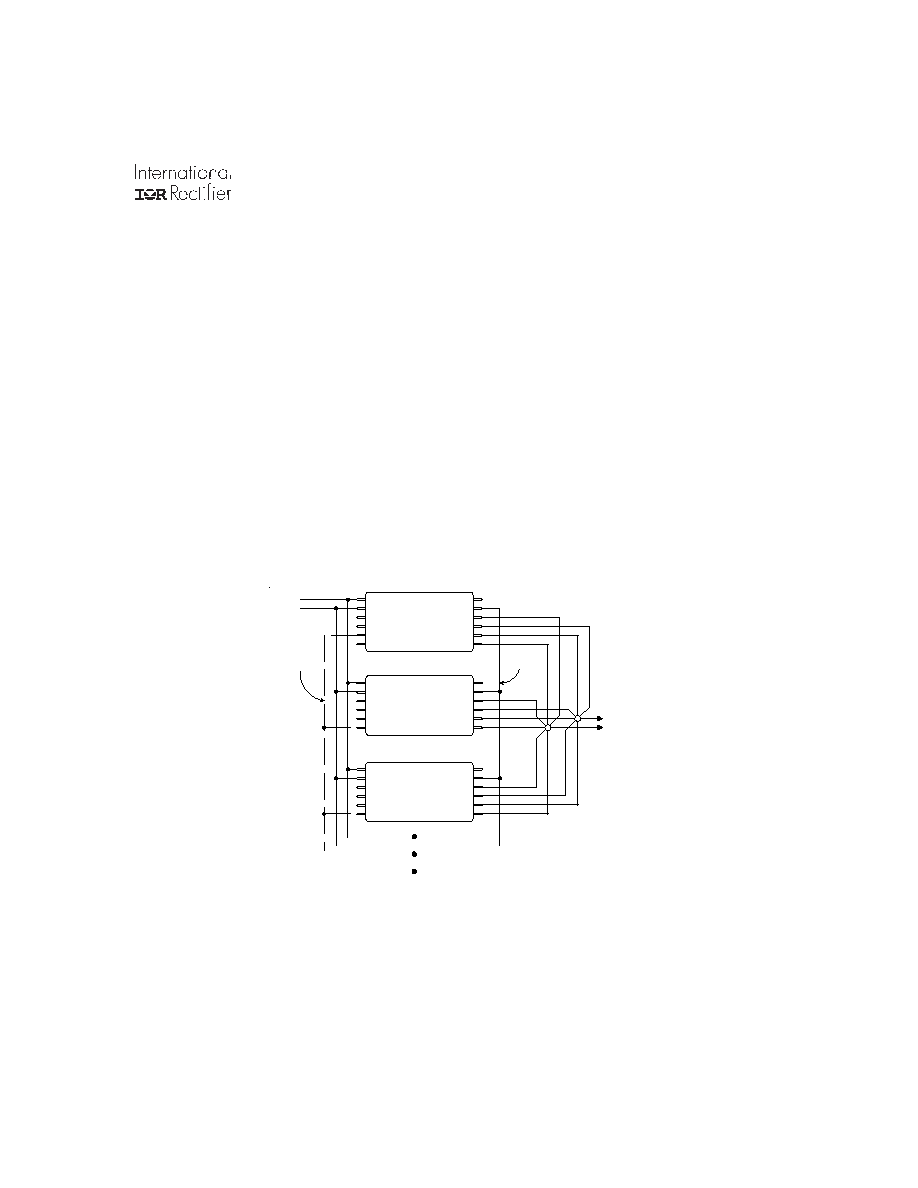
Figure III. Preferred Connection for Parallel Operation
Optional
Synchronization
Connection
Power
Input
(Other Converters)
Share Bus
1
6
AFL
7
12
- Sense
Enable 2
+ Vout
Return
+ Sense
Share
Vin
Rtn
Case
Enable 1
Sync Out
Sync In
1
6
AFL
7
12
- Sense
Enable 2
+ Vout
Return
+ Sense
Share
Vin
Rtn
Case
Enable 1
Sync Out
Sync In
1
6
AFL
7
12
- Sense
Enable 2
+ Vout
Return
+ Sense
Share
Vin
Rtn
Case
Enable 1
Sync Out
Sync In
to Load
AFL series operating in the parallel mode is that in
addition
to sharing the current, the stress induced by temperature
will also be shared. Thus if one member of a paralleled set
is operating at a higher case temperture, the current it pro-
vides to the load will be reduced as compensation for the
temperature induced stress on that device.
When operating multiple converters, system requirements
often dictate operation of the converters at a common
frequency. To accommodate this requirement, the AFL
series converters provide both a synchronization input and
output.
The sync input port permits synchronization of an AFL
converter to any compatible external frequency source
operating between 500 and 700 KHz. This input signal
should be referenced to the input return and have a 10% to
90% duty cycle. Compatibility requires transition times less
th an100 ns, maximum low level of +0.8 volts and a minimum
Figure III. illustrates the preferred connection scheme for
operation of a set of AFL converters with outputs operating
in parallel. Use of this connection permits equal sharing of
a load current exceeding the capacity of an individual AFL
among the members of the set. An important feature of the
Internally, these ports differ slightly in their function. In use,
a low on Enable 1 completely shuts down all circuits in the
converter while a low on Enable 2 shuts down the secondary
side while altering the controller duty cycle to near zero.
Externally, the use of either port is transparent to the user
save for minor differences in idle current. (See specification
table).
Synchronization of Multiple Converters
Parallel Operation-Current and Stress Sharing