 | ÐлекÑÑоннÑй компоненÑ: AFL27015D | СкаÑаÑÑ:  PDF PDF  ZIP ZIP |
AFL270XXD.pmd

09/11/02
www.irf.com
1
ADVANCED ANALOG
HIGH RELIABILITY
HYBRID DC/DC CONVERTERS
AFL270XXD SERIES
The AFL Series of DC/DC converters feature high power
density with no derating over the full military tempera-
ture range. This series is offered as part of a complete
family of converters providing single and dual output
voltages and operating from nominal +28 or +270 volt
inputs with output power ranging from 80 to 120 watts.
For applications requiring higher output power, indi-
vidual converters can be operated in parallel. The inter-
nal current sharing circuits assure equal current distri-
bution among the paralleled converters. This series in-
corporates Advanced Analog's proprietary magnetic
pulse feedback technology providing optimum dynamic
line and load regulation response. This feedback sys-
tem samples the output voltage at the pulse width modu-
lator fixed clock frequency, nominally 550 KHz. Multiple
converters can be synchronized to a system clock in the
500 KHz to 700 KHz range or to the synchronization
output of one converter. Undervoltage lockout, primary
and secondary referenced inhibit, soft-start and load
fault protection are provided on all models.
These converters are hermetically packaged in two en-
closure variations, utilizing copper core pins to mini-
mize resistive DC losses. Three lead styles are avail-
able, each fabricated with Advanced Analog's rugged
ceramic lead-to-package seal assuring long term
hermeticity in the most harsh environments.
Description
n
160 To 400 Volt Input Range
n
±
5,
±
12, and
±
15 Volts Outputs Available
n
High Power Density - up to 70 W / in3
n
Up To 100 Watt Output Power
n
Parallel Operation with Power Sharing
n
Low Profile (0.380") Seam Welded Package
n
Ceramic Feedthru Copper Core Pins
n
High Efficiency - to 87%
n
Full Military Temperature Range
n
Continuous Short Circuit and Overload
Protection
n
Output Voltage Trim
n
Primary and Secondary Referenced
Inhibit Functions
n
Line Rejection > 60 dB - DC to 50KHz
n
External Synchronization Port
n
Fault Tolerant Design
n
Single Output Versions Available
n
Standard Military Drawings Available
Features
AFL
270V Input, Dual Output
Manufactured in a facility fully qualified to MIL-PRF-
38534, these converters are available in four screening
grades to satisfy a wide range of requirements. The CH
grade is fully compliant to the requirements of MIL-H-
38534 for class H. The HB grade is processed and
screened to the class H requirement, but may not nec-
essarily meet all of the other MIL-PRF-38534 require-
ments, e.g., element evaluation and Periodic Inspection
(P.I.) not required. Both grades are tested to meet the
complete group "A" test specification over the full mili-
tary temperature range without output power deration.
Two grades with more limited screening are also avail-
able for use in less demanding applications. Varia-
tions in electrical, mechanical and screening can
be accommodated. Contact Advanced Analog for
special requirements.
PD - 94461B
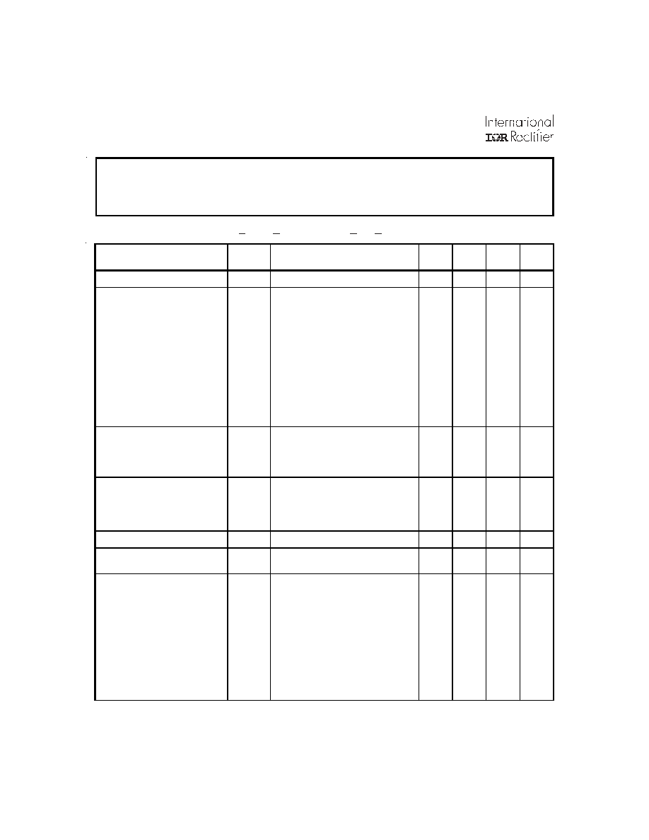
2
www.irf.com
AFL270XXD Series
Specifications
Static Characteristics -55°C < T
CASE
< +125°C, 160V< V
IN
< 400V
unless otherwise specified.
For Notes to Specifications, refer to page 4
ABSOLUTE MAXIMUM RATINGS
Input Voltage
-0.5V to 500V
Soldering Temperature
300°C for 10 seconds
Case Temperature
Operating -55°C to +125°C
Storage
-65°C to +135°C
Parameter
Group A
Subgroups
Test Conditions
Min
Nom
Max
Unit
INPUT VOLTAGE
Note
6
160
270
400
V
OUTPUT VOLTAGE
AFL27005D
AFL27012D
AFL27015D
AFL27005D
AFL27012D
AFL27015D
1
1
1
1
1
1
2, 3
2, 3
2, 3
2, 3
2, 3
2, 3
VIN = 270 Volts, 100% Load
Positive Output
Negative Output
Positive Output
Negative Output
Positive Output
Negative Output
Positive Output
Negative Output
Positive Output
Negative Output
Positive Output
Negative Output
4.95
-5.05
11.88
-12.12
14.85
-15.15
4.90
-5.10
11.76
-12.24
14.70
-15.30
5.00
-5.00
12.00
-12.00
15.00
-15.00
5.05
-4.95
12.12
-11.88
15.15
-14.85
5.10
-4.90
12.24
-11.76
15.30
-14.70
V
V
V
V
V
V
V
V
V
V
V
V
OUTPUT CURRENT
AFL27005D
AFL27012D
AFL27015D
VIN = 160, 270, 400 Volts - Notes 6, 11
Either Output
Either Output
Either Output
12.8
6.4
5.3
A
A
A
OUTPUT POWER
AFL27005D
AFL27012D
AFL27015D
Total of Both Outputs. Notes 6,11
80
96
100
W
W
W
MAXIMUM CAPACITIVE LOAD
Each Output Note 1
5,000
µ
fd
OUTPUT VOLTAGE
TEMPERATURE COEFFICIENT
VIN = 270 Volts, 100% Load - Notes 1, 6
-0.015
+0.015
%/°C
OUTPUT VOLTAGE REGULATION
Line
Load
Cross
AFL27005D
AFL27012D
AFL27015D
1, 2, 3
1, 2, 3
1, 2, 3
1, 2, 3
1, 2, 3
Note 10
No Load, 50% Load, 100% Load
VIN = 160, 270, 400 Volts.
VIN = 160, 270, 400 Volts. Note 12
Positive Output
Negative Output
Positive Output
Negative Output
Positive Output
Negative Output
-0.5
-1.0
-1.0
-8.0
-1.0
-5.0
-1.0
-5.0
+0.5
+1.0
+1.0
+8.0
+1.0
+5.0
+1.0
+5.0
%
%
%
%
%
%
%
%

www.irf.com
3
AFL270XXD Series
Static Characteristics
(Continued)
For Notes to Specifications, refer to page 4
Parameter
Group A
Subgroups
Test Conditions
Min
Nom
Max
Unit
OUTPUT RIPPLE VOLTAGE
AFL27005D
AFL27012D
AFL27015D
1, 2, 3
1, 2, 3
1, 2, 3
VIN = 160, 270, 400 Volts, 100% Load,
BW = 10MHz
60
80
80
mVpp
mVpp
mVpp
INPUT CURRENT
No
Load
Inhibit
1
Inhibit
2
1
2, 3
1, 2, 3
1, 2, 3
VIN = 270 Volts
IOUT = 0
Pin 4 Shorted to Pin 2
Pin 12 Shorted to Pin 8
10.00
12.00
3.00
5.00
mA
mA
mA
mA
INPUT RIPPLE CURRENT
AFL27005D
AFL27012D
AFL27015D
1, 2, 3
1, 2, 3
1, 2, 3
VIN = 270 Volts, 100% Load
60
70
80
mApp
mApp
mApp
CURRENT LIMIT POINT
Expressed as a Percentage
of Full Rated Load
1
2
3
VOUT = 90% VNOM , Current split
equally on positive and negative outputs.
Note 5
115
105
125
125
115
140
%
%
%
LOAD FAULT POWER
DISSIPATION
Overload or Short Circuit
1, 2, 3
V
IN
= 270 Volts
30
W
EFFICIENCY
AFL27005D
AFL27012D
AFL27015D
1, 2, 3
1, 2, 3
1, 2, 3
V
IN
= 270 Volts, 100% Load
78
82
83
82
85
87
%
%
%
ENABLE INPUTS (Inhibit Function)
Converter Off
Sink
Current
Converter
On
Sink
Current
1, 2, 3
1, 2, 3
Logical Low on Pin 4 or Pin 12
Note 1
Logical High on Pin 4 and Pin 12 - Note 9
Note 1
-0.5
2.0
0.8
100
50
100
V
µ
A
V
µ
A
SWITCHING FREQUENCY
1, 2, 3
500
550
600
KHz
SYNCHRONIZATION INPUT
Frequency Range
Pulse
Amplitude,
Hi
Pulse
Amplitude,
Lo
Pulse Rise Time
Pulse Duty Cycle
1, 2, 3
1, 2, 3
1, 2, 3
Note 1
Note 1
500
2.0
-0.5
20
700
10
0.8
100
80
KHz
V
V
nSec
%
ISOLATION
1
Input to Output or Any Pin to Case
(except Pin 3). Test @ 500VDC
100
M
DEVICE WEIGHT
Slight Variations with Case Style
85
gms
MTBF
MIL-HDBK-217F, AIF @ TC = 70°C
300
KHrs

4
www.irf.com
AFL270XXD Series
Dynamic Characteristics -55°C < T
CASE
< +125°C, V
IN
=270V
unless otherwise specified.
Notes to Specifications:
1.
Parameters not 100% tested but are guaranteed to the limits specified in the table.
2.
Recovery time is measured from the initiation of the transient to where Vout has returned to within
±
1% of Vout
at 50% load.
3.
Line transient transition time
100
µ
Sec.
4.
Turn-on delay is measured with an input voltage rise time of between 100 and 500 volts per millisecond.
5.
Current limit point is that condition of excess load causing output voltage to drop to 90% of nominal.
6.
Parameter verified as part of another test.
7.
All electrical tests are performed with the remote sense leads connected to the output leads at the load.
8.
Load transient transition time
10
µ
Sec.
9.
Enable inputs internally pulled high. Nominal open circuit voltage
4.0VDC.
10. Load current split equally between +Vout and -Vout.
11. Output load must be distributed so that a minimum of 20% of the total output power is being provided by one of
the outputs.
12. Cross regulation measured with load on tested output at 20% of maximum load while changing the load on
other output from 20% to 80%.
Parameter
Group A
Subgroups
Test Conditions
Min
Nom
Max
Unit
LOAD TRANSIENT RESPONSE
AFL2805D Amplitude
Either
Output Recovery
Amplitude
Recovery
AFL2812D Amplitude
Either
Output Recovery
Amplitude
Recovery
AFL2815D
Amplitude
Either
Output Recovery
Amplitude
Recovery
4, 5, 6
4, 5, 6
4, 5, 6
4, 5, 6
4, 5, 6
4, 5, 6
4, 5, 6
4, 5, 6
4, 5, 6
4, 5, 6
4, 5, 6
4, 5, 6
Note 2, 8
Load Step 50%
100%
Load Step 10%
50%
10%
50%
50%
10%
Load Step 50%
100%
Load Step 10%
50%
10%
50%
50%
10%
Load Step 50%
100%
Load Step 10%
50%
10%
50%
50%
10%
-450
-450
-750
-750
-750
-750
450
200
450
200
400
750
200
750
200
400
750
200
750
200
400
mV
µ
Sec
mV
µ
Sec
µ
Sec
mV
µ
Sec
mV
µ
Sec
µ
Sec
mV
µ
Sec
mV
µ
Sec
µ
Sec
LINE TRANSIENT RESPONSE
Amplitude
Recovery
Note 1, 2, 3
VIN Step = 160
400 Volts
-500
500
500
mV
µ
Sec
TURN-ON CHARACTERISTICS
Overshoot
Delay
4, 5, 6
4, 5, 6
VIN = 160, 270, 400 Volts. Note 4
Enable 1, 2 on. (Pins 4, 12 high or
open)
50
75
250
120
mV
mSec
LOAD FAULT RECOVERY
Same as Turn On Characteristics.
LINE REJECTION
MIL-STD-461D, CS101, 30Hz to
50KHz
Note 1
60 70 dB

www.irf.com
5
AFL270XXD Series
AFL270XXD Circuit Description
Figure I. AFL Dual Output Block Diagram
Figure II. Enable Input Equivalent Circuit
Pin 4 or
Pin 12
1N4148
100K
290K
150K
2N3904
+5.6V
Disable
Pin 2 or
Pin 8
Circuit Operation and Application Information
DC Input
Enable 1
Input
Filter
Sync Input
Primary
Bias Supply
Control
Sync Output
Input Return
Case
4
1
5
6
3
2
Error
Amp
& Ref
Output
Filter
Current
Sense
Output
Filter
Share
Amplifier
+ Output
Output Return
-Output
Share
Enable 2
Trim
7
8
9
11
12
10
The switched voltage impressed on the secondary output
transformer windings is rectified and filtered to provide the
positive and negative converter output voltages. An error
amplifier on the secondary side compares the positive out-
put voltage to a precision reference and generates an error
signal proportional to the difference. This error signal is
magnetically coupled through the feedback transformer into
the control section of the converter varying the pulse width
of the square wave signal driving the MOSFETs, narrowing
the pulse width if the output voltage is too high and widening
it if it is too low. These pulse width variations provide the
necessary corrections to regulate the magnitude of output
voltage within its' specified limits.
Because the primary portion of the circuit is coupled to the
secondary side with magnetic elements, full isolation from
input to output is maintained.
Although incorporating several sophisticated and useful
ancilliary features, basic operation of the AFL270XXDseries
can be initiated by simply applying an input voltage to pins 1
and 2 and connecting the appropriate loads between pins 7,
8, and 9. Of course, operation of any converter with high
power density should not be attempted before secure at-
tachment to an appropriate heat dissipator. (See Thermal
Considerations, page 7)
Inhibiting Converter Output
As an alternative to application and removal of the DC volt-
age to the input, the user can control the converter output
by providing TTL compatible, positive logic signals to either
of two enable pins (pin 4 or 12). The distinction between
these two signal ports is that enable 1 (pin 4) is referenced
to the input return (pin 2) while enable 2 (pin 12) is refer-
enced to the output return (pin 8). Thus, the user has
access to an inhibit function on either side of the isolation
barrier. Each port is internally pulled "high" so that when not
used, an open connection on both enable pins permits nor-
mal converter operation. When their use is desired, a logi-
cal "low" on either port will shut the converter down.
The AFL series of converters employ a forward switched
mode converter topology. (refer to Figure I.) Operation of
the device is initiated when a DC voltage whose magnitude
is within the specified input limits is applied between pins 1
and 2. If pins 4 and 12 are enabled (at a logical 1 or open)
the primary bias supply will begin generating a regulated
housekeeping voltage bringing the circuitry on the primary
side of the converter to life. Two power MOSFETs used to
chop the DC input voltage into a high frequency square
wave, apply this chopped voltage to the power transformer.
As this switching is initiated, a voltage is impressed on a
second winding of the power transformer which is then
rectified and applied to the primary bias supply. When this
occurs, the input voltage is excluded from the bias voltage
generator and the primary bias voltage becomes internally
generated.