 | –≠–ª–µ–∫—Ç—Ä–æ–Ω–Ω—ã–π –∫–æ–º–ø–æ–Ω–µ–Ω—Ç: AMA2805D | –°–∫–∞—á–∞—Ç—å:  PDF PDF  ZIP ZIP |

07/25/03
www.irf.com
1
ADVANCED ANALOG
RADIATION TOLERANT
DC/DC CONVERTERS
Description
n
5 Watts Output Power
n
Available in
±
5,
±
12 and
±
15 Volt Outputs
n
16 - 40 VDC Input Range (28 VDC Nominal)
n
Total Ionizing Dose > 25KRads (Si)
n
No SEE to LET > 60 MeV-cm
2
/mg
n
-55∞C to +125∞C Operating Range
n
Indefinite Short Circuit Protection
n
Flexible Mounting
n
Fully Isolated - Input to Output and to Case
n
Complimentary EMI Filter Available
n
Electrical Performance Similar to
ASA28XXD Series
Features
AMA
28V Input, Dual Output
The AMD28XXD series of DC/DC converter modules
has been specifically designed for operation in moder-
ate radiation environments supplementing the higher
radiation performance available in the Advanced Ana-
log ART2815T converter series. Environments pre-
sented to space vehicles operating in low earth orbits,
launch boosters, orbiting space stations and similar
applications requiring a low power, high performance
converter with moderate radiation hardness perfor-
mance will be optimally served by the AMA28XXD Se-
ries.
The AMA28XXD has been designed for high density
using chip and wire hybrid technology that complies
with the class H requirements of MIL-PRF-38534. Fin-
ished product will be fabricated in a facility fully quali-
fied to MIL-PRF-38534. The standard processing
adopted for the AMA28XXD is an enhancement of the
requirements of MIL-PRF-38534 for class H and in-
cludes element evaluation. Applicable generic lot quali-
fication test data including radiation performance can
be made available on request. Variations to the stan-
dard screening can be accomodated. Consult Ad-
vanced Analog for special requirements.
AMA28XXD SERIES
PD - 94692
The physical configuration of the AMA28XXD series
permits mounting directly to a heat conduction surface
without the necessity of signal leads penetrating the
heat sink surface. This package configuration permits
greater independence in mounting and more mechani-
cal security than traditional packages. Advanced
Analog's rugged ceramic seal pins are used exclusively
in the package thereby assuring long term hermeticity.
2
www.irf.com
AMA28XXD Series
Specifications
For Notes to Specifications, refer to page 4
Static Characteristics
-55∞C
TCASE
+125∞C, VIN=28 VDC
±
5%, C
L
=0,
unless otherwise specified.
Absolute Maximum Ratings
Input Voltage Range
-0.5V to +50VDC (Continuous), 80V (100ms)
Soldering Temperature
300∞C for 10 seconds
Storage Case Temperature
65∞C to +135∞C
Recommended Operating Conditions
Input Voltage Range
+16V to +40VDC
Output Power
Less than or equal to 5W
Operating Case Temperature
-55∞C to +125∞C
Parameter
Group A
Subgroups
Test Conditions
Min
Nom
Max
Unit
Input Voltage
16
28
40
V
Output Voltage
AMA2805D
AMA2812D
AMA2815D
AMA2805D
AMA2812D
AMA2815D
1
1
1
2, 3
2, 3
2, 3
Vin = 28 Volts, 20% load on
both outputs
±4.95
±11.88
±14.85
±4.90
±11.76
±14.70
±5.00
±12.00
±15.00
±5.05
±12.12
±15.15
±5.10
±12.24
±15.30
V
V
V
V
V
V
Output Current
1, 2
AMA2805D
AMA2812D
AMA2815D
1, 2, 3
1, 2, 3
1, 2, 3
Vin = 16, 28, 40 Volts
each output
each output
each output
200
83
67
800
333
267
mA
mA
mA
Output Power
1, 2
1, 2, 3
Vin = 28 Volts, 100% load
5
W
Output Ripple Voltage
1, 3
AMA2805D
AMA2812D
AMA2815D
1, 2, 3
1, 2, 3
1, 2, 3
Vin = 16, 28, 40 Volts
100% load
BW = 20 Hz to 2 MHz
200
200
290
mV
PP
mV
PP
mV
PP
Output Voltage Regulation
3
Line
AMA2805D
AMA2812D
AMA2815D
Load
AMA2805D
AMA2812D
AMA2815D
1, 2, 3
1, 2, 3
1, 2, 3
1, 2, 3
1, 2, 3
1, 2, 3
Vin = 16, 28, 40 Volts
Iout = 10, 50%, 100% load
±10
±10
±10
±10
±10
±10
±25
±50
±50
±50
±50
±50
mV
mV
mV
mV
mV
mV
Line

www.irf.com
3
AMA28XXD Series
Static Characteristics
(Continued)
-55∞C
TCASE
+125∞C, VIN=28 VDC
±
5%, C
L
=0,
unless otherwise specified.
For Notes to Specifications, refer to page 4
Parameter
Group A
Subgroups
Test Conditions
Min
Nom
Max
Unit
Cross Regulation
5
AMA2805D
AMA2812D
AMA2815D
1, 2, 3
1, 2, 3
1, 2, 3
Minimum 1.0 watt on both
outputs 20%-80% load
15
8
8
%
%
%
Input Current
No Load
Inhibit
1, 2, 3
1, 2, 3
Vin=28V,
Iout=0, Inhibit (pin 5)=open
Inhibit (pin 5) shorted to input
return (pin 7)
35
60
12
mA
mA
Input Ripple Current
3
AMA2805D
AMA2812D
AMA2815D
1, 2, 3
1, 2, 3
1, 2, 3
Vin = 16, 28, 40 Volts, 100%
load, BW = 20 Hz to 2 MHz
100
100
100
mA
PP
mA
PP
mA
PP
Efficiency
3
AMA2805D
AMA2812D
AMA2815D
AMA2805D
AMA2812D
AMA2815D
1, 3
1, 3
1, 3
2
2
2
100% load
66
71
71
60
68
68
%
%
%
%
%
%
Isolation
1
Input to output or any pin to
case (except pin 8) at 500Vdc
100
M
Capacitive Load
5, 6
AMA2805D
AMA2812D
AMA2815D
4
4
4
No effect on dc performance,
total for both outputs
500
200
200
uF
uF
uF
Short Circuit Power Dissipation
1, 2, 3
4
watts
MTBF
MIL-HDBK-217F, SF @ 35∞C
750
Khrs
Weight
32
g

4
www.irf.com
AMA28XXD Series
Dynamic Characteristics
-55∞C
TCASE
+125∞C, VIN=28 VDC
±
5%, C
L
=0,
unless otherwise specified.
Notes to Specifications
1.
Applicable to positive and negative outputs.
2.
Maximum combined output is 5 watts. 4 watts (max.) is available from either output (80%).
3.
Load current split equally between +V
OUT
and ≠V
OUT
.
4.
1.0 watt load on output under test, 1.0 watt to 4.0 watt load change on other output.
5.
Capacitive value may be any value from 0 to the maximum limit without compromising DC performance. A
capacitive load in excess of the maximum limit will not disturb loop stability but may interfere with the
operation of the load fault detection circuitry, appearing as a short circuit during turn-on.
6.
Parameter shall be tested as part of design characterization and after design or process changes.
Thereafter, parameters shall be guaranteed to the limit specified.
7.
Load step transition time between 2 and 10 microseconds.
8.
Recovery time is measured from initiation of the transient to where V
out
has returned to within
±
1% of V
out
at
50% load.
9.
Input step transient time between 1 and 10 microseconds.
10. Turn-on delay time measurement is for either a step application of power at the input or the removal of a
ground signal from the inhibit pin while power is applied to the input.
Parameter
Group A
Subgroups
Test Conditions
Min
Nom
Max
Unit
Short Circuit Recovery
6
4, 5, 6
0% load to 100% load
25
ms
Switching Frequency
3
4, 5, 6
100% load
500
550
600
KHz
Output Response To Step
Transient Load Changes
3, 7
4, 5, 6
4, 5, 6
Load step 50%Û 100%
Load step 0% Û 50%
-400
-800
+400
+800
mV pk
mv pk
Recovery Time, Step Transient
Load Changes
3, 7, 8
4, 5, 6
4, 5, 6
Load step 50%Û 100%
Load step 0% Û 50%
100
2000
µs
µs
Output Response Transient Step
Line Changes
3, 6, 9
AMA2805D
AMA2812D
AMA2815D
4, 5, 6
4, 5, 6
4, 5, 6
Input step 16 Û 40Vdc,
100% load
-550
-750
-750
+550
+750
+750
mV pk
mV pk
mv pk
Recovery Time Transient Step
Line Changes
3, 6, 9
4, 5, 6
Input step 16 40Vdc,
100% load
1200
µs
Turn On Overshoot
3, 10
4, 5, 6
4, 5, 6
0% load
100% load
600
400
mV pk
mV pk
Turn On Delay
3, 10
4, 5, 6
0% load to 100% load
25
ms
www.irf.com
5
AMA28XXD Series
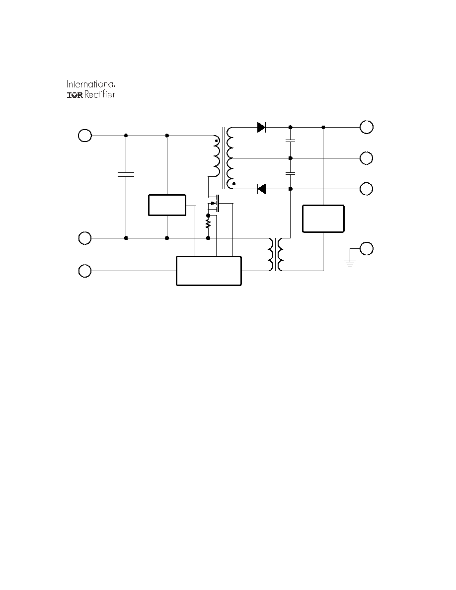
AMA28XXD Block Diagram
Application Information
Inhibit Function
Connecting the enable input (Pin 5) to input common
(Pin 7) will cause the converter to shut down. It is
recommended that the enable pin be driven by an
open collector device capable of sinking at least 400
µ
A of current. The open circuit voltage of the inhibit
input is 10.0 +1 V
DC
.
An optional EMI filter is available (ASF461 or AFH461)
will reduce the input ripple current to levels below the
limits imposed by MIL-STD-461 CE03.
EMI Filter
C o n tro lle r
E rror
A m plifier
1
2
8
6
7
5
C as e
R eturn
+ O u tput
E na ble
R eturn
+ Input
3
-O utput
C S
H o u se k e e p in g
S u p p ly
Thermal Considerations
Irrespective of the fact that the AMA28XXD series
of converters are relatively low power devices and
are designed to provide efficient voltage conver-
sion, there will be some heat generated during nor-
mal operation. To avoid a continuous thermal rise
that may eventually exceed the maximum case tem-
perature rating and to maintain a safe operating
environment for the internal components, these
converters should be attached to a heat conduct-
ing surface allowing a continuous flow of the heat
away from the base plate. This becomes more im-
portant when operating in the near vacuum envi-
ronment of space which provides no alternate heat
radiating path.