 | –≠–ª–µ–∫—Ç—Ä–æ–Ω–Ω—ã–π –∫–æ–º–ø–æ–Ω–µ–Ω—Ç: AMR2812S | –°–∫–∞—á–∞—Ç—å:  PDF PDF  ZIP ZIP |

07/25/03
www.irf.com
1
ADVANCED ANALOG
RADIATION TOLERANT
DC/DC CONVERTERS
Description
n
30 Watts Output Power
n
Available in 3.3, 5, 12 and 15 Volt Outputs
n
18 - 40 VDC Input Range (28 VDC Nominal)
n
Total Ionizing Dose > 25KRads (Si)
n
No SEE to LET > 60 MeV-cm
2
/mg
n
-55∞C to +125∞C Operating Range
n
Indefinite Short Circuit Protection
n
External Synchronization
n
Shutdown from External Signal
n
Flexible Mounting
n
Fully Isolated - Input to Output and to Case
n
Complimentary EMI Filter Available
n
Electrical Performance Similar to
ATR28XXS Series
Features
AMR
28V Input, Single Output
The AMR28XXS series of DC/DC converter modules
has been specifically designed for operation in moder-
ate radiation environments supplementing the higher
radiation performance available in the Advanced Ana-
log ART2815T converter series. Environments pre-
sented to space vehicles operating in low earth orbits,
launch boosters, orbiting space stations and similar
applications requiring a low power, high performance
converter with moderate radiation hardness perfor-
mance will be optimally served by the AMR28XXS Se-
ries.
The AMR28XXS has been designed for high density
using chip and wire hybrid technology that complies
with the class H requirements of MIL-PRF-38534. Fin-
ished product are fabricated in a facility fully qualified
to MIL-PRF-38534. The standard processing adopted
for the AMR2805S meets the requirements of MIL-PRF-
38534 for class H but with enhanced screening steps
and includes element evaluation. Applicable generic
lot qualification test data including radiation perfor-
mance can be made available on request. Consult
Advanced Analog for special requirements.
AMR28XXS SERIES
PD - 94691
The physical configuration of the AMR28XXS series
permits mounting directly to a heat conduction surface
without the necessity of signal leads penetrating the
heat sink surface. This package configuration permits
greater independence in mounting and more secure
mechanical attachment than traditional radially leaded
packages. Advanced Analog's rugged ceramic seal
pins are used exclusively in the package thereby as-
suring long term hermeticity.

2
www.irf.com
AMR28XXS Series
Specifications
For Notes to Specifications, refer to page 4
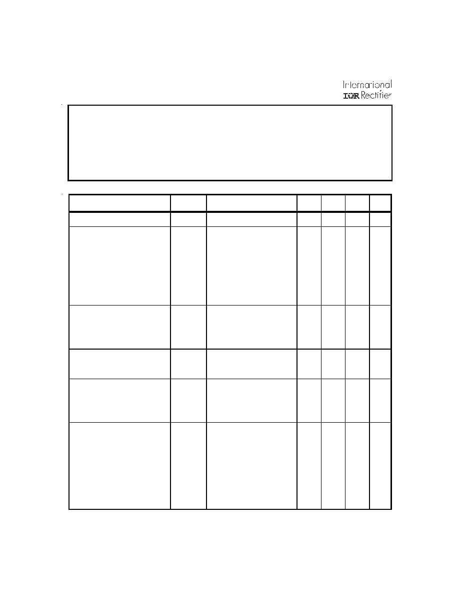
Parameter
Group A
Subgroups
Test
Conditions
Min
Nom
Max
Unit
Input Voltage
16
28
40
V
Output Voltage
AMR2803R3S
AMR2805S
AMR2812S
AMR2815S
AMR2803R3S
AMR2805S
AMR2812S
AMR2815S
1
1
1
1
2, 3
2, 3
2, 3
2, 3
Iout=0
3.25
4.95
11.88
14.85
3.20
4.90
11.70
14.60
3.30
5.00
12.00
15.00
3.35
5.05
12.12
15.15
3.40
5.10
12.30
15.40
V
V
V
V
V
V
V
V
Output Current
1
AMR2803R3S
AMR2805S
AMR2812S
AMR2815S
1, 2, 3
1, 2, 3
1, 2, 3
1, 2, 3
Vin = 18, 28, 40 Volts
7500
6000
2500
2000
mA
mA
mA
mA
Output Power
AMR2803R3S
All Others
1, 2, 3
1, 2, 3
100% load
25
30
W
W
Output Ripple Voltage
2
AMR2803R3S
AMR2805S
AMR2812S
AMR2815S
1, 2, 3
1, 2, 3
1, 2, 3
1, 2, 3
Vin = 18, 28, 40 Volts
BW = 20 Hz to 2 MHz
60
60
60
75
mV
PP
mV
PP
mV
PP
mV
PP
Output Voltage Regulation
3
L
ine AMR2803R3S
AMR2805S
AMR2812S
AMR2815S
L
oad AMR2803R3S
AMR2805S
AMR2812S
AMR2815S
1, 2, 3
1, 2, 3
1, 2, 3
1, 2, 3
1, 2, 3
1, 2, 3
1, 2, 3
1, 2, 3
Vin = 18, 28, 40 Volts
Iout = 0, 50%, and 100% load
±10
±10
±30
±40
±10
±10
±50
±50
±30
±30
±60
±75
±50
±50
±120
±150
mV
mV
mV
mV
mV
mV
mV
mV
Static Characteristics
-55∞C
TCASE
+125∞C, VIN=28 VDC
±
5%, C
L
=0,
unless otherwise specified.
Absolute Maximum Ratings
Input Voltage Range
-0.5V to +50VDC (Continuous), 80V (100ms)
Soldering Temperature
300∞C for 10 seconds
Storage Case Temperature
65∞C to +135∞C
Recommended Operating Conditions
Input Voltage Range
+16V to +40VDC
Output Power
Less than or equal to 30W
Operating Case Temperature
-55∞C to +125∞C

www.irf.com
3
AMR28XXS Series
Static Characteristics
(Continued)
-55∞C
TCASE
+125∞C, VIN=28 VDC
±
5%, C
L
=0, unless otherwise specified.
For Notes to Specifications, refer to page 4
Parameter
Group A
Subgroups
Test
Conditions
Min
Nom
Max
Unit
Input Current
No Load
AMR2803R3S
AMR2805S
AMR2812S
AMR2815S
Inhibited
All
1, 2, 3
1, 2, 3
1, 2, 3
1, 2, 3
1, 2, 3
Iout=0, Inhibit =open
Inhibit shorted to input return
20
20
20
20
8
50
50
75
100
18
mA
mA
mA
mA
mA
Input Ripple Current
2
1, 2, 3
Vin = 16, 28, 40 Volts, 100%
load, BW = 20 Hz to 2 MHz
50
mA
PP
Efficiency
AMR2803R3S
AMR2805S
AMR2812S
AMR2815S
AMR2803R3S
AMR2805S
AMR2812S
AMR2815S
1
1
1
1
2, 3
2, 3
2, 3
2, 3
100% load
74
76
80
79
70
72
75
75
%
%
%
%
%
%
%
%
Isolation
1
Input to output or any pin to case
(except case ground pin) at
500Vdc
100
M
Capacitive Load
4, 5
4
No effect on dc performance
500
µF
Short Circuit Power Dissipation
1, 2, 3
19
watts
Switching Frequency
4, 5, 6
100% load
500
550
600
KHz
Sync Frequency Range
4, 5, 6
100% load
500
700
KHz
MTBF
MIL-HDBK-217F, N2
SF @ Tc = 35∞C
940
Khrs
Weight
68
g

4
www.irf.com
AMR28XXS Series
Dynamic Characteristics
-55∞C
TCASE
+125∞C, VIN=28 VDC
±
5%, C
L
=0, unless otherwise specified.
1 Parameter guaranteed by line and load regulation tests.
2 Bandwidth guaranteed by design. Tested for 20 KHz to 2 MHz.
3 Output voltage measured at load with remote sense leads connected across load.
4 Capacitive load may be any value from 0 to the maximum limit without compromising dc performance. A capacitive load in excess of
the maximum limit will not disturb loop stability but may interfere with the operation of the load fault detection circuitry, appearing
as a short circuit during turn on.
5 Parameter shall be tested as part of design characterization and after design or process changes. Parameters shall be guaranteed
to the limit specified in Electrical Specifications.
6 Load step transition time between 2 and 10 microseconds.
7 Recovery time is measured from the initiation of the transient to where V
OUT
has returned to within ±1 % of V
OUT
at 50 percent load.
8 Input step transition time between 2 and 10 microseconds.
9 Turn on delay time measurement is for either a step application of power at the input or the removal of a ground signal from the
inhibit pin
while power is applied to the input.
Notes to Specifications
Parameter
Group A
Subgroups
Test Conditions
Min
Nom
Max
Unit
Output Response To Step
Transient Load Changes
7
AMR2803R3S
AMR2805S
AMR2812S
AMR2815S
AMR2803R3S
AMR2805S
AMR2812S
AMR2815S
4, 5, 6
4, 5, 6
4, 5, 6
4, 5, 6
4, 5, 6
4, 5, 6
Load step 50%Û 100%
Load step 8% Û 50%
-500
-500
-800
-1000
-500
-500
-1000
-1000
+500
+500
+800
+1000
+500
+500
+1000
+1000
mV
pk
mV
pk
mV
pk
mV
pk
mV
pk
mV
pk
mV
pk
mV
pk
Recovery Time, Step Transient
Load Changes
7, 8
4, 5, 6
Load step 50%Û 100% or
Load step 8% Û 50%
200
µs
Output Response Transient Step
Line Changes
5, 9
AMR2803R3S
AMR2805S
AMR2812S
AMR2815S
4, 5, 6
4, 5, 6
4, 5, 6
4, 5, 6
Input step from/to 18 to 40Vdc,
100% load
-500
-500
-1200
-1500
+500
+500
+1200
+1500
mV
pk
mV
pk
mV
pk
mV
pk
Recovery Time Transient Step
Line Changes
5, 8, 9
4, 5, 6
Input step from/to 18 to 40Vdc,
100% load
10
ms
Turn On Overshoot
AMR2803R3S
AMR2805S
AMR2812S
AMR2815S
4, 5, 6
4, 5, 6
4, 5, 6
4, 5, 6
0% load to 100% load
500
500
800
1000
mV
pk
mV
pk
mV
pk
mV
pk
Turn On Delay
10
4, 5, 6
0% load to 100% load
25
ms
Short Circuit Recovery
5, 10
4, 5, 6
25
ms

www.irf.com
5
AMR28XXS Series
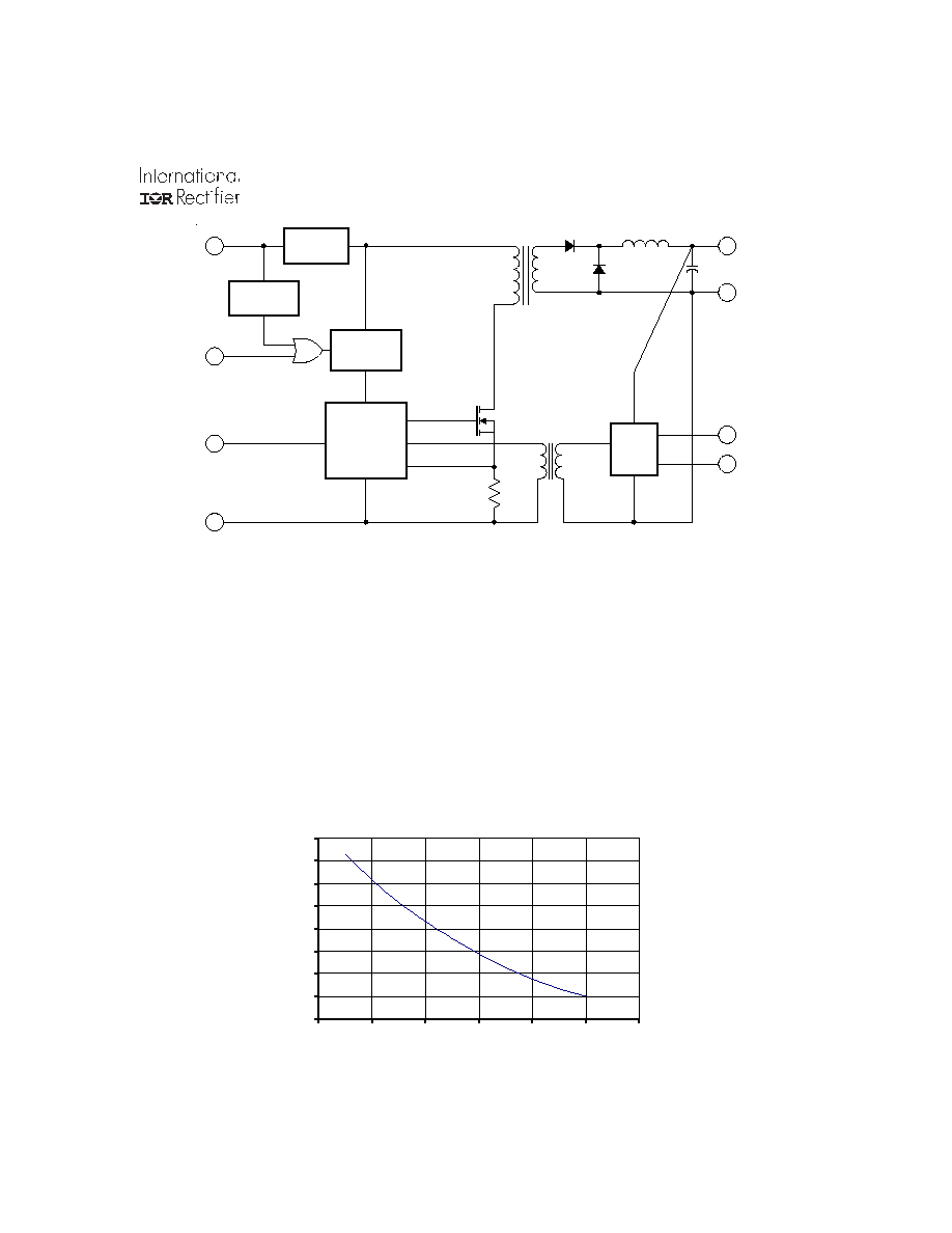
AMR28XXS Block Diagram
Application Information
Inhibit Function
EMI Filter
Device Synchronization
8
7
+ V o ut
R e turn
P ulse W id th
M o du la tor
P rim ary
H o u seke ep in g
S up p ly
E M I
F ilte r
U n d er-V o lta ge
D e tector
1
3
1 0
2
+ Inp u t
E na b le
S ync
Inp ut
R e turn
E rro r
A m p &
R e f
9
6
+ S e nse
-S e nse
F B
C S
D riv e
Connecting the inhibit input to input common will
cause the converter to shut down. It is recommended
that the inhibit pin be driven by an open collector
device capable of sinking at least 400
µ
A of current.
The open circuit voltage of the inhibit input is 10.0 +1
V
DC
.
An optional EMI filter is available (AFH461) that will
reduce the input ripple current to levels below the
limits imposed by MIL-STD-461 CE03.
When multiple DC/DC converters are utilized in a
single system, significant low frequency noise may
be generated due to a small difference in the switch-
ing frequency of the converters (beat frequency
noise). Because of the low frequency nature of this
noise (typically less than 10 KHz), it is difficult to
filter out and may interfere with proper operation of
sensitive systems (communication, radar or telem-
etry). Advanced Analog provides synchronization
of multiple AMR type converters to match switching
frequency of the converter to the frequency of the
system clock, thus eliminating this type of noise.
MTBF vs Case Temperature for AMR2803R3S
0.00E+00
2.00E+05
4.00E+05
6.00E+05
8.00E+05
1.00E+06
1.20E+06
1.40E+06
1.60E+06
0
20
40
60
80
100
120
Case Temperature, deg C
MTBF
