 | –≠–ª–µ–∫—Ç—Ä–æ–Ω–Ω—ã–π –∫–æ–º–ø–æ–Ω–µ–Ω—Ç: ATR2815SF | –°–∫–∞—á–∞—Ç—å:  PDF PDF  ZIP ZIP |

10/29/02
www.irf.com
1
ADVANCED ANALOG
HYBRID-HIGH RELIABILITY
DC/DC CONVERTERS
ATR28XXD SERIES
Description
n
16 to 40 VDC Input Range (28 VDC Nominal)
n
±
12V and
±
15V Outputs Available
n
Indefinite Short Circuit and Overload
Protection
n
35 W/in
3
Power Density
n
30 Watt Output Power
n
Fast Loop Response for Superior Transient
Characteristics
n
Operating Temperature Range from -55∞C to
+125∞C
n
Popular Industry Standard Pin-Out
n
Resistance Seam Welded Case for Superior
Long Term Hermeticity
n
Ceramic Feed-thru Pins
n
External Synchronization
n
High Efficiency
n
Shutdown from External Signal
n
Military Screening
Features
ATR
28V Input, Dual Output
The advanced feedback design provides fast loop re-
sponse for superior line and load transient character-
istics and offers greater reliability and radiation toler-
ance than devices incorporating optical feedback cir-
cuits.
Three standard temperature grades are offered with
screening options. Refer to Part Number section. They
can be provided in a standard plug-in package for PC
mounting or in a flanged package for more severe en-
vironments.
These converters are manufactured in a facility certi-
fied to MIL-PRF-38534. All processes used to manu-
facture these converters have been qualified to enable
Advanced Analog to deliver compliant devices.
Four screening grades are available to satisfy a wide
range of requirements. The CH grade converters are
fully compliant to MIL-PRF-38534 for class H. The HB
grade converters are processed to full class H screen-
ing but do not have class H element evaluation as re-
quired by MIL-PRF-38534. Both grades are fully tested
and operate over the full military temperature range
without derating of output power. The ES version is a
full temperature device without the full class H or ele-
ment evaluation. The non-suffix device is a low cost
limited temperature range option. Variations in
electrical, mechanical and screening can be ac-
commodated.
Extensive computer simulation using complex
modeling enables rapid design modification to
be provided. Contact Advanced Analog with spe-
cific requirements.
The ATR28XXD Series of DC/DC converters feature
high power density and an extended temperature range
for use in military and industrial applications. Designed
to MIL-STD-704D input requirements, these devices
have nominal 28VDC inputs with ±12V and ±15V dual
outputs to satisfy a wide range of requirements. The
circuit design incorporates a pulse width modulated
single forward topology operating in the feed-forward
mode at a nominal switching frequency of 550KHz.
Input to output isolation is achieved through the use of
transformers in the forward and feedback circuits.
PD - 94550

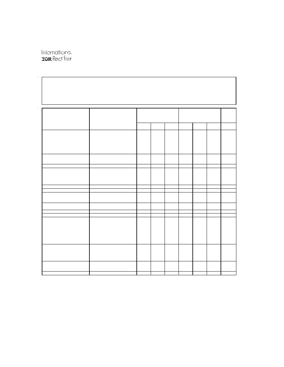
2
www.irf.com
ATR28XXD Series
Specifications
T
CASE
= -55∞C to +85∞C, V
IN
= +28V
±
5% unless otherwise specified
ABSOLUTE MAXIMUM RATINGS
Input Voltage -0.5V to 50VDC
Power Output Internally limited, 36W typical
Soldering 300
∞
C for 10 seconds
Temperature Range
1
Recommended Operating -55
∞
C to +85
∞
C
Maximum Operating -55
∞
C to +115
∞
C
Storage -65
∞
C to +135
∞
C
ATR2812D
ATR2815D
PARAMETER
Condition
-55
∞
C
TC
+85
∞
C, V
IN
= 28 V
DC
±
5%, CL=0, unless otherwise
specified
Min Typ Max Min Typ Max Units
STATIC
CHARACTERISTICS
OUTPUT
V
IN
= 16 to 40 V
DC
Voltage
I
OUT
= 0 to Full Load
±
11.76
±
12.00
±
12.24
±
14.70
±
15.00
±
15.30
V
DC
Current
5
0.0
±
1.25
0.0
±
1.0
A
DC
Ripple
Full Load, 20KHz to 2MHz
40
85
40
85
mV p-p
Accuracy
T
CASE
= 25
∞
C, Full Load
±
11.88
±
12.00
±
12.12
±
14.85
±
15.00
±
15.15
V
DC
Power
1
30 30 W
REGULATION
Line
Load
V
IN
= 16 to 40 V
DC
I
OUT
= 0 to Full Load
75
120
75
150
mV
mV
CROSS REGULATION
6
V
IN
= 16, 28, and 40 V
DC
±
5
±
5
%
INPUT
Voltage Range
Current
Ripple Current
No Load, pin 2 = open
Inhibited, pin 2 tied to pin 10
Full Load
16.0
28.0
25
40.0
75
18
50
16.0
28.0
25
40.0
75
18
50
V
DC
mA
DC
mA
DC
mA p-p
EFFICIENCY
Full Load T
C
= +25
∞
C
82 82 %
ISOLATION
Input to output @500 V
DC
100 100 M
CAPACITIVE LOAD
No effect on performance
T
C
= +25
∞
C (total for both outputs)
100 100
µ
F
Load Fault Power Dissipation
Short Circuit
Overload, T
C
= +25
∞
C
9
14
9
14
W
W
Switching Frequency
I
OUT
=
Full
Load
500 600
500 600
KHz
SYNC Frequency Range
7
500 700
500 700
KHz
DYNAMIC
CHARACTERISTICS
Step
Load
Changes
Output
Transient
Recovery
2
50% Load to
100% Load
No Load to 50% Load
50% Load to 100% Load
No Load to 50% Load
50% Load to No Load
±
100
±
250
25
500
3
±
100
±
250
25
500
3
mVpk
mVpk
µ
s
µ
s
ms
Step Line Changes
Output
Transient
Recovery
2
Input step 16 to 40 V
DC
Input step 40 to 16 V
DC
Input step 16 to 40 V
DC
Input step 40 to 16 V
DC
±
180
-600
5
5
±
180
-600
5
5
mVpk
mVpk
ms
ms
TURN-ON
Overshoot
Delay
3
V
IN
= 16 to 40 V
DC
I
OUT
= O and Full Load
0
14
600
25
0
14
600
25
mVpk
ms
Load Fault Recovery
V
IN
= 16 to 40 V
DC
14
25 14
25 ms
Notes to Specifications
1. Above +85
∞
C case temperature, derate output power linearly to 0 at +115
∞
C case.
2. Recovery time is measured from the initiation of the input transient to where V
OUT
has returned to within
±
1% of V
OUT
at 50% load.
3. Turn-on delay time measurement is for either an application of power at the input or a signal at the inhibit pin.
4. Load current split equally between +V
OUT
and ≠V
OUT
.
5. Up to 90% of Full Power is available from either output provided. The total power output does not exceed 30 watts.
6. 3W load on output under test, 3W to 27W on other output.
7. Sync. Input signal: V
IL
= -0.5V Min, V
IN
= 2.5V Min, 10% to 90% duty cycle,
0.8V Max 11.5V Max
www.irf.com
3
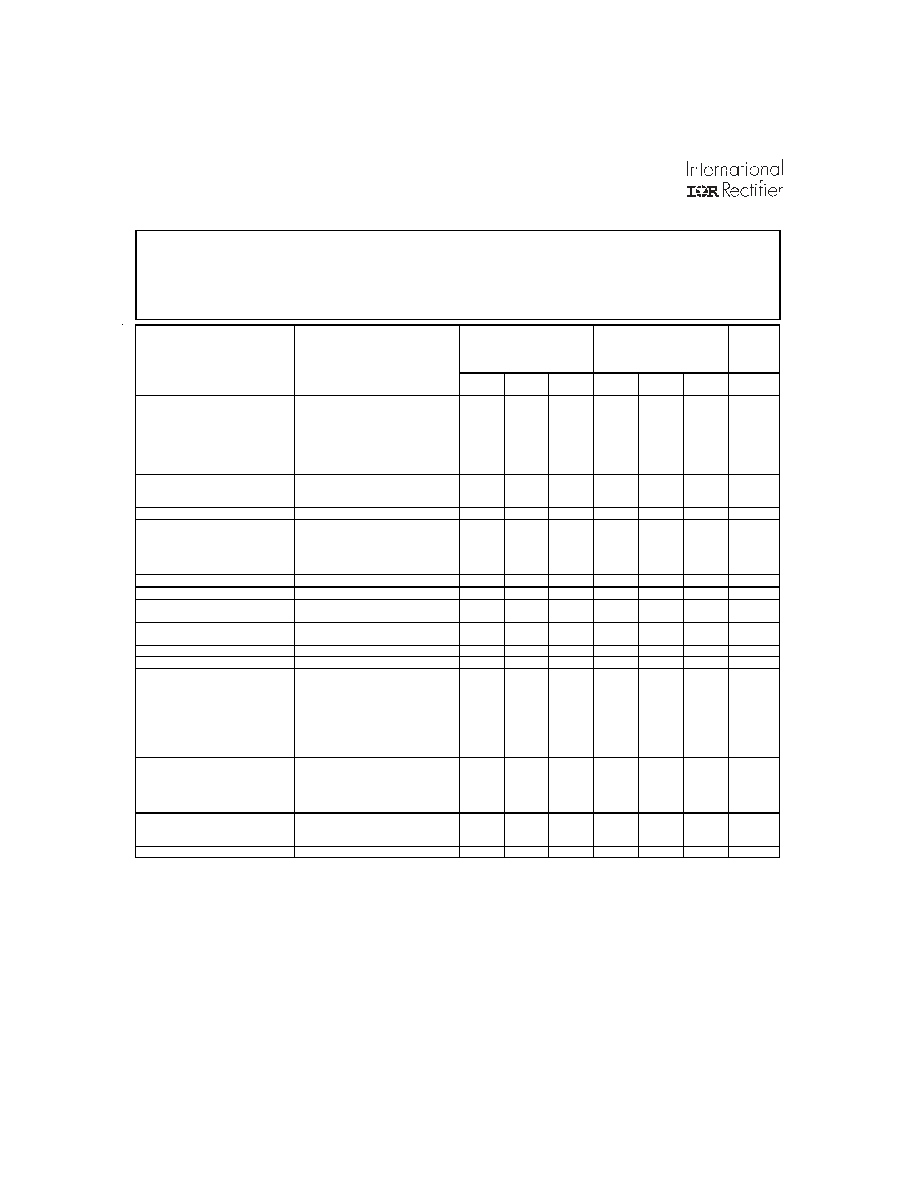
ATR28XXD Series
T
CASE
= -55∞C to +125∞C, V
IN
= +28V
±
5% unless otherwise specified
ABSOLUTE MAXIMUM RATINGS
Input Voltage -0.5V to 50VDC
Power Output Internally limited, 36W typical
Soldering 300
∞
C for 10 seconds
Temperature Range
1
Recommended Operating -55
∞
C to +125
∞
C
Maximum Operating -55
∞
C to +135
∞
C
Storage -65
∞
C to +135
∞
C
Notes to Specifications
1. Above +125
∞
C case temperature, derate output power linearly to 0 at +135
∞
C case.
2. Recovery time is measured from the initiation of the input transient to where V
OUT
has returned to within
±
1% of V
OUT
at 50% load.
3. Turn-on delay time measurement is for either an application of power at the input or a signal at the inhibit pin.
4. Load current split equally between +V
OUT
and ≠V
OUT
.
5. Up to 90% of Full Power is available from either output provided. The total power output does not exceed 30 watts.
6. 3W load on output under test, 3W to 27W on other output.
7. Sync. Input signal: V
IL
= -0.5V Min, V
IN
= 2.5V Min, 10% to 90% duty cycle
0.8V Max, 11.5V Max
ATR2812D/ES
ATR2815D/ES
PARAMETER
Condition
-55
∞
C
TC
+125
∞
C, V
IN
= 28
V
DC
±
5%, CL=0, unless otherwise
specified
Min Typ Max Min Typ Max Units
STATIC
CHARACTERISTICS
OUTPUT
V
IN
= 16 to 40 V
DC
Voltage
I
OUT
= 0 to Full Load
±
11.76
±
12.00
±
12.24
±
14.70
±
15.00
±
15.30
V
DC
Current
5
0.0
±
1.25
0.0
±
1.0
A
DC
Ripple
Full Load, 20KHz to 2MHz
40
85
40
85
mV p-p
Accuracy
T
CASE
= 25
∞
C, Full Load
±
11.88
±
12.00
±
12.12
±
14.85
±
15.00
±
15.15
V
DC
Power
1
30 30 W
REGULATION
Line
Load
V
IN
= 16 to 40 V
DC
I
OUT
= 0 to Full Load
75
120
75
150
mV
mV
CROSS REGULATION
6
V
IN
= 16, 28, and 40 V
DC
±
5
±
5
%
INPUT
Voltage Range
Current
Ripple Current
No Load, pin 2 = open
Inhibited, pin 2 tied to pin 10
Full Load
16.0
28.0
25
40.0
75
18
50
16.0
28.0
25
40.0
75
18
50
V
DC
mA
DC
mA
DC
mA p-p
EFFICIENCY
Full Load T
C
= +25
∞
C
80 82 79 82 %
ISOLATION
Input to output @500 V
DC
100 100 M
CAPACITIVE LOAD
No effect on performance
T
C
= +25
∞
C (total for both
outputs)
100
100
µ
F
Load Fault Power Dissipation
Short Circuit
Overload, T
C
= +25
∞
C
9
14
9
14
W
W
Switching Frequency
I
OUT
= Full Load
500
600
500
600
KHz
SYNC Frequency Range
7
500 700
500 700
KHz
DYNAMIC
CHARACTERISTICS
Step
Load
Changes
Output
Transient
Recovery
2
50% Load to
100% Load
No Load to 50% Load
50% Load to 100% Load
No Load to 50% Load
50% Load to No Load
±
100
±
250
25
500
3
±
100
±
250
25
500
3
mVpk
mVpk
µ
s
µ
s
ms
Step Line Changes
Output
Transient
Recovery
2
Input step 16 to 40
VDC
Input step 40 to 16 V
DC
Input step 16 to 40 V
DC
Input step 40 to 16 V
DC
±
180
-600
5
5
±
180
-600
5
5
mVpk
mVpk
ms
ms
TURN-ON
Overshoot
Delay
3
V
IN
= 16 to 40 V
DC
I
OUT
= O to Full Load
0
14
600
25
0
14
600
25
mVpk
ms
Load Fault Recovery
V
IN
= 16 to 40 V
DC
14
25 14
25 ms
Specifications
4
www.irf.com
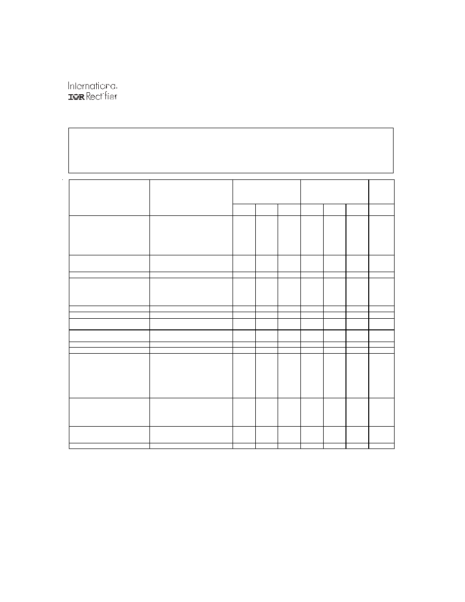
ATR28XXD Series
T
CASE
= -55∞C to +125∞C, V
IN
= +28V
±
5% unless otherwise specified
ABSOLUTE MAXIMUM RATINGS
Input Voltage -0.5V to 50VDC
Power Output Internally limited, 36W typical
Soldering 300
∞
C for 10 seconds
Temperature Range
1
Recommended Operating -55
∞
C to +125
∞
C
Maximum Operating -55
∞
C to +135
∞
C
Storage -65
∞
C to +135
∞
C
ATR2812D/HB
ATR2815D/HB
PARAMETER
Condition
-55
∞
C
TC
+125
∞
C, V
IN
= 28 V
DC
±
5%, CL=0, unless otherwise
specified
Min Typ Max Min Typ Max Units
STATIC
CHARACTERISTICS
OUTPUT
V
IN
= 16 to 40 V
DC
Voltage
I
OUT
= 0 to Full Load
±
11.76
±
12.00
±
12.24
±
14.70
±
15.00
±
15.30
V
DC
Current
5
0.0
±
1.25
0.0
±
1.0
A
DC
Ripple
Full Load, 20KHz to 2MHz
40
85
40
85
mV p-p
Accuracy
T
CASE
= 25
∞
C, Full Load
±
11.88
±
12.00
±
12.12
±
14.85
±
15.00
±
15.15
V
DC
Power
1
30 30 W
REGULATION
Line
4
Load
4
V
IN
= 16 to 40 V
DC
I
OUT
= 0 to Full Load
75
120
75
150
mV
mV
CROSS REGULATION
6
V
IN
= 16, 28, and 40 V
DC
±
5
±
5
%
INPUT
Voltage Range
Current
Ripple Current
No Load, pin 2 = open
Inhibited, pin 2 tied to pin 10
Full Load
16.0
28.0
25
40.0
75
18
50
16.0
28.0
18
25
40.0
75
18
50
V
DC
mA
DC
mA
DC
mA p-p
EFFICIENCY
Full Load T
C
= +25
∞
C
80 82 79 82
%
ISOLATION
Input to output @500 V
DC
100 100 M
CAPACITIVE LOAD
No effect on performance
T
C
= +25
∞
C (total for both outputs)
100
100
µ
F
Load Fault Power Dissipation
Short Circuit
Overload, T
C
= +25
∞
C
9
14
9
14
W
W
Switching Frequency
I
OUT
= Full Load
500
600
500
600
KHz
SYNC Frequency Range
7
500 700
500 700
KHz
DYNAMIC
CHARACTERISTICS
Step Load Changes
Output
4
Transient
Recovery
2
50% Load to
100% Load
No Load to 50% Load
50% Load to 100% Load
No Load to 50% Load
50% Load to No Load
±
100
±
250
25
500
3
±
450
±
760
70
1500
5
±
100
±
250
25
500
3
±
450
±
750
70
1500
5
mVpk
mVpk
µ
s
µ
s
ms
Step Line Changes
Output
Transient
Recovery
2
Input step 16 to 40
VDC
Input step 40 to 16 V
DC
Input step 16 to 40 V
DC
Input step 40 to 16 V
DC
±
180
-600
5
5
1200
-1500
10
10
±
180
-600
5
5
1500
-1500
10
10
mVpk
mVpk
ms
ms
TURN-ON
Overshoot
Delay
3
V
IN
= 16 to 40 V
DC
I
OUT
= O to Full Load
0
14
600
25
0
14
600
25
mVpk
ms
Load Fault Recovery
V
IN
= 16 to 40 V
DC
14
25 14
25 ms
Notes to Specifications
1. Above +125
∞
C case temperature, derate output power linearly to 0 at +135
∞
C case.
2. Recovery time is measured from the initiation of the input transient to where V
OUT
has returned to within
±
1% of V
OUT
at 50% load.
3. Turn-on delay time measurement is for either an application of power at the input or a signal at the inhibit pin.
4. Load current split equally between +V
OUT
and ≠V
OUT
.
5. Up to 90% of Full Power is available from either output provided. The total power output does not exceed 30 watts.
6. 3W load on output under test, 3W to 27W on other output.
7. Sync. Input signal: V
IL
= -0.5V Min, V
IN
= 2.5V Min, 10% to 90% duty cycle
0.8V Max, 11.5V Max
Specifications
www.irf.com
5
ATR28XXD Series
T
CASE
= -55∞C to +125∞C, V
IN
= +28V
±
5% unless otherwise specified
ABSOLUTE MAXIMUM RATINGS
Input Voltage -0.5V to 50VDC
Power Output Internally limited, 36W typical
Soldering 300
∞
C for 10 seconds
Temperature Range
1
Recommended Operating -55
∞
C to +125
∞
C
Maximum Operating -55
∞
C to +135
∞
C
Storage -65
∞
C to +135
∞
C
Specifications
ATR2812D/CH
ATR2815D/CH
PARAMETER
Condition
-55
∞
C
TC
+125
∞
C, V
IN
= 28 V
DC
±
5%, CL=0, unless otherwise
specified
Min Typ Max Min Typ Max Units
STATIC
CHARACTERISTICS
OUTPUT
V
IN
= 16 to 40 V
DC
Voltage
I
OUT
= 0 to Full Load
±
11.76
±
12.00
±
12.24
±
14.70
±
15.00
±
15.30
V
DC
Current
5
0.0
±
1.25
0.0
±
1.0
A
DC
Ripple
Full Load, 20KHz to 2MHz
40
85
40
85
mV p-p
Accuracy
T
CASE
= 25
∞
C, Full Load
±
11.88
±
12.00
±
12.12
±
14.85
±
15.00
±
15.15
V
DC
Power
1
30 30 W
REGULATION
Line
4
Load
4
V
IN
= 16 to 40 V
DC
I
OUT
= 0 to Full Load
75
120
75
150
mV
mV
CROSS REGULATION
6
V
IN
= 16, 28, and 40 V
DC
±
5
±
5
%
INPUT
Voltage Range
Current
Ripple Current
No Load, pin 2 = open
Inhibited, pin 2 tied to pin 10
Full Load
16.0
28.0
25
40.0
75
18
50
16.0
28.0
18
25
40.0
75
18
50
V
DC
mA
DC
mA
DC
mA p-p
EFFICIENCY
Full Load T
C
= +25
∞
C
80
82 79
82 %
ISOLATION
Input to output @500 V
DC
100 100 M
CAPACITIVE LOAD
No effect on performance
T
C
= +25
∞
C (total for both outputs)
100
100
µ
F
Load Fault Power Dissipation
Short Circuit
Overload, T
C
= +25
∞
C
9
14
9
14
W
W
Switching Frequency
I
OUT
= Full Load
500
600
500
600
KHz
SYNC Frequency Range
7
500 700
500 700
KHz
DYNAMIC
CHARACTERISTICS
Step
Load
Changes
Output
4
Transient
Recovery
2
50% Load to
100% Load
No Load to 50% Load
50% Load to 100% Load
No Load to 50% Load
50% Load to No Load
±
100
±
250
25
500
3
±
450
±
760
70
1500
5
±
100
±
250
25
500
3
±
450
±
750
70
1500
5
mVpk
mVpk
µ
s
µ
s
ms
Step Line Changes
Output
Transient
Recovery
2
Input step 16 to 40
VDC
Input step 40 to 16 V
DC
Input step 16 to 40 V
DC
Input step 40 to 16 V
DC
±
180
-600
5
5
1200
-1500
10
10
±
180
-600
5
5
1500
-1500
10
10
mVpk
mVpk
ms
ms
TURN-ON
Overshoot
Delay
3
V
IN
= 16 to 40 V
DC
I
OUT
= 0 to Full Load
0
14
600
25
0
14
600
25
mVpk
ms
Load Fault Recovery
V
IN
= 16 to 40 V
DC
14
25 14
25 ms
Notes to Specifications
1. Above +125
∞
C case temperature, derate output power linearly to 0 at +135
∞
C case.
2. Recovery time is measured from the initiation of the input transient to where V
OUT
has returned to within
±
1% of V
OUT
at 50% load.
3. Turn-on delay time measurement is for either an application of power at the input or a signal at the inhibit pin.
4. Load current split equally between +V
OUT
and ≠V
OUT
.
5. Up to 90% of Full Power is available from either output provided. The total power output does not exceed 30 watts.
6. 3W load on output under test, 3W to 27W on other output.
7. Sync. Input signal: V
IL
= -0.5V Min, V
IN
= 2.5V Min, 10% to 90% duty cycle
0.8V Max, 11.5V Max