
Parameter
Max.
Units
I
D
@ T
C
= 25∞C
Continuous Drain Current, V
GS
@ 10V
38
I
D
@ T
C
= 100∞C
Continuous Drain Current, V
GS
@ 10V
24
A
I
DM
Pulsed Drain Current
150
P
D
@T
C
= 25∞C
Power Dissipation
500
W
Linear Derating Factor
4.0
W/∞C
V
GS
Gate-to-Source Voltage
± 20
V
E
AS
Single Pulse Avalanche Energy
580
mJ
I
AR
Avalanche Current
38
A
E
AR
Repetitive Avalanche Energy
50
mJ
dv/dt
Peak Diode Recovery dv/dt
16
V/ns
T
J
Operating Junction and
-55 to + 150
∞C
T
STG
Storage Temperature Range
V
ISO
Insulation Withstand Voltage (AC-RMS)
2.5
kV
Mounting torque, M4 srew
(1.3N∑M)
FA38SA50LC
HEXFET
Æ
Power MOSFET
S
D
G
V
DSS
= 500V
R
DS(on)
= 0.13
I
D
= 38A
Third Generation HEXFETs from International Rectifier
provide the designer with the best combination of fast
switching, ruggedized device design, low on-resistance
and cost-effectiveness.
The SOT-227 package is universally preferred for all
commercial-industrial applications at power dissipation
levels to approximately 500 watts. The low thermal
resistance of the SOT-227 contribute to its wide acceptance
throughout the industry.
2/2/99
Description
l
Fully Isolated Package
l
Easy to Use and Parallel
l
Low On-Resistance
l
Dynamic dv/dt Rating
l
Fully Avalanche Rated
l
Simple Drive Requirements
l
Low Drain to Case Capacitance
l
Low Internal Inductance
S O T -2 2 7
Absolute Maximum Ratings
Parameter
Typ.
Max.
Units
R
JC
Junction-to-Case
≠≠≠
0.25
R
CS
Case-to-Sink, Flat, Greased Surface
0.05
≠≠≠
∞C/W
Thermal Resistance
www.irf.com
1
PD - 91615B

FA38SA50LC
2
www.irf.com
Repetitive rating; pulse width limited by
max. junction temperature. ( See fig. 11 )
I
SD
38A, di/dt
410A/µs, V
DD
V
(BR)DSS
,
T
J
150∞C
Notes:
Starting T
J
= 25∞C, L = 0.80mH
R
G
= 25
, I
AS
= 38A. (See Figure 12)
Pulse width
300µs; duty cycle
2%.
Parameter
Min. Typ. Max. Units
Conditions
I
S
Continuous Source Current
MOSFET symbol
(Body Diode)
≠≠≠
≠≠≠
showing the
I
SM
Pulsed Source Current
integral reverse
(Body Diode)
≠≠≠
≠≠≠
p-n junction diode.
V
SD
Diode Forward Voltage
≠≠≠
≠≠≠
1.3
V
T
J
= 25∞C, I
S
= 38A, V
GS
= 0V
t
rr
Reverse Recovery Time
≠≠≠
830 1300
ns
T
J
= 25∞C, I
F
= 38A
Q
rr
Reverse RecoveryCharge
≠≠≠
15
22
µC
di/dt = 100A/µs
t
on
Forward Turn-On Time
Intrinsic turn-on time is negligible (turn-on is dominated by L
S
+L
D
)
Source-Drain Ratings and Characteristics
A
38
150
Parameter
Min. Typ. Max. Units
Conditions
V
(BR)DSS
Drain-to-Source Breakdown Voltage
500
≠≠≠
≠≠≠
V
V
GS
= 0V, I
D
= 1.0mA
V
(BR)DSS
/
T
J
Breakdown Voltage Temp. Coefficient
≠≠≠
0.66
≠≠≠
V/∞C
Reference to 25∞C, I
D
= 1mA
R
DS(on)
Static Drain-to-Source On-Resistance
≠≠≠
≠≠≠
0.13
V
GS
= 10V, I
D
= 23A
V
GS(th)
Gate Threshold Voltage
2.0
≠≠≠
4.0
V
V
DS
= V
GS
, I
D
= 250µA
g
fs
Forward Transconductance
22
≠≠≠
≠≠≠
S
V
DS
= 25V, I
D
= 23A
≠≠≠
≠≠≠
50
µA
V
DS
= 500V, V
GS
= 0V
≠≠≠
≠≠≠
500
V
DS
= 400V, V
GS
= 0V, T
J
= 125∞C
Gate-to-Source Forward Leakage
≠≠≠
≠≠≠
200
V
GS
= 20V
Gate-to-Source Reverse Leakage
≠≠≠
≠≠≠
-200
nA
V
GS
= -20V
Q
g
Total Gate Charge
≠≠≠
280
420
I
D
= 38A
Q
gs
Gate-to-Source Charge
≠≠≠
37
55
nC
V
DS
= 400V
Q
gd
Gate-to-Drain ("Miller") Charge
≠≠≠
150
220
V
GS
= 10V, See Fig. 6 and 13
t
d(on)
Turn-On Delay Time
≠≠≠
42
≠≠≠
V
DD
= 250V
t
r
Rise Time
≠≠≠
340
≠≠≠
I
D
= 38A
t
d(off)
Turn-Off Delay Time
≠≠≠
200
≠≠≠
R
G
= 10
(Internal)
t
f
Fall Time
≠≠≠
330
≠≠≠
R
D
= 8
,
See Fig. 10
L
s
Internal Source Inductance
≠≠≠
5.0
≠≠≠
nH
Between lead,
and center of die contact
C
iss
Input Capacitance
≠≠≠
6900 ≠≠≠
V
GS
= 0V
C
oss
Output Capacitance
≠≠≠
1600 ≠≠≠
pF
V
DS
= 25V
C
rss
Reverse Transfer Capacitance
≠≠≠
580
≠≠≠
= 1.0MHz, See Fig. 5
Electrical Characteristics @ T
J
= 25∞C (unless otherwise specified)
I
GSS
ns
I
DSS
Drain-to-Source Leakage Current
FA38SA50LC
www.irf.com
3
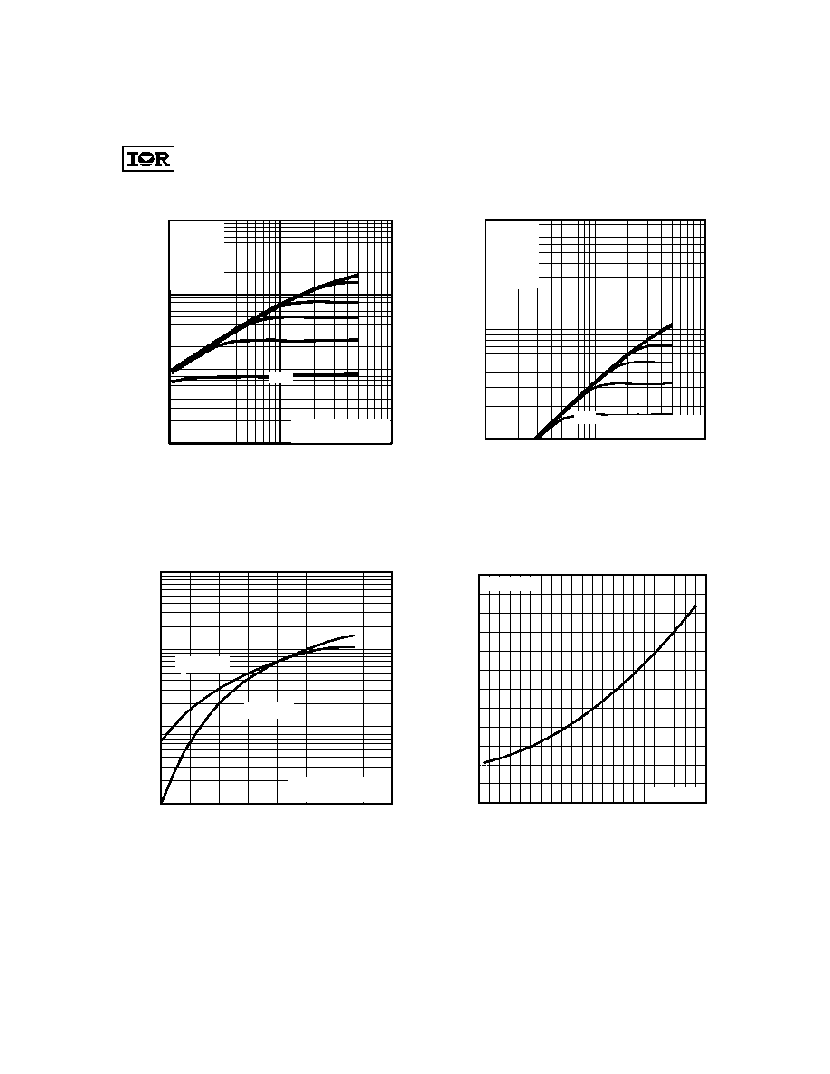
Fig 3. Typical Transfer Characteristics
Fig 4. Normalized On-Resistance
Vs. Temperature
Fig 1. Typical Output Characteristics
Fig 2. Typical Output Characteristics
1
1 0
1 0 0
1 0 0 0
1
1 0
1 0 0
V , D rain-to-So urce V oltag e (V )
20µ s P U LS E W ID TH
T = 25∞C
C
A
4.5V
VGS
T O P 1 5V
10V
8.0V
7.0V
6.0V
5.5V
5.0V
B OT T O M 4.5V
D S
1
10
100
1000
4
5
6
7
8
V = 50V
20µs PULSE WIDTH
DS
V , Gate-to-Source Voltage (V)
I , Drain-to-Source Current (A)
GS
D
T = 25 C
J
∞
T = 150 C
J
∞
-60 -40 -20
0
20
40
60
80 100 120 140 160
0.0
0.5
1.0
1.5
2.0
2.5
3.0
T , Junction Temperature ( C)
R , Drain-to-Source On Resistance
(Normalized)
J
DS(on)
∞
V
=
I =
GS
D
10V
38A
I
D
, Drain-to-Source Current (A)
10
100
1000
1
10
100
20µs PULSE WIDTH
T = 150 C
J
∞
TOP
BOTTOM
VGS
15V
10V
8.0V
7.0V
6.0V
5.5V
5.0V
4.5V
V , Drain-to-Source Voltage (V)
I , Drain-to-Source Current (A)
DS
D
4.5V
FA38SA50LC
4
www.irf.com
Fig 8. Maximum Safe Operating Area
Fig 6. Typical Gate Charge Vs.
Gate-to-Source Voltage
Fig 5. Typical Capacitance Vs.
Drain-to-Source Voltage
Fig 7. Typical Source-Drain Diode
Forward Voltage
0
80
160
240
320
400
0
4
8
12
16
20
Q , Total Gate Charge (nC)
V , Gate-to-Source Voltage (V)
G
GS
FOR TEST CIRCUIT
SEE FIGURE
I =
D
13
38A
V
= 100V
DS
V
= 250V
DS
V
= 400V
DS
1
10
100
1000
1
10
100
1000
10000
OPERATION IN THIS AREA LIMITED
BY R
DS(on)
Single Pulse
T
T
= 150 C
= 25 C
∞
∞
J
C
V , Drain-to-Source Voltage (V)
I , Drain Current (A)
I , Drain Current (A)
DS
D
10us
100us
1ms
10ms
0.1
1
10
100
1000
0.2
0.4
0.6
0.8
1.0
1.2
1.4
1.6
V ,Source-to-Drain Voltage (V)
I , Reverse Drain Current (A)
SD
SD
V = 0 V
GS
T = 25 C
J
∞
T = 150 C
J
∞
1
10
100
0
2000
4000
6000
8000
10000
12000
14000
16000
V , Drain-to-Source Voltage (V)
C, Capacitance (pF)
DS
V
C
C
C
=
=
=
=
0V,
C
C
C
f = 1MHz
+ C
+ C
C SHORTED
GS
iss
gs
gd ,
ds
rss
gd
oss
ds
gd
Ciss
Coss
Crss

FA38SA50LC
www.irf.com
5
Q
G
Q
GS
Q
GD
V
G
Charge
+
-
V
DS
10V
Pulse Width
1
µs
Duty Factor
0.1 %
R
D
V
GS
V
DD
R
G
D.U.T.
D.U.T.
V
DS
I
D
I
G
3mA
V
GS
.3
µ
F
50K
.2
µ
F
12V
Current Regulator
Same Type as D.U.T.
Current Sampling Resistors
+
-
V
DS
90%
10%
V
GS
t
d(on)
t
r
t
d(off)
t
f
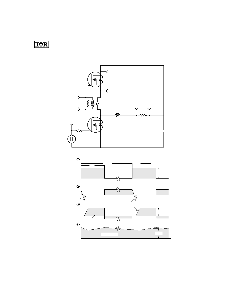
Fig 10b. Switching Time Waveforms
Fig 10a. Switching Time Test Circuit
Fig 9a. Basic Gate Charge Waveform
Fig 9b. Gate Charge Test Circuit
Fig 11. Maximum Effective Transient Thermal Impedance, Junction-to-Case
10V
0.001
0.01
0.1
1
0.00001
0.0001
0.001
0.01
0.1
1
Notes:
1. Duty factor D = t / t
2. Peak T = P
x Z
+ T
1
2
J
DM
thJC
C
P
t
t
DM
1
2
t , Rectangular Pulse Duration (sec)
Thermal Response
(Z )
1
thJC
0.01
0.02
0.05
0.10
0.20
0.50
SINGLE PULSE
(THERMAL RESPONSE)

FA38SA50LC
6
www.irf.com
Fig 12c. Maximum Avalanche Energy
Vs. Drain Current
Fig 12b. Unclamped Inductive Waveforms
Fig 12a. Unclamped Inductive Test Circuit
tp
V
(B R )D SS
I
A S
R G
I
A S
0 .0 1
tp
D .U .T
L
V D S
+
-
VD D
D R IV E R
A
1 5 V
20 V
25
50
75
100
125
150
0
200
400
600
800
1000
1200
Starting T , Junction Temperature ( C)
E , Single Pulse Avalanche Energy (mJ)
J
AS
∞
ID
TOP
BOTTOM
17A
24A
38A
FA38SA50LC
www.irf.com
7
P.W.
Period
di/dt
Diode Recovery
dv/dt
Ripple
5%
Body Diode
Forward Drop
Re-Applied
Voltage
Reverse
Recovery
Current
Body Diode Forward
Current
V
GS
=10V
V
DD
I
SD
Driver Gate Drive
D.U.T. I
SD
Waveform
D.U.T. V
DS
Waveform
Inductor Curent
D =
P.W.
Period
+
-
+
+
+
-
-
-
*
V
GS
= 5V for Logic Level Devices
Peak Diode Recovery dv/dt Test Circuit
R
G
V
DD
∑
dv/dt controlled by R
G
∑
Driver same type as D.U.T.
∑
I
SD
controlled by Duty Factor "D"
∑
D.U.T. - Device Under Test
D.U.T
Circuit Layout Considerations
∑
Low Stray Inductance
∑
Ground Plane
∑
Low Leakage Inductance
Current Transformer
*
Fig 13. For N-Channel HEXFETS

FA38SA50LC
8
www.irf.com
Tube
SOT-227 Package Details
4 .4 0 (.17 3 )
4 .2 0 (.16 5 )
1 2.50 ( .4 92 )
7 .50 ( .29 5 )
2 .1 0 ( .0 82 )
1 .9 0 ( .0 75 )
3 0 .2 0 ( 1 .1 89 )
2 9 .8 0 ( 1 .1 73 )
8.10 ( .3 19 )
7.70 ( .3 03 )
4 X
1 5.00 ( .5 90 )
R F U L L
2 .10 ( .08 2 )
1 .90 ( .07 5 )
0.1 2 ( .00 5 )
-C -
0 .25 ( .01 0 ) M C A M B M
2 5 .7 0 ( 1.0 12 )
2 5 .2 0 ( .9 9 2 )
-B -
6.2 5 ( .24 6 )
C H A M F E R
2 .0 0 ( .0 7 9 ) X 45 7
-A -
3 8 .3 0 ( 1.5 08 )
3 7 .8 0 ( 1.4 88 )
12 .3 0 ( .4 84 )
11 .8 0 ( .4 64 )
4
1
3
2
L E A D A S S IG M E N T S
IG B T
E
C
G
E
S
D
G
S
H E X F E T
A 1
K 2
K 1
A 2
3
2
4
1
3
2
4
1
H E X F R E D
QUANTITY PER TU BE IS 1 0
M4 SREW AND W ASHE R IN CLUDED
WORLD HEADQUARTERS: 233 Kansas St., El Segundo, California 90245, Tel: (310) 322 3331
IR GREAT BRITAIN: Hurst Green, Oxted, Surrey RH8 9BB, UK Tel: ++ 44 1883 732020
IR CANADA: 15 Lincoln Court, Brampton, Ontario L6T3Z2, Tel: (905) 453 2200
IR GERMANY: Saalburgstrasse 157, 61350 Bad Homburg Tel: ++ 49 6172 96590
IR ITALY: Via Liguria 49, 10071 Borgaro, Torino Tel: ++ 39 11 451 0111
IR FAR EAST: K&H Bldg., 2F, 30-4 Nishi-Ikebukuro 3-Chome, Toshima-Ku, Tokyo Japan 171 Tel: 81 3 3983 0086
IR SOUTHEAST ASIA: 1 Kim Seng Promenade, Great World City West Tower, 13-11, Singapore 237994 Tel: ++ 65 838 4630
IR TAIWAN:16 Fl. Suite D. 207, Sec. 2, Tun Haw South Road, Taipei, 10673, Taiwan Tel: 886-2-2377-9936
http://www.irf.com/ Data and specifications subject to change without notice. 2/99