 | –≠–ª–µ–∫—Ç—Ä–æ–Ω–Ω—ã–π –∫–æ–º–ø–æ–Ω–µ–Ω—Ç: FB180SA10 | –°–∫–∞—á–∞—Ç—å:  PDF PDF  ZIP ZIP |
Parameter
Max.
Units
I
D
@ T
C
= 25∞C
Continuous Drain Current, V
GS
@ 10V
180
I
D
@ T
C
= 100∞C
Continuous Drain Current, V
GS
@ 10V
120
A
I
DM
Pulsed Drain Current
720
P
D
@T
C
= 25∞C
Power Dissipation
480
W
Linear Derating Factor
2.7
W/∞C
V
GS
Gate-to-Source Voltage
± 20
V
E
AS
Single Pulse Avalanche Energy
700
mJ
I
AR
Avalanche Current
180
A
E
AR
Repetitive Avalanche Energy
48
mJ
dv/dt
Peak Diode Recovery dv/dt
5.7
V/ns
T
J
Operating Junction and
-55 to + 150
∞C
T
STG
Storage Temperature Range
V
ISO
Insulation Withstand Voltage (AC-RMS)
2.5
kV
Mounting torque, M4 srew
1.3
N∑m
FB180SA10
HEXFET
Æ
Power MOSFET
PD- 91651C
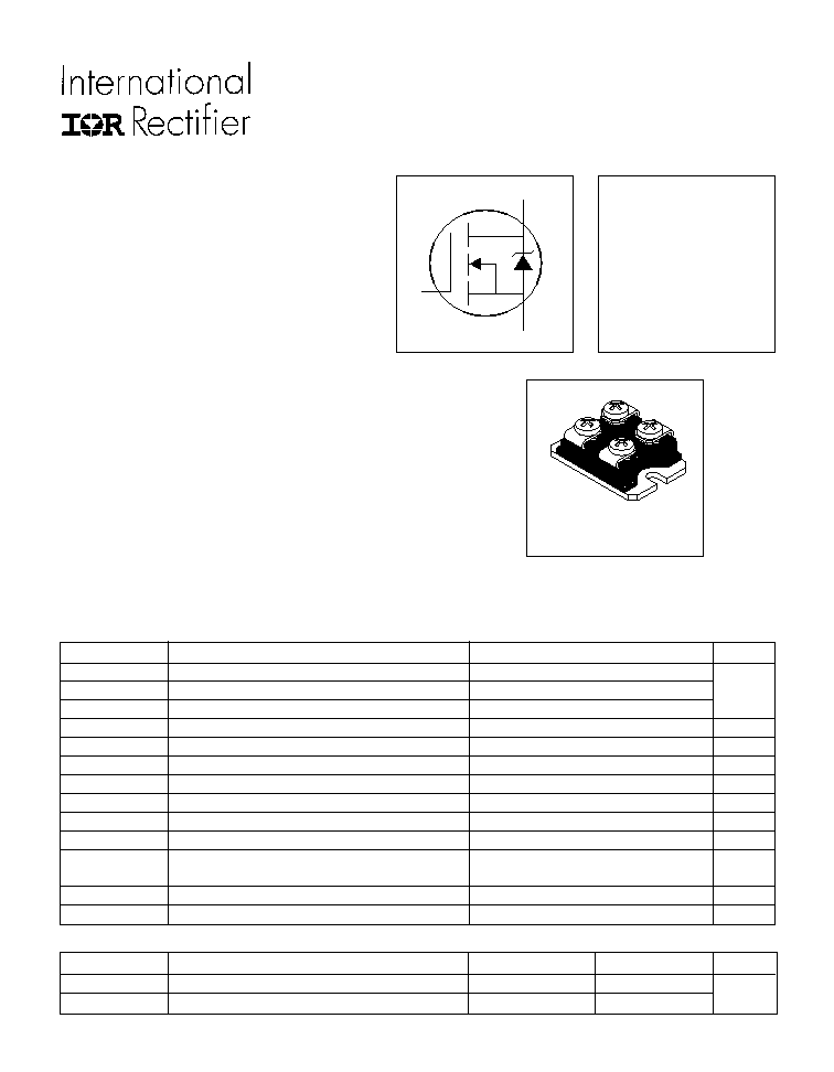
S
D
G
V
DSS
= 100V
R
DS(on)
= 0.0065
W
I
D
= 180A
Fifth Generation, high current density HEXFETS are
paralled into a compact, high power module providing
the best combination of switching, ruggedized design,
very low ON resistance and cost effectiveness.
The isolated SOT-227 package is preferred for all
c o m m e r c i a l - i n d u s t r i a l a p p l i c a t i o n s a t p o w e r
dissipation levels to approximately 500 watts. The low
thermal resistance and easy connection to the SOT-
227 package contribute to its universal acceptance
throughout the industry.
2/1/99
Description
l
Fully Isolated Package
l
Easy to Use and Parallel
l
Very Low On-Resistance
l
Dynamic dv/dt Rating
l
Fully Avalanche Rated
l
Simple Drive Requirements
l
Low Drain to Case Capacitance
l
Low Internal Inductance
S O T -22 7
Absolute Maximum Ratings
Parameter
Typ.
Max.
Units
R
q
JC
Junction-to-Case
≠≠≠
0.26
R
q
CS
Case-to-Sink, Flat, Greased Surface
0.05
≠≠≠
∞C/W
Thermal Resistance
1
www.irf.com
FB180SA10
2
www.irf.com
Repetitive rating; pulse width limited by
max. junction temperature. ( See fig. 11 )
I
SD
£
180A, di/dt
£
83A/µs, V
DD
£
V
(BR)DSS
,
T
J
£
150∞C
Notes:
Starting T
J
= 25∞C, L =43µH
R
G
= 25
W
, I
AS
= 180A. (See Figure 12)
Pulse width
£
300µs; duty cycle
£
2%.
Parameter
Min. Typ. Max. Units
Conditions
I
S
Continuous Source Current
MOSFET symbol
(Body Diode)
≠≠≠
≠≠≠
showing the
I
SM
Pulsed Source Current
integral reverse
(Body Diode)
≠≠≠
≠≠≠
p-n junction diode.
V
SD
Diode Forward Voltage
≠≠≠
≠≠≠
1.3
V
T
J
= 25∞C, I
S
= 180A, V
GS
= 0V
t
rr
Reverse Recovery Time
≠≠≠ 300 450 ns
T
J
= 25∞C, I
F
= 180A
Q
rr
Reverse Recovery Charge
≠≠≠
2.6
3.9
µC
di/dt = 100A/µs
t
on
Forward Turn-On Time
Intrinsic turn-on time is negligible (turn-on is dominated by L
S
+L
D
)
Source-Drain Ratings and Characteristics
A
180
720
Parameter
Min. Typ. Max. Units
Conditions
V
(BR)DSS
Drain-to-Source Breakdown Voltage
100
≠≠≠
≠≠≠
V
V
GS
= 0V, I
D
= 250µA
D
V
(BR)DSS
/
D
T
J
Breakdown Voltage Temp. Coefficient
≠≠≠
0.093 ≠≠≠
V/∞C
Reference to 25∞C, I
D
= 1mA
R
DS(on)
Static Drain-to-Source On-Resistance
≠≠≠
≠≠≠ 0.0065
W
V
GS
= 10V, I
D
= 108A
V
GS(th)
Gate Threshold Voltage
2.0
≠≠≠
4.0
V
V
DS
= V
GS
, I
D
= 250µA
g
fs
Forward Transconductance
93
≠≠≠
≠≠≠
S
V
DS
= 25V, I
D
= 108A
≠≠≠
≠≠≠
50
µA
V
DS
= 100V, V
GS
= 0V
≠≠≠
≠≠≠
500
V
DS
= 80V, V
GS
= 0V, T
J
= 125∞C
Gate-to-Source Forward Leakage
≠≠≠
≠≠≠
200
V
GS
= 20V
Gate-to-Source Reverse Leakage
≠≠≠
≠≠≠
-200
nA
V
GS
= -20V
Q
g
Total Gate Charge
≠≠≠
250
380
I
D
= 180A
Q
gs
Gate-to-Source Charge
≠≠≠
40
60
nC
V
DS
= 80V
Q
gd
Gate-to-Drain ("Miller") Charge
≠≠≠
110
165
V
GS
= 10.0V, See Fig. 6 and 13
t
d(on)
Turn-On Delay Time
≠≠≠
45
≠≠≠
V
DD
= 50V
t
r
Rise Time
≠≠≠
351
≠≠≠
I
D
= 180A
t
d(off)
Turn-Off Delay Time
≠≠≠
181
≠≠≠
R
G
= 2.0
W
(Internal)
t
f
Fall Time
≠≠≠
335
≠≠≠
R
D
= 0.27
W,
See Fig. 10
L
s
Internal Source Inductance
≠≠≠
5.0
≠≠≠
nH
Between lead,
and center of die contact
C
iss
Input Capacitance
≠≠≠ 10700 ≠≠≠
V
GS
= 0V
C
oss
Output Capacitance
≠≠≠
2800 ≠≠≠
pF
V
DS
= 25V
C
rss
Reverse Transfer Capacitance
≠≠≠
1300 ≠≠≠
= 1.0MHz, See Fig. 5
Electrical Characteristics @ T
J
= 25∞C (unless otherwise specified)
I
GSS
ns
I
DSS
Drain-to-Source Leakage Current
FB180SA10
www.irf.com
3
Fig 4. Normalized On-Resistance
Vs. Temperature
Fig 2. Typical Output Characteristics
Fig 1. Typical Output Characteristics
Fig 3. Typical Transfer Characteristics
1
10
100
1000
0.1
1
10
100
20µs PULSE WIDTH
T = 25 C
J
∞
TOP
BOTTOM
VGS
15V
10V
8.0V
7.0V
6.0V
5.5V
5.0V
4.5V
V , Drain-to-Source Voltage (V)
I , Drain-to-Source Current (A)
DS
D
4.5V
1
10
100
1000
0.1
1
10
100
20µs PULSE WIDTH
T = 150 C
J
∞
TOP
BOTTOM
VGS
15V
10V
8.0V
7.0V
6.0V
5.5V
5.0V
4.5V
V , Drain-to-Source Voltage (V)
I , Drain-to-Source Current (A)
DS
D
4.5V
1
10
100
1000
4
5
6
7
8
9
10
V = 25V
20µs PULSE WIDTH
DS
V , Gate-to-Source Voltage (V)
I , Drain-to-Source Current (A)
GS
D
T = 25 C
J
∞
T = 150 C
J
∞
-60 -40 -20
0
20
40
60
80 100 120 140 160
0.0
0.5
1.0
1.5
2.0
2.5
T , Junction Temperature( C)
R , Drain-to-Source On Resistance
(Normalized)
J
DS(on)
∞
V
=
I =
GS
D
10V
180A

FB180SA10
4
www.irf.com
Fig 8. Maximum Safe Operating Area
Fig 6. Typical Gate Charge Vs.
Gate-to-Source Voltage
Fig 5. Typical Capacitance Vs.
Drain-to-Source Voltage
Fig 7. Typical Source-Drain Diode
Forward Voltage
0.1
1
10
100
1000
0.2
0.6
1.0
1.4
1.8
V ,Source-to-Drain Voltage (V)
I , Reverse Drain Current (A)
SD
SD
V = 0 V
GS
T = 150 C
J
∞
T = 25 C
J
∞
1
10
100
0
5000
10000
15000
20000
V , Drain-to-Source Voltage (V)
C, Capacitance (pF)
DS
V
C
C
C
=
=
=
=
0V,
C
C
C
f = 1MHz
+ C
+ C
C SHORTED
GS
iss
gs
gd ,
ds
rss
gd
oss
ds
gd
C
iss
C
oss
C
rss
0
50
100
150
200
250
300
350
400
0
5
10
15
20
Q , Total Gate Charge (nC)
V , Gate-to-Source Voltage (V)
G
GS
FOR TEST CIRCUIT
SEE FIGURE
I =
D
13
180 A
V
= 20V
DS
V
= 50V
DS
V
= 80V
DS
1
10
100
1000
10000
1
10
100
1000
OPERATION IN THIS AREA LIMITED
BY R
DS(on)
Single Pulse
T
T
= 150 C
= 25 C
∞
∞
J
C
V , Drain-to-Source Voltage (V)
I , Drain Current (A)
I , Drain Current (A)
DS
D
10us
100us
1ms
10ms
FB180SA10
www.irf.com
5
Fig 10a. Switching Time Test Circuit
V
DS
90%
10%
V
GS
t
d(on)
t
r
t
d(off)
t
f
Fig 10b. Switching Time Waveforms
V
DS
Pulse Width
£ 1
µs
Duty Factor
£ 0.1 %
R
D
V
GS
R
G
D.U.T.
10V
+
-
V
DD
Fig 11. Maximum Effective Transient Thermal Impedance, Junction-to-Case
Fig 9. Maximum Drain Current Vs.
Case Temperature
25
50
75
100
125
150
0
25
50
75
100
125
150
175
200
T , Case Temperature ( C)
I , Drain Current (A)
∞
C
D
0.001
0.01
0.1
1
0.00001
0.0001
0.001
0.01
0.1
Notes:
1. Duty factor D = t / t
2. Peak T = P
x Z
+ T
1
2
J
DM
thJC
C
P
t
t
DM
1
2
t , Rectangular Pulse Duration (sec)
Thermal Response
(Z )
1
thJC
0.01
0.02
0.05
0.10
0.20
D = 0.50
SINGLE PULSE
(THERMAL RESPONSE)