www.irf.com
1
HEXFET
Æ
Power MOSFET
Benefits
Applications
!
Low Gate Charge Qg results in Simple
Drive Requirement
!
Improved Gate, Avalanche and Dynamic
dv/dt Ruggedness
!
Fully Characterized Capacitance and
Avalanche Voltage and Current
!
Low R
DS(on)
!
Fully Insulated Package
Parameter
Max.
Units
I
D
@ T
C
= 25∞C
Continuous Drain Current, V
GS
@ 10V
40
I
D
@ T
C
= 100∞C
Continuous Drain Current, V
GS
@ 10V
26
A
I
DM
Pulsed Drain Current
"
160
P
D
@T
C
= 25∞C
Power Dissipation
430
W
Linear Derating Factor
3.45
W/∞C
V
GS
Gate-to-Source Voltage
± 30
V
dv/dt
Peak Diode Recovery dv/dt
#
9.0
V/ns
T
J
Operating Junction and
-55 to + 150
∞C
T
STG
Storage Temperature Range
Absolute Maximum Ratings
Avalanche Characteristics
Symbol
Parameter
Typ.
Max.
Units
E
AS
Single Pulse Avalanche Energy
$
≠
1240
mJ
I
AR
Avalanche Current
"
≠
40
A
E
AR
Repetitive Avalanche Energy
"
≠
43
mJ
Symbol
Parameter
Typ.
Max.
Units
R
JC
Junction-to-Case
≠
0.29
∞C/W
R
CS
Case-to-Sink, Flat, Greased Surface
0.05
≠
Thermal Resistance
V
DSS
R
DS(on)
typ.
I
D
500V
0.084
40A
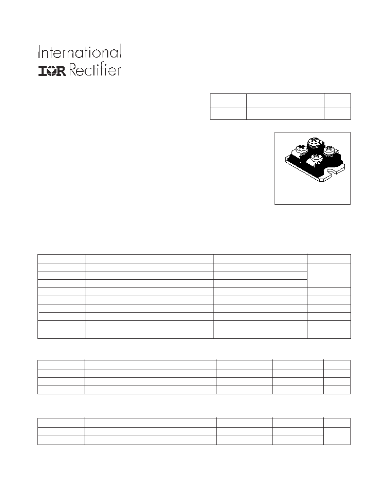
SOT-227
FC40SA50FK
I27139- 01/03
!
Switch Mode Power Supply (SMPS)
!
Uninterruptible Power Supply
!
High Speed Power Switching
!
Hard Switched and High Frequency Circuits
2
www.irf.com
I27139- 01/03
FC40SA50FK
Symbol
Parameter
Min. Typ. Max. Units
Conditions
g
fs
Forward Transconductance
23
≠
≠
S
V
DS
= 50V, I
D
= 28A
Q
g
Total Gate Charge
≠
≠
270
I
D
= 40A
Q
gs
Gate-to-Source Charge
≠
≠
84
nC
V
DS
= 400V
Q
gd
Gate-to-Drain ("Miller") Charge
≠
≠
130
V
GS
= 10V, See Fig. 6 and 13
%
t
d(on)
Turn-On Delay Time
≠
25
≠
V
DD
= 250V
t
r
Rise Time
≠
140
≠
I
D
= 40A
t
d(off)
Turn-Off Delay Time
≠
55
≠
R
G
= 1.0
t
f
Fall Time
≠
74
≠
V
GS
= 10V,See Fig. 10
%
C
iss
Input Capacitance
≠
8310
≠
V
GS
= 0V
C
oss
Output Capacitance
≠
960
≠
V
DS
= 25V
C
rss
Reverse Transfer Capacitance
≠
120
≠
pF
= 1.0MHz, See Fig. 5
C
oss
Output Capacitance
≠
10170
≠
V
GS
= 0V, V
DS
= 1.0V, = 1.0MHz
C
oss
Output Capacitance
≠
240
≠
V
GS
= 0V, V
DS
= 480V, = 1.0MHz
C
oss
eff.
Effective Output Capacitance
≠
440
≠
V
GS
= 0V, V
DS
= 0V to 480V
'
Dynamic @ T
J
= 25∞C (unless otherwise specified)
ns
Symbol
Parameter
Min. Typ. Max. Units
Conditions
V
(BR)DSS
Drain-to-Source Breakdown Voltage
500
≠
≠
V
V
GS
= 0V, I
D
= 250µA
V
(BR)DSS
/
T
J
Breakdown Voltage Temp. Coefficient
≠
0.60
≠
V/∞C Reference to 25∞C, I
D
= 1mA
(
R
DS(on)
Static Drain-to-Source On-Resistance
≠
0.084 0.10
V
GS
= 10V, I
D
= 24A
%
V
GS(th)
Gate Threshold Voltage
3.0
≠
5.0
V
V
DS
= V
GS
, I
D
= 250µA
≠
≠
50
µA
V
DS
= 500V, V
GS
= 0V
≠
≠
250
V
DS
= 400V, V
GS
= 0V, T
J
= 125∞C
Gate-to-Source Forward Leakage
≠
≠
250
V
GS
= 30V
Gate-to-Source Reverse Leakage
≠
≠
-250
nA
V
GS
= -30V
Static @ T
J
= 25∞C (unless otherwise specified)
I
GSS
I
DSS
Drain-to-Source Leakage Current
"
Repetitive rating; pulse width limited by
max. junction temperature. (See Fig. 11)
#
I
SD
40A, di/dt
150A/µs, V
DD
V
(BR)DSS
,
T
J
150∞C
Notes:
$
Starting T
J
= 25∞C, L = 1.55mH, R
G
= 25
,
I
AS
= 40A, dv/dt =5.5V/ns (See Figure 12a)
%
Pulse width
300µs; duty cycle
2%.
'
C
oss
eff. is a fixed capacitance that gives the same charging time
as C
oss
while V
DS
is rising from 0 to 80% V
DSS
S
D
G
Diode Characteristics
A
Symbol
Parameter
Min. Typ. Max. Units
Conditions
I
S
Continuous Source Current
≠
≠
40
MOSFET symbol
(Body Diode)
showing the
I
SM
Pulsed Source Current
≠
≠
160
integral reverse
(Body Diode)
"
p-n junction diode.
V
SD
Diode Forward Voltage
≠
≠
1
V
T
J
= 25∞C, I
S
= 40A, V
GS
= 0V
%
≠
620
940
T
J
= 25∞C, I
F
= 47A
di/dt = 100A/µs
%
≠
14
21
I
RRM
Reverse Recovery Current
≠
38
-
A
T
J
= 25∞C
t
on
Forward Turn-On Time
Intrinsic turn-on time is negligible (turn-on is dominated by L
S
+L
D
)
t
rr
Reverse Recovery Time
Q
rr
Reverse Recovery Charge
ns
µC
FC40SA50FK
www.irf.com
3
I27139- 01/03
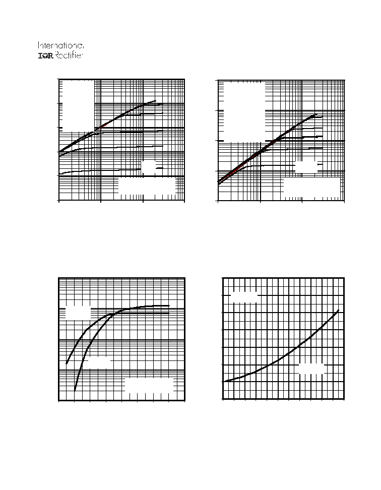
Fig 4. Normalized On-Resistance
Vs. Temperature
Fig 2. Typical Output Characteristics
Fig 1. Typical Output Characteristics
Fig 3. Typical Transfer Characteristics
0.0
0.5
1.0
1.5
2.0
2.5
3.0
3.5
-60 -40 -20
0
20
40 60
80 100 120 140 160
T
J
, Junction Temperature (∞C)
R
DS(on)
, Drain-to-Source On Resistance
(Normalized)
V
GS
=10V
I
D
=24A
0.01
0.1
1
10
100
1000
0.1
1
10
100
V
G S
TO P 15
10
8.0
7.0
6.0
5.5
B O TTO M 5.0
5 V
20 µs PULSE WIDTH
TJ=25∞C
0.1
1
10
100
1000
0.1
1
10
100
V
G S
TO P 15
10
8.0
7.0
6.0
5.5
5.0
B O TTO M 4.5
4.5 V
20 µs PULSE
WIDTH
T 150∞C
I
D
, Drain-to-Source Current (A
)
I
D
, Drain-to-Source Current (A)
V
DS
, Drain-to-Source Voltage (V
)
V
DS
, Drain-to-Source Voltage (V
)
0.1
1
10
100
1000
4
5
6
7
8
9
10
11
12
V
GS
, Gate-to-Source Voltage (V)
I
D
, Drain-to-Source Current (A)
T
J
=150∞C
T
J
=25∞C
V
DS
=20V
20
µ
s PULSE WIDTH
4
www.irf.com
I27139- 01/03
FC40SA50FK
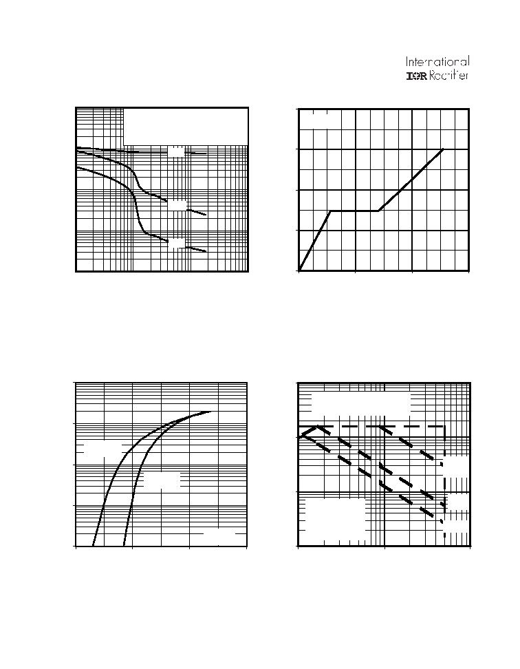
Fig 8. Maximum Safe Operating Area
Fig 6. Typical Gate Charge Vs.
Gate-to-Source Voltage
Fig 5. Typical Capacitance Vs.
Drain-to-Source Voltage
Fig 7. Typical Source-Drain Diode
Forward Voltage
1
10
100
1000
VDS, Drain-to-Source Voltage (V)
10
100
1000
10000
100000
C, Capacitance(pF)
Coss
Crss
Ciss
VGS = 0V, f = 1 MHZ
Ciss = Cgs + Cgd, Cds SHORTED
Crss = Cgd
Coss = Cds + Cgd
0.1
1
10
100
1000
0.2
0.7
1.2
1.7
V
SD
, Source-to-Drain Voltage (V)
I
SD
, Reverse Drain Current (A
)
V
GS
=0
T
J
=150∞C
T
J
=25∞C
0
5
10
15
20
0
100
200
300
Q
G
, Total Gate Charge (nC)
V
GS
, Gate-to-Source Voltage (V)
I
D
=40A
1
10
100
1000
10
100
1000
V
DS
, Drain-to-Source Voltage (V)
I
D
, Drain Current (A)
100us
10ms
1ms
OPERATION IN THIS AREA
LIMITED BY RDS(on)
T
C
= 25∞C
T
J
= 150∞C
Single Pulse

FC40SA50FK
www.irf.com
5
I27139- 01/03
Fig 10a. Switching Time Test Circuit
V
DS
90%
10%
V
GS
t
d(on)
t
r
t
d(off)
t
f
Fig 10b. Switching Time Waveforms
V
DS
Pulse Width
1
µs
Duty Factor
0.1 %
R
D
V
GS
R
G
D.U.T.
10V
+
-
V
DD
Fig 11. Maximum Effective Transient Thermal Impedance, Junction-to-Case
Fig 9. Maximum Drain Current Vs.
Case Temperature
0
10
20
30
40
25
50
75
100
125
150
TC, Case Temperature (∞C)
ID, Drain Current (A)
0.001
0.010
0.100
1.000
0.00001
0.0001
0.001
0.01
0.1
1
t1, Rectangular Pulse Duration (s)
Thermal Response ( ZthJC
SINGLE PULSE
(THERMAL RESPONSE)
0.01
0.02
0.05
0.10
0.30
D = 0.50
Notes:
1. Duty factor D = t1/t2
2. Peak TJ=PDM x ZthJC + TC
Ri (∞C/W)
i (sec)
0.161 0.000759
0.210 0.017991
0.147 0.06094
J
J
1
1
2
2
3
3
R
1
R
1
R
2
R
2
R
3
R
3
C
Ci
i
/
Ri
Ci=
i
/
Ri

6
www.irf.com
I27139- 01/03
FC40SA50FK
Q
G
Q
GS
Q
GD
V
G
Charge
V
GS
V
Fig 13a. Gate Charge Test Circuit
Fig 13b. Basic Gate Charge Waveform
Fig 12a. Maximum Avalanche Energy
Vs. Drain Current
Fig 12d. Unclamped Inductive Waveforms
Fig 12c. Unclamped Inductive Test Circuit
tp
V
(BR)DSS
I
AS
R G
IAS
0.01
tp
D.U.T
L
VDS
+
- VDD
DRIVER
A
15V
20V
0
500
1000
1500
2000
2500
3000
25
50
75
100
125
150
Starting TJ, Junction Tem perature (∞C)
EAS, Single Pulse Avalanche Energy (mJ)
I
D
...
TOP 18A
26A
BOTTOM 40A
1m A
V
GS
-
+
V
DS
D.U.T.
R
L
D
I
FC40SA50FK
www.irf.com
7
I27139- 01/03
P.W.
Period
di/dt
Diode Recovery
dv/dt
Ripple
5%
Body Diode
Forward Drop
Re-Applied
Voltage
Reverse
Recovery
Current
Body Diode Forward
Current
V
GS
=10V
V
DD
I
SD
Driver Gate Drive
D.U.T. I
SD
Waveform
D.U.T. V
DS
Waveform
Inductor Curent
D =
P.W.
Period
+
-
+
+
+
-
-
-
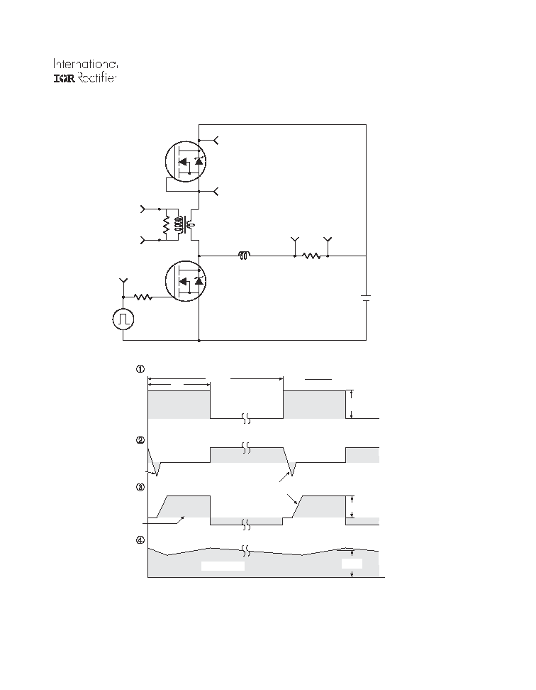
Fig 14. For N-Channel HEXFET
Æ
Power MOSFETs
*
V
GS
= 5V for Logic Level Devices
Peak Diode Recovery dv/dt Test Circuit
#
%
$
R
G
V
DD
∑
dv/dt controlled by R
G
∑
Driver same type as D.U.T.
∑
I
SD
controlled by Duty Factor "D"
∑
D.U.T. - Device Under Test
D.U.T
Circuit Layout Considerations
∑
Low Stray Inductance
∑
Ground Plane
∑
Low Leakage Inductance
Current Transformer
"
*

8
www.irf.com
I27139- 01/03
FC40SA50FK
IR WORLD HEADQUARTERS: 233 Kansas St., El Segundo, California 90245, USA Tel: (310) 252-7105
TAC Fax: (310) 252-7903
Visit us at www.irf.com for sales contact information.01/02
SOT-227 Package Details
QUANTITY PER TUBE IS 10
M4 SREW AND WASHER INCLUDED
Data and specifications subject to change without notice.
This product has been designed and qualified for Industrial
Level.
4.40 (.173 )
4.20 (.165 )
12.50 ( .492 )
7.50 ( .295 )
2.10 ( .082 )
1.90 ( .075 )
30.20 ( 1.189 )
29.80 ( 1.173 )
8.10 ( .319 )
7.70 ( .303 )
4X
15.00 ( .590 )
R FULL
2.10 ( .082 )
1.90 ( .075 )
0.12 ( .005 )
-C-
0.25 ( .010 ) M C A M B M
25.70 ( 1.012 )
25.20 ( .992 )
-B-
6.25 ( .246 )
CHAMFER
2.00 ( .079 ) X 457
-A-
38.30 ( 1.508 )
37.80 ( 1.488 )
12.30 ( .484 )
11.80 ( .464 )
4
1
3
2
LEAD ASSIGMENTS
IGBT
E
C
G
E
S
D
G
S
HEXFET
A1 K2
K1 A2
3
2
4
1
3
2
4
1
HEXFRED
AUX-S
HEXFET
Note :
AUX-S is a low current input
intended for driving purpose only