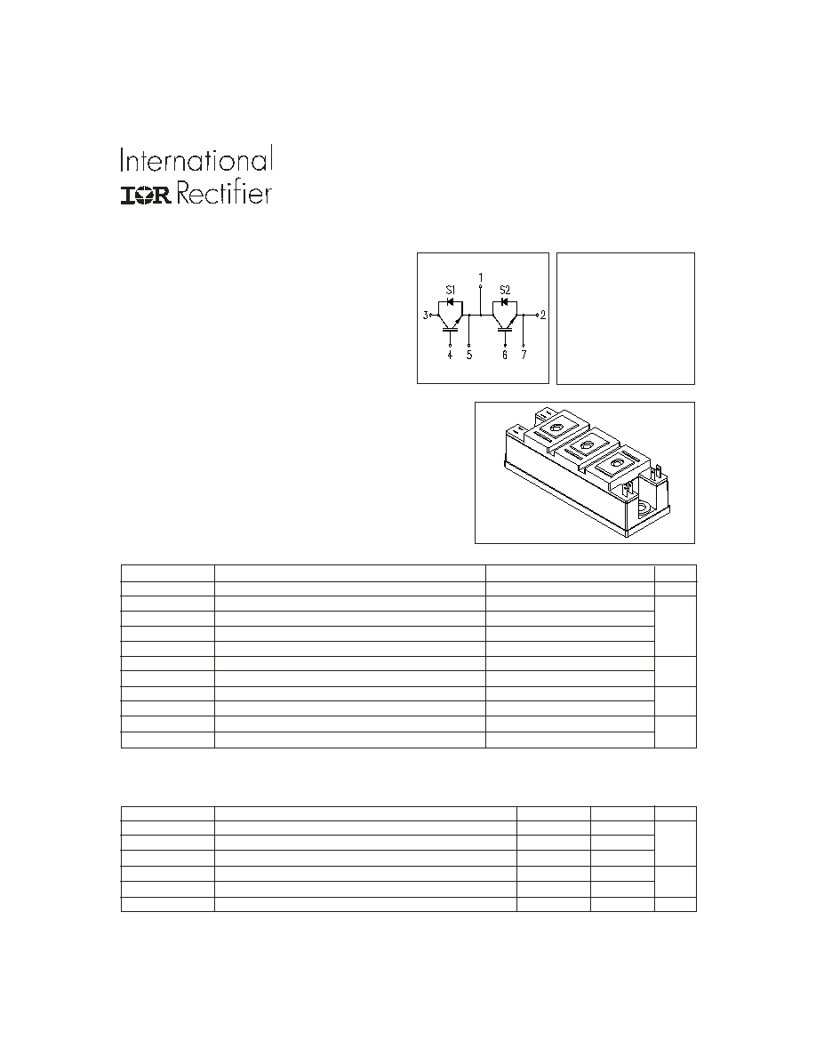
GA250TS60U
"HALF-BRIDGE" IGBT INT-A-PAK
Features
V
CES
=
600
V
V
CE
(on) typ.
= 1.9V
@V
GE
=
15V
,
I
C
=
250A
Parameter
Typ.
Max.
Units
R
JC
Thermal Resistance, Junction-to-Case - IGBT
--
0.16
R
JC
Thermal Resistance, Junction-to-Case - Diode
--
0.35
�C/W
R
CS
Thermal Resistance, Case-to-Sink - Module
0.1
--
Mounting Torque, Case-to-Heatsink
S
--
6.0
N m
Mounting Torque, Case-to-Terminal 1, 2 & 3
T
--
5.0
Weight of Module
200
--
g
Thermal / Mechanical Characteristics
Ultra-Fast
TM
Speed IGBT
Absolute Maximum Ratings
Parameter
Max.
Units
V
CES
Collector-to-Emitter Voltage
600
V
I
C
@ T
C
= 25�C
Continuous Collector Current
250
I
CM
Pulsed Collector Current
Q
500
A
I
LM
Peak Switching Current
R
500
I
FM
Peak Diode Forward Current
500
V
GE
Gate-to-Emitter Voltage
�20
V
V
ISOL
RMS Isolation Voltage, Any Terminal To Case, t = 1 min
2500
P
D
@ T
C
= 25�C
Maximum Power Dissipation
780
W
P
D
@ T
C
= 85�C
Maximum Power Dissipation
400
T
J
Operating Junction Temperature Range
-40 to +150
�C
T
STG
Storage Temperature Range
-40 to +125
� UltraFast: Optimized for high operating
frequencies 8-40 kHz in hard switching, >200
kHz in resonant mode
� Very low conduction and switching losses
� HEXFRED
TM
antiparallel diodes with ultra- soft
recovery
� Industry standard package
� UL approved
Benefits
� Increased operating efficiency
� Direct mounting to heatsink
� Performance optimized for power conversion: UPS,
SMPS, Welding
� Lower EMI, requires less snubbing
� Generation 4 IGBT technology
.
www.irf.com
1
05/14/02
PD - 50047D
GA250TS60U
2
www.irf.com
Parameter
Min. Typ. Max. Units
Conditions
Q
g
Total Gate Charge (turn-on)
--
1050 1600
V
CC
= 400V
Qge
Gate - Emitter Charge (turn-on)
--
146
220
nC
I
C
= 250A
Q
gc
Gate - Collector Charge (turn-on)
--
525
790
T
J
= 25�C
t
d(on)
Turn-On Delay Time
--
173
--
R
G1
= 15
, R
G2
= 0
,
t
r
Rise Time
--
242
--
ns
I
C
= 250A
t
d(off)
Turn-Off Delay Time
--
1020
--
V
CC =
360V
t
f
Fall Time
--
190
--
V
GE
= �15V
E
on
Turn-On Switching Energy
--
10.5
--
mJ
E
off (1)
Turn-Off Switching Energy
--
20.0
--
E
ts (1)
Total Switching Energy
--
30.5
45
C
ies
Input Capacitance
--
23400
--
V
GE
= 0V
C
oes
Output Capacitance
--
1460
--
pF
V
CC
= 30V
C
res
Reverse Transfer Capacitance
--
300
--
= 1 MHz
t
rr
Diode Reverse Recovery Time
--
183
--
ns
I
C
= 250A
I
rr
Diode Peak ReverseCurrent
--
124
--
A
R
G1
= 15
Q
r r
Diode Recovery Charge
--
11275 --
�C
R
G2
= 0
di
(rec)
M
/dt
Diode Peak Rate of Fall of Recovery
--
1700
--
A/�s
V
CC =
360V
During t
b
di/dt
=
1300A/�s
Parameter
Min. Typ. Max. Units
Conditions
V
(BR)CES
Collector-to-Emitter Breakdown Voltage
600
--
--
V
GE
= 0V, I
C
= 1mA
V
CE(on)
Collector-to-Emitter Voltage
--
1.9
2.3
V
GE
= 15V, I
C
= 250A
--
2.0
--
V
V
GE
= 15V, I
C
= 250A, T
J
= 125�C
V
GE(th)
Gate Threshold Voltage
3.0
--
6.0
I
C
= 1.5mA
V
GE(th)
/
T
J
Temperature Coeff. of Threshold Voltage --
-11
--
mV/�C V
CE
= V
GE
, I
C
= 1.5mA
g
fe
Forward Transconductance
T
--
204
--
S
V
CE
= 25V, I
C
= 250A
I
CES
Collector-to-Emitter Leaking Current
--
--
1.0
mA
V
GE
= 0V, V
CE
= 600V
--
--
10
V
GE
= 0V, V
CE
= 600V, T
J
= 125�C
V
FM
Diode Forward Voltage - Maximum
--
4.0
--
V
I
F
= 250A, V
GE
= 0V
--
4.1
--
I
F
= 250A, V
GE
= 0V, T
J
= 125�C
I
GES
Gate-to-Emitter Leakage Current
--
--
250
nA
V
GE
= �20V
Dynamic Characteristics - T
J
= 125�C (unless otherwise specified)
Electrical Characteristics @ T
J
= 25�C (unless otherwise specified)
GA250TS60U
www.irf.com
3
0.1
1
10
100
0
40
80
120
160
200
f, Frequency (KHz)
LOAD CURRENT (A)
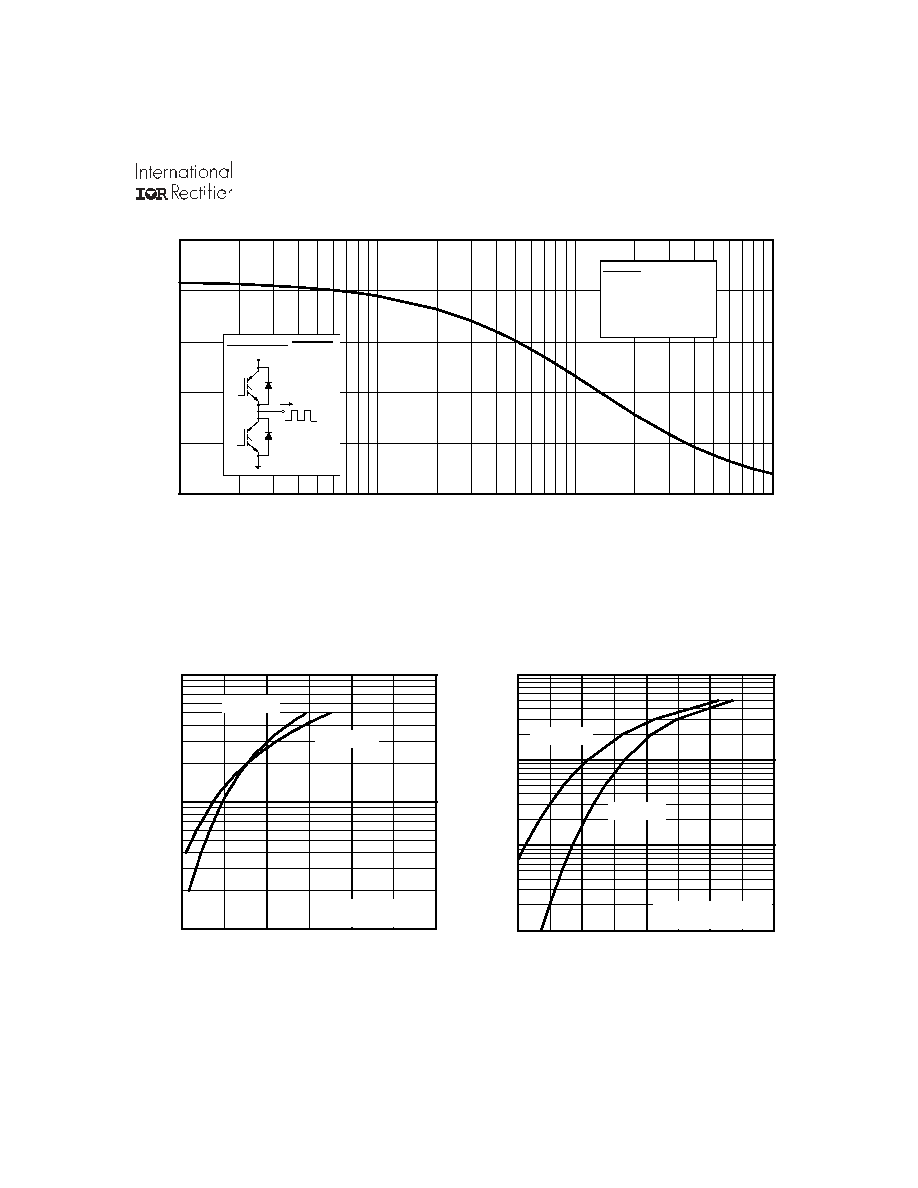
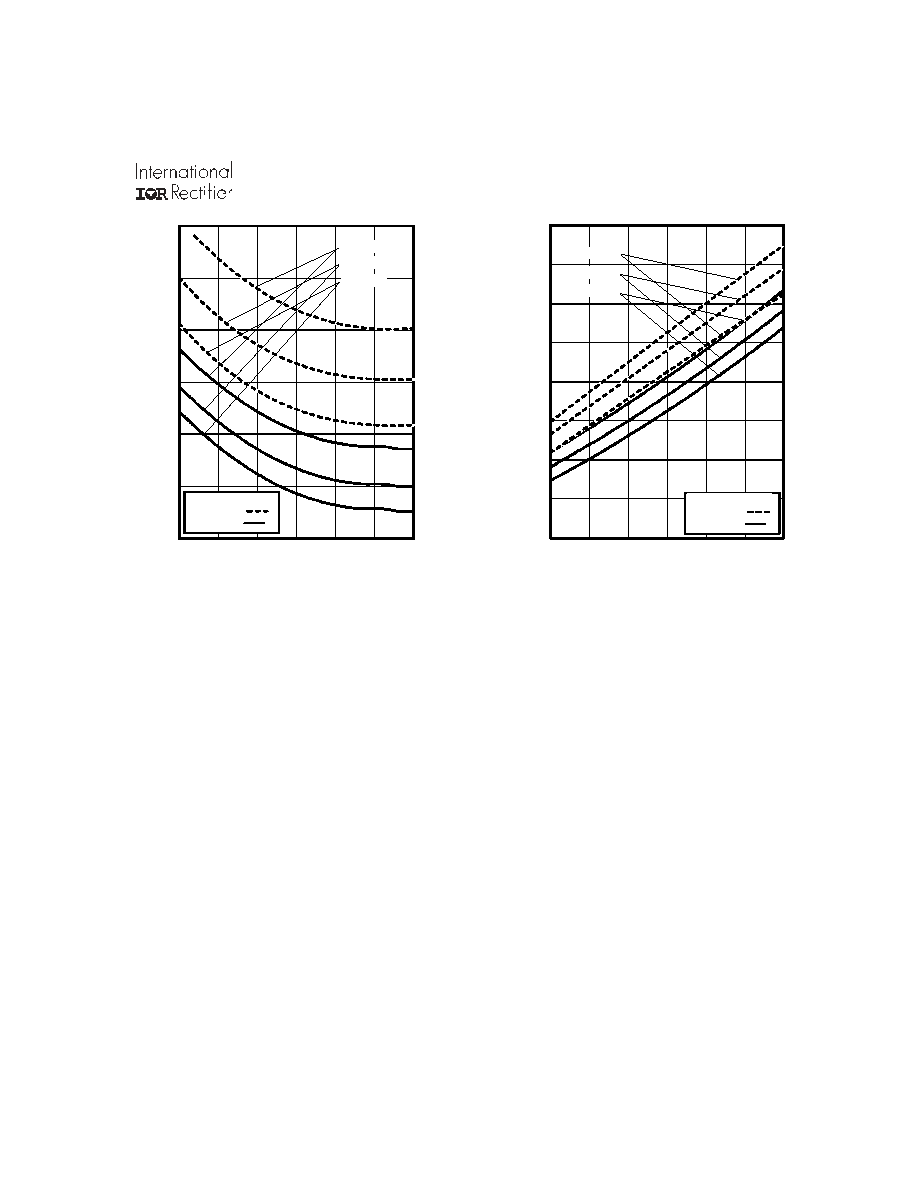
Fig. 1 - Typical Load Current vs. Frequency
(Load Current = I
RMS
of fundamental)
Fig. 2 - Typical Output Characteristics
Fig. 3 - Typical Transfer Characteristics
60 % of ra ted
vo ltag e
I
Id e a l d io d e s
S q u a re w a v e :
F o r b o th :
D u ty c y c le : 5 0 %
T = 1 2 5 � C
T = 9 0 � C
G a te d riv e a s s p e c ifie d
sink
J
P o w e r D is s ip a tio n = W
170
1
10
100
1000
5
6
7
8
9
V , Gate-to-Emitter Voltage (V)
I , Collector-to-Emitter Current (A)
GE
C
V = 50V
5�s PULSE WIDTH
CC
T = 25 C
J
o
T = 150 C
J
o
10
100
1000
1
2
3
4
V , Collector-to-Emitter Voltage (V)
I , Collector-to-Emitter Current (A)
CE
C
V = 15V
20�s PULSE WIDTH
GE
T = 25 C
J
o
T = 150 C
J
o
V
CE
= 25V
80�s PULSE WIDTH
25
25

GA250TS60U
4
www.irf.com
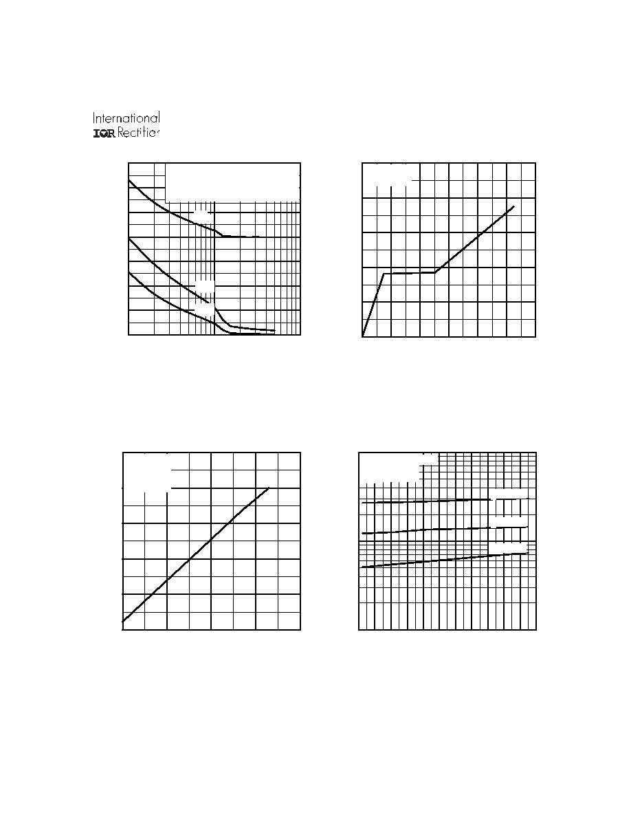
Fig. 6 - Maximum Effective Transient Thermal Impedance, Junction-to-Case
Fig. 5 - Typical Collector-to-Emitter Voltage
vs. Junction Temperature
Fig. 4 - Maximum Collector Current vs. Case
Temperature
-60 -40 -20
0
20
40
60
80 100 120 140 160
1.0
1.2
1.4
1.6
1.8
2.0
2.2
T , Junction Temperature ( C)
V , Collector-to-Emitter Voltage(V)
J
�
CE
V = 15V
80 us PULSE WIDTH
GE
I = A
62.5
C
I = A
125
C
I = A
250
C
25
50
75
100
125
150
0
50
100
150
200
250
T , Case Temperature ( C)
Maximum DC Collector Current(A)
C
�
0 . 0 1
0 . 1
1
0 . 0 0 0 1
0 . 0 0 1
0 . 0 1
0 . 1
1
1 0
1 0 0
1 0 0 0
1
th
J
C
T
h
e
r
m
a
l
R
e
s
p
o
n
s
e
(
Z
)
t , R e cta n g u la r P u ls e D u ra tio n (s e c )
A
S IN G L E P U L S E
( T H E R M A L R E S P O N S E )
D = 0 .5 0
0 .2 0
0 .1 0
0 .0 5
0 .0 2
0 .0 1
P
t 2
1
t
DM
Notes:
1. Duty factor D = t / t
2. Peak T = P x Z + T
1
2
J
DM
thJC
C
GA250TS60U
www.irf.com
5
Fig. 7 - Typical Capacitance vs.
Collector-to-Emitter Voltage
Fig. 8 - Typical Gate Charge vs.
Gate-to-Emitter Voltage
Fig. 9 - Typical Switching Losses vs. Gate
Resistance
Fig. 10 - Typical Switching Losses vs.
Junction Temperature
0
10
20
30
40
20
25
30
35
40
45
R , Gate Resistance (Ohm)
Total Switching Losses (mJ)
G
V = 360V
V = 15V
T = 25 C
I = 250A
CC
GE
J
C
�
-60 -40 -20
0
20
40
60
80 100 120 140 160
1
10
100
T , Junction Temperature ( C )
Total Switching Losses (mJ)
J
�
R = 15Ohm
V = 15V
V = 360V
G
GE
CC
I = A
250
C
I = A
125
C
I = A
62.5
C
125�
R
G1
=15
;R
G2
= 0
1
10
100
0
6000
12000
18000
24000
30000
36000
42000
V , Collector-to-Emitter Voltage (V)
C, Capacitance (pF)
CE
V
C
C
C
=
=
=
=
0V,
C
C
C
f = 1MHz
+ C
+ C
C SHORTED
GE
ies
ge
gc ,
ce
res
gc
oes
ce
gc
Cies
Coes
Cres
0
200
400
600
800
1000
1200
0
4
8
12
16
20
Q , Total Gate Charge (nC)
V , Gate-to-Emitter Voltage (V)
G
GE
V
= 400V
I
= 250A
CC
C

GA250TS60U
6
www.irf.com
Fig. 11 - Typical Switching Losses vs.
Collector-to-Emitter Current
Fig. 12 - Reverse Bias SOA
Fig. 13 - Typical Forward Voltage Drop vs.
Instantaneous Forward Current
0
100
200
300
400
500
0
10
20
30
40
50
60
70
I , Collector-to-emitter Current (A)
Total Switching Losses (mJ)
C
R = 15Ohm
T = 125 C
V = 360V
V = 15V
G
J
CC
GE
�
Fig. 14 - Typical Stored Charge vs. di
f
/dt
0
1 0 0
2 0 0
3 0 0
4 0 0
5 0 0
6 0 0
7 0 0
0
1 0 0
2 0 0
3 0 0
4 0 0
5 0 0
6 0 0
7 0 0
C E
G E
SAFE OPER AT IN G AR EA
V , Collector-to-Em itter Voltage (V)
A
V = 20V
T = 125�C
V m easured at term inal (Peak Voltage)
G E
J
C E
I
C
, Collector-to-Emitter Current ( A )
V
CE
measured at terminal (Peak Voltage)
R
G1
=15
;R
G2
= 0
1 0
1 0 0
1 0 0 0
1.0
2.0
3.0
4.0
5.0
6.0
F M
F
I
n
s
t
ant
a
neous
F
o
r
w
ar
d C
u
r
r
en
t
-
I
(
A
)
F o rw a rd V o lta g e D ro p - V (V )
T = 2 5 �C
T = 1 2 5 �C
J
J
0
5 0 0 0
1 0 0 0 0
1 5 0 0 0
2 0 0 0 0
5 0 0
1 0 0 0
1 5 0 0
2 0 0 0
f
d i /d t - (A /� s)
RR
Q
-
(
n
C
)
I = 50 0A
I = 25 0A
I = 12 5 A
F
F
F
R
J
J
V = 36 0V
T = 1 25 �C
T = 2 5�C
GA250TS60U
www.irf.com
7
Fig. 15 - Typical Reverse Recovery vs. di
f
/dt
Fig. 16 - Typical Recovery Current vs. di
f
/dt
1 0 0
1 5 0
2 0 0
2 5 0
5 0 0
1 0 0 0
1 5 0 0
2 0 0 0
t
r
r
-
(n
s
)
f
d i /d t - (A /� s )
I = 5 00A
I = 2 50A
I = 125A
F
F
F
R
J
J
V = 3 6 0 V
T = 1 2 5 �C
T = 2 5 � C
0
5 0
1 0 0
1 5 0
2 0 0
5 0 0
1 0 0 0
1 5 0 0
2 0 0 0
f
d i /d t - (A /� s)
RR
M
I
-
(
A
)
I = 500A
I = 250A
I = 12 5A
F
F
F
R
J
J
V = 3 6 0 V
T = 1 2 5 �C
T = 2 5 � C
GA250TS60U
8
www.irf.com
t1
Ic
V c e
t1
t2
9 0 % Ic
1 0 % V c e
td (o ff)
tf
Ic
5 % Ic
t1 + 5 � S
V c e ic d t
9 0 % V g e
+ V g e
E o f f =
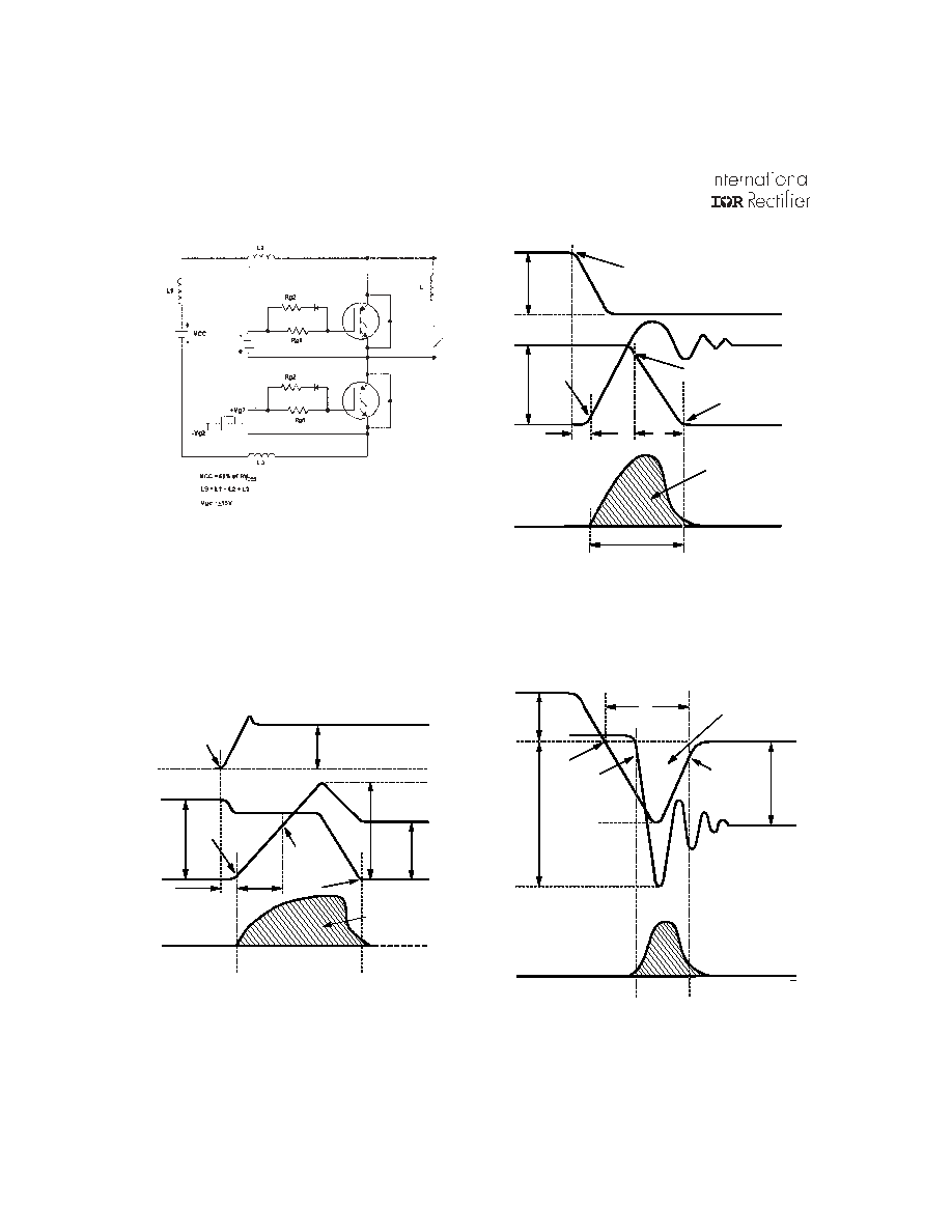
Fig. 17b -
Test Waveforms for Circuit of Fig. 18a, Defining
E
off
, t
d(off)
, t
f
V ce ie d t
t2
t1
5 % V c e
Ic
Ip k
V c c
1 0 % Ic
V c e
t1
t2
D U T V O L T A G E
A N D C U R R E N T
G A T E V O L T A G E D .U .T .
+ V g
1 0 % +V g
9 0 % Ic
tr
td (o n )
D IO D E R E V E R S E
R E C O V E R Y E N E R G Y
tx
E o n =
E re c =
t4
t3
V d id d t
t4
t3
D IO D E R E C O V E R Y
W A V E F O R M S
Ic
V p k
1 0 % V c c
Irr
1 0 % Irr
V cc
trr
Q rr =
trr
tx
id d t
Fig. 17a -
Test Circuit for Measurement of
I
LM
, E
on
, E
off(diode)
, t
rr
, Q
rr
, I
rr
, t
d(on)
, t
r
, t
d(off)
, t
f
Fig. 17c -
Test Waveforms for Circuit of Fig. 18a,
Defining E
on
, t
d(on)
, t
r
Fig. 17d -
Test Waveforms for Circuit of Fig. 18a,
Defining E
rec
, t
rr
, Q
rr
, I
rr
Vd Ic dt
Vce Ic dt
Ic dt
Vce Ic dt
GA250TS60U
www.irf.com
9
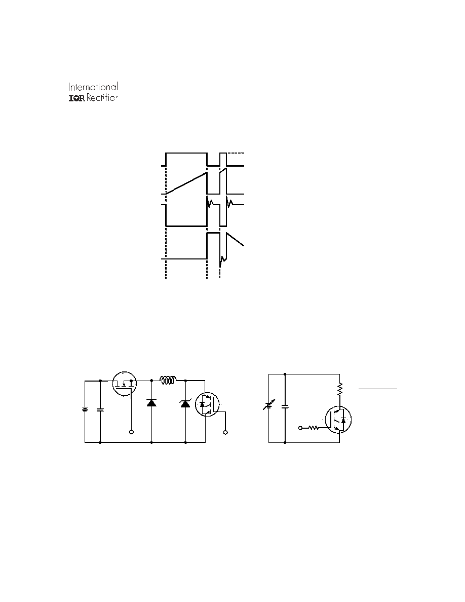
V g
G A T E S IG N A L
D E V IC E U N D E R T E S T
C U R R E N T D .U .T .
V O L T A G E IN D .U .T .
C U R R E N T IN D 1
t0
t1
t2
D . U . T .
V *
c
5 0 V
L
1 0 0 0 V
6 0 0 0 � F
1 0 0 V
Figure 18. Clamped Inductive Load Test Circuit
Figure 19. Pulsed Collector Current
Test Circuit
R
L
=
480V
4 X I
C
@25�C
0 - 480V
Figure 17e. Macro Waveforms for
Figure 18a's
Test Circuit
GA250TS60U
10
www.irf.com
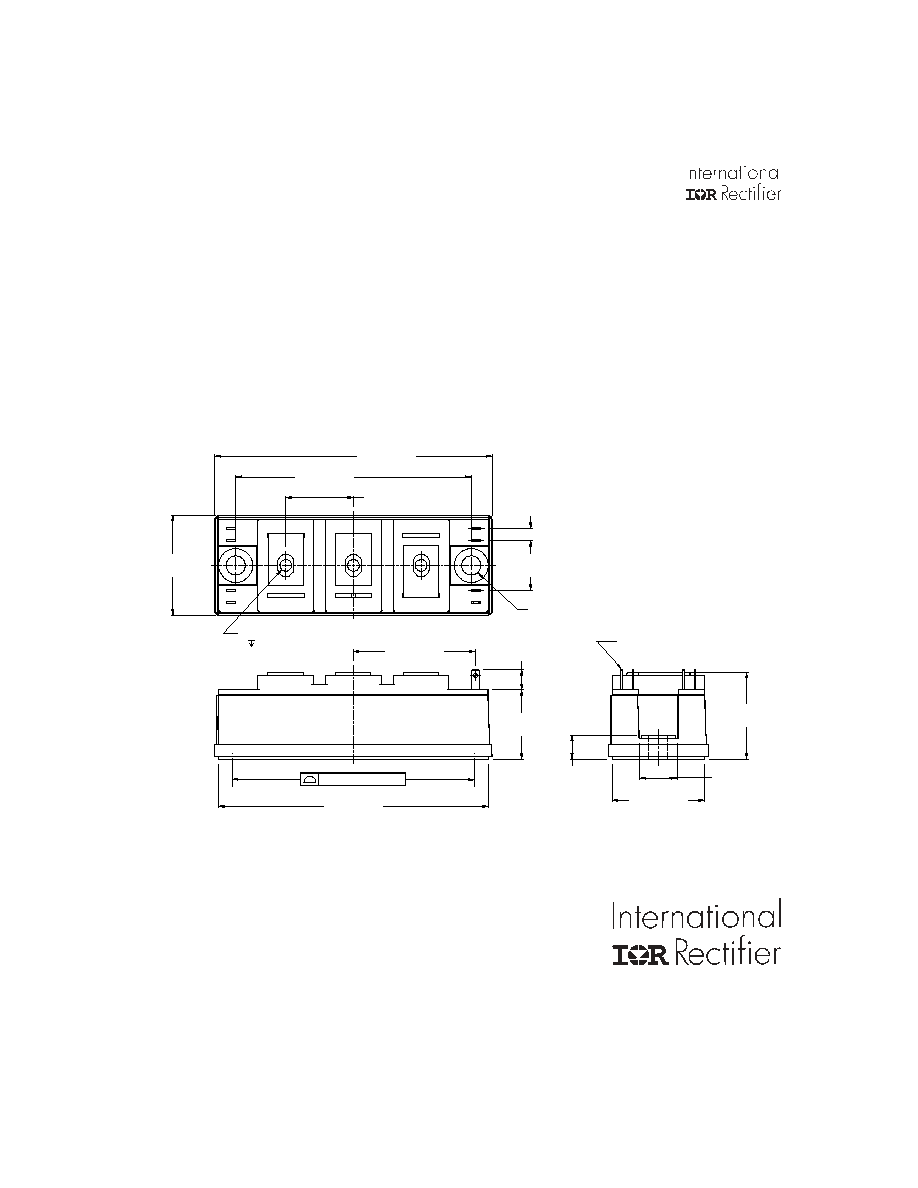
Case Outline -- INT-A-PAK
Notes:
Q
Repetitive rating; V
GE
= 20V, pulse width limited by
max. junction temperature.
R
See fig. 17
S
For screws M6.
T
For screws M5.
U
Pulse width 50�s; single shot.
Data and specifications subject to change without notice.
This product has been designed and qualified for the Industrial market.
Qualification Standards can be found on IR's Web site.
IR WORLD HEADQUARTERS: 233 Kansas St., El Segundo, California 90245, USA Tel: (310) 252-7105
TAC Fax: (310) 252-7903
Visit us at www.irf.com for sales contact information.05/02
9
8
10
11
4
5
7
6
3
2
1
1. ALL DIMENS IONS ARE S HOWN IN MILLIMET ERS [INCHES ].
2. CONT ROLLING DIMENS ION: MILLIMET ER.
NOT ES :
4X FAS T ON T AB (110)
2.8 x 0.5 [.110 x .020]
3X M5
8 [.314]
MAX.
2X �
6.80
6.20
[
.267
.244
]
4.50
3.50
[
.177
.138
]
32.00
31.00
[
1.260
1.220
]
24.00
23.00
[
.945
.906
]
30.50
29.00
[
1.201
1.142
]
92.10
91.10
[
3.626
3.587
]
8.00
6.60
[
.315
.260
]
8.65
7.65
[
.341
.301
]
94.70
93.70
[
3.728
3.689
]
2X
23.50
22.50
[
.925
.886
]
80.30
79.70
[
3.161
3.138
]
17.50
16.50
[
.689
.650
]
42.00
41.00
[
1.654
1.614
]
34.70
33.70
[
1.366
1.327
]
2X
13.30
12.70
[
.524
.500
]
0.15 [.0059] CONVEX