 | ÐлекÑÑоннÑй компоненÑ: IP2003 | СкаÑаÑÑ:  PDF PDF  ZIP ZIP |
Äîêóìåíòàöèÿ è îïèñàíèÿ www.docs.chipfind.ru
www.irf.com
1
iP2003
Features:
Full function multiphase building block
Output current 40A continuous with no derating up to
T
PCB
= 100°C and T
CASE
= 100°C
Operating frequency up to 1.0 MHz
Efficient dual sided cooling
Small footprint low profile (11mm x 11mm x 2.2mm) package
Optimized for very low power losses
LGA interface
Ease of design
Proprietary packaging enables ultra low Rth
j-case top
Synchronous Buck
Multiphase Optimized LGA Power Block
Integrated Power Semiconductors, Drivers & Passives
Description
The iP2003 is a fully optimized solution for high current synchronous buck multiphase applications.
Board space and design time are greatly reduced because most of the components required for each
phase of a typical discrete-based multiphase circuit are integrated into a single 11mm x 11mm x 2.2mm
power block. The only additional components required for a complete multiphase converter are a PWM IC, the
external inductors, and the input and output capacitors.
iPOWIR technology offers designers an innovative board space saving solution for applications
requiring high power densities. iPOWIR technology eases design for applications where component integration
offers benefits in performance and functionality. iPOWIR technology solutions are also optimized internally for
layout, heat transfer and component selection.
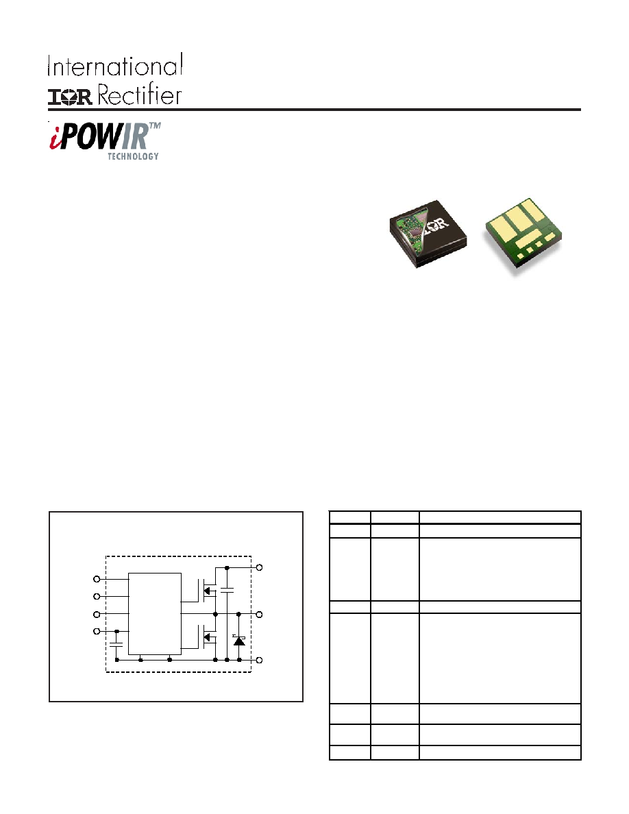
iP2003 Power Block
11/18/04
iP2003 Internal Block Diagram
MOSFET
Driver with
dead time
control
V
IN
V
SW
PGND
PRDY
ENABLE
PWM
V
DD
SGND
MOSFET
Driver with
dead time
control
V
IN
V
SW
PGND
PRDY
ENABLE
PWM
V
DD
SGND
PD- 96922A
Pin #
Pin Name Pin Function
1
V
DD
Supply voltage for the internal circuitry.
2
ENABLE
When set to logic level high, internal circuitry
of the device is enabled. When set to logic
level low, the PRDY pin is forced low, the
Control and Sychronous switches are turned
off, and the supply current is less than 10µA.
3
PWM
TTL-level input signal to MOSFET drivers.
4
PRDY
Power Ready - This pin indicates the status of
ENABLE or V
DD
. This output will be driven
low when ENABLE is logic low or when V
DD
is less than 4.4V (typ.). When ENABLE is
logic high and V
DD
is greater than 4.4V (typ.),
this output is driven high. This output has a
10mA source and 1mA sink capability.
5, 7
PGND
Power Ground - connection to the ground of
bulk and filter capacitors.
6
V
SW
Switching Node - connection to the output
inductor.
8
V
IN
Input voltage for the DC-DC converter.

www.irf.com
2
iP2003
Measurement were made using four 10uF (TDK C3225X5R1C106KT or equiv.) capacitors across the input (see
Fig. 8).
Not associated with the rise and fall times. Does not affect Power Loss (see Fig. 9).
All specifications @25°C (unless otherwise specified)
Absolute Maximum Ratings:
Parameter
Symbol
Min
Typ
Max
Units
Conditions
V
IN
to PGND
V
IN
-
-
16
V
V
DD
to PGND
V
DD
-
-
6.0
V
PWM to PGND
PWM
-0.3
-
V
DD
+0.3
V
Not to exceed 6.0V
Enable to PGND
ENABLE
-0.3
-
V
DD
+0.3
V
Not to exceed 6.0V
Output RMS Current
I
OUT
-
-
40
A
Measured at V
SW
Block Temperature
T
BLK
-40
-
125
°C
Capable of start up over full
temperature range
Recommended Operating Conditions:
Parameter
Symbol
Min
Typ
Max
Units
Conditions
Supply Voltage
V
DD
4.6
5.0
5.5
V
Input Voltage
V
IN
3.0
-
13.2
V
Output Voltage
V
OUT
0.8
-
3.3
V
Output Current
I
OUT
-
-
40
A
Operating Frequency
fsw
300
-
1000
kHz
Operating Duty Cycle
D
-
-
85
%
Electrical Specifications @ V
DD
= 5V (unless otherwise specified):
Parameter
Symbol
Min
Typ
Max
Units
Conditions
Block Power Loss
c
P
LOSS
-
9.4
11.7
W
V
IN
=12V, V
OUT
=1.3V
Turn On Delay
d
t
d(on)
-
63
-
I
OUT
=40A, f
SW
=1MHz
Turn Off Delay
d
t
d(off)
-
26
-
L = 0.3µH
V
IN
Quiescent Current
I
Q-VIN
-
-
1.0
mA
Enable = 0V, V
IN
=12V
V
DD
Quiescent Current
I
Q-VDD
-
10
-
µA
Enable = 0V, V
DD
=5V
Under-Voltage Lockout
UVLO
Start Threshold
V
START
4.2
4.4
4.5
V
Hysteresis
V
Hvs-UVLO
-
150
-
mV
Enable
ENABLE
Input Voltage High
V
IH
2.0
-
-
V
Input Voltage Low
V
IL
-
-
0.8
Power Ready
PRDY
Logic Level High
V
OH
4.5
4.6
-
V
V
DD
=4.6V, I
Load
=10mA
Logic Level Low
V
OL
-
0.1
0.2
V
DD
<UVLO Threshold, I
Load
= 1mA
PWM Input
PWM
Logic Level High
V
OH
2.0
-
-
V
Logic Level Low
V
OL
-
-
0.8
ns
www.irf.com
3
iP2003
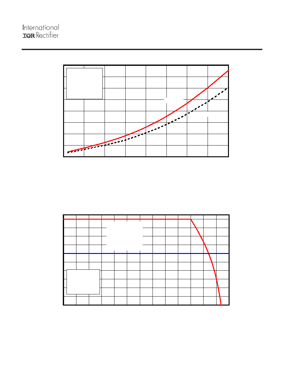
Fig. 1: Power Loss vs. Current
Fig. 2: Safe Operating Area (SOA) vs. T
PCB
& T
CASE
0
10
20
30
40
50
60
70
80
90
100
110
120
130
Case Temperature (°C)
0
5
10
15
20
25
30
35
40
Output Current (A)
0
2
4
6
8
10
12
14
16
P
o
w
e
r
L
o
s
s
(
W
)
Maximum
Typical
VIN = 12V
VOUT = 1.3V
fsw = 1MHz
TBLK = 125°C
L = 0.30µH
0
10
20
30
40
50
60
70
80
90
100
110
120
130
PCB Temperature (°C)
0
4
8
12
16
20
24
28
32
36
40
O
u
t
p
u
t
C
u
r
r
e
n
t
(
A
)
Safe
Operating
Area
VIN = 12V
VOUT = 1.3V
fsw = 1MHz
L = 0.30µH
Tx

www.irf.com
4
iP2003
Fig. 7: I
DD
(V
DD
current) vs. Frequency
Fig. 5: Normalized Power Loss vs. Frequency
Fig. 3: Normalized Power Loss vs. V
IN
Fig. 4: Normalized Power Loss vs. V
OUT
Typical Performance Curves
Fig. 6: Normalized Power Loss vs. Inductance
3
4
5
6
7
8
9
10
11
12
13
Input Voltage (V)
-1
0
1
2
3
4
5
6
7
S
O
A
T
e
m
p
A
d
j
u
s
t
m
e
n
t
(
°
C
)
0.96
1.00
1.04
1.08
1.12
1.16
1.20
1.24
1.28
P
o
w
e
r
L
o
s
s
(
N
o
r
m
a
l
i
z
e
d
)
VOUT = 1.3V
IOUT = 40A
fsw = 1MHz
L = 0.3µH
TBLK = 125°C
200
300
400
500
600
700
800
900 1000
Swiching Frequency (kHz)
0.65
0.70
0.75
0.80
0.85
0.90
0.95
1.00
1.05
P
o
w
e
r
L
o
s
s
(
N
o
r
m
a
l
i
z
e
d
)
-7.0
-6.0
-5.0
-4.0
-3.0
-2.0
-1.0
0.0
1.0
S
O
A
T
e
m
p
A
d
j
u
s
t
m
e
n
t
(
°
C
)
VIN = 12V
VOUT = 1.3V
IOUT = 40A
L = 0.30µH
TBLK = 125°C
0.1
0.3
0.5
0.7
0.9
Output Inductance (µH)
0.98
1.00
1.02
1.04
1.06
P
o
w
e
r
L
o
s
s
(
N
o
r
m
a
l
i
z
e
d
)
-0.5
0.0
0.5
1.0
1.5
S
O
A
T
e
m
p
A
d
j
u
s
t
m
e
n
t
(
°
C
)
VIN = 12V
VOUT = 1.3V
IOUT = 40A
fsw = 1MHz
TBLK = 125°C
250
500
750
1000
Switching Frequency (kHz)
20
30
40
50
60
70
80
Aver
age I
DD (
mA
)
Does not include
PRDY current
TBLK = 25°C
0.8
1.2
1.6
2.0
2.4
2.8
3.2
3.6
Output Voltage (V)
0.96
1.00
1.04
1.08
1.12
1.16
P
o
w
e
r
L
o
s
s
(
N
o
r
m
a
l
i
z
e
d
)
-1.0
0.0
1.0
2.0
3.0
4.0
S
O
A
T
e
m
p
A
d
j
u
s
t
m
e
n
t
(
°
C
)
VIN = 12V
IOUT = 40A
fsw = 1MHz
L = 0.30µH
TBLK = 125°C

www.irf.com
5
iP2003
Applying the Safe Operating Area (SOA) Curve
The SOA graph incorporates power loss and thermal resistance information in a way that allows one to solve for maximum
current capability in a simplified graphical manner. It incorporates the ability to solve thermal problems where heat is drawn
out through the printed circuit board and the top of the case.
Procedure
1) Draw a line from Case Temp axis at T
CASE
to the PCB
Temp axis at T
PCB
.
2) Draw a vertical line from the T
X
axis intercept to the SOA
curve.
3) Draw a horizontal line from the intersection of the vertical
line with the SOA curve to the Y-axis. The point at which
the horizontal line meets the Y-axis is the SOA current.
Calculating Power Loss and SOA for Different Operating Conditions
To calculate power loss for a given set of operating conditions, the following procedure should be followed:
Determine the maximum current for each iP2003 and obtain the maximum power loss from Fig 1. Use the curves in
Figs. 3, 4, 5 and 6 to obtain normalized power loss values that match the operating conditions in the application. The
maximum power loss under the operating conditions is then the product of the power loss from Fig. 1 and the normal-
ized values.
To calculate the SOA for a given set of operating conditions, the following procedure should be followed:
Determine the maximum PCB temperature and Case temperature at the maximum operating current of each iP2003.
Obtain the SOA temperature adjustments that match the operating conditions in the application from Figs. 3, 4, 5 and
6. Then, add the sum of the SOA temperature adjustments to the Tx axis intercept in Fig 2.
The example below explains how to calculate maximum power loss and SOA.
Example:
Operating Conditions
Output Current = 40A
Input Voltage = 10V
Output Voltage = 3.3V
Sw Freq= 900kHz
Inductor = 0.2µH T
PCB
= 100°C, T
CASE
= 110°C
Calculating Maximum Power Loss:
(Fig. 1)
Maximum power loss
=
15W
(Fig. 3)
Normalized power loss for input voltage
0.98
(Fig. 4)
Normalized power loss for output voltage
1.14
(Fig. 5)
Normalized power loss for frequency
0.94
(Fig. 6)
Normalized power loss for inductor value
1.013
Calculated Maximum Power Loss for given conditions = 15W x 0.98 x 1.14 x 0.94 x 1.013
15.96W
120
10
20
30
40
50
60
70
80
90
100
110
0
0
2
4
6
8
10
12
14
16
18
20
22
24
26
28
30
32
34
36
38
40
42
0
10
20
30
40
50
60
70
80
90
100
110
120
PCB Temperature (ºC)
Output C
u
r
r
e
nt (A
)
Safe
Operating
Area
V
IN
= 12V
V
OUT
= 1.3V
f
SW
= 1MHz
L=0.3uH
Case Temperature (ºC
)
T
X