Äîêóìåíòàöèÿ è îïèñàíèÿ www.docs.chipfind.ru

Description
The IR062HD4C10U-P2 / IR082HD4C10U-P2 are
high voltage, high speed half bridges. Proprietary
HVIC and latch immune CMOS technologies,
along with the power IGBT technology, enable
ruggedized single package construction. The
logic inputs are compatible with standard CMOS
or LSTTL outputs, down to 3.3V logic. The front-
end features an independent high and low side
driver in phase with the logic compatible input
signals. The output features two IGBT's in a half-
bridge configuration. Propagation delays for the
high and low side power IGBT's are matched to
simplify use. The device can operate up to 575 volts.
Package
Product Summary
V
IN
(max)
575V
P
D
(T
A
= 25
)
3.0W
V
CE(ON)
typ
3.0V
°
C
7 Pin
HIGH VOLTAGE HALF BRIDGE
Preliminary Data Sheet No. PD60171-D
IR062HD4C10U-P2
IR082HD4C10U-P2
www.irf.com
1
Features
·
Output Power IGBT's in half-bridge configuration
·
575V rated breakdown voltage
·
High side gate drive designed for bootstrap
operation
·
Matched propagation delay for both channels
·
Independent high and low side output channels
(IR062HD4C10U-P2) or cross-conduction
prevention logic (IR082HD4C10U-P2)
·
Undervoltage lockout
·
3.3V, 5V and 15V input logic compatible
·
Metal heatsink back for improved PD
2
www.irf.com
IR062HD4C10U-P2
IR082HD4C10U-P2
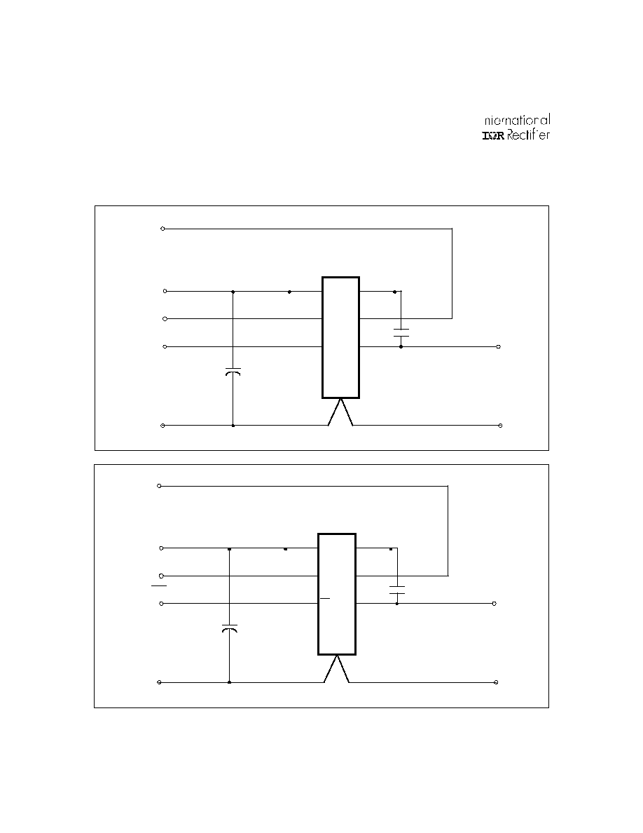
Typical Connections
Please note this info sheet contains advance information which may change before the product is released to production.
Please note this info sheet contains advance information which may change before the product is released to production.
V I N
C O M
H
IN
1
2
3
4
6
7
9
V c c
C O M
V O
V
I N
V
B
T O
L O A D
H V D C B u s
H
I N
L
I N
V c c
L
IN
IR062HD4C10U-P2
V I N
C O M
H
IN
1
2
3
4
6
7
9
V c c
C O M
V O
V
I N
V
B
T O
L O A D
H V D C B u s
H
I N
L
I N
V c c
L
IN
IR082HD4C10U-P2

www.irf.com
3
IR062HD4C10U-P2
IR082HD4C10U-P2
Note 1:
Logic operational for VO of -5 to 575V. Logic state held for VO of -5 to -V
BO
Recommended Operating Conditions
The Input/Output logic timing diagram is shown in Figure 1. For proper operation the device should be used within the
recommended conditions.
Symbol
Definition
Min.
Max.
Units
V
B
High side floating supply absolute voltage
V
O
+ 10
V
O
+ 20
V
IN
High voltage supply
--
575
V
O
Half-bridge output voltage
(note 1)
V
IN
V
CC
Low side and logic fixed supply voltage
10
20
V
IH/
V
IL
Logic input voltage (HIN & LIN)
0
V
CC
T
A
Ambient temperature
-40
125
I
C
Continuous collector current (TC = 25 °C)
--
2.0
(TC = 85 °C)
----
1.1
A
V
Absolute Maximum Ratings
Absolute Maximum Ratings indicate sustained limits beyond which damage to the device may occur. All voltage param-
eters are absolute voltages referenced to COM, all currents are defined positive into any lead. The Thermal Resistance
and Power Dissipation ratings are measured under board mounted and still air conditions.
Symbol
Definition
Min.
Max.
Units
V
IN
High voltage supply
- 0.3
575
V
B
High side floating supply absolute voltage
VO -0.3
VO+ 25
VO
Half-bridge output voltage
-0.3
V
IN
+ 0.3
V
V
IH/
V
IL
Logic input voltage (HIN & LIN)
- 0.3
V
cc
+ 0.3
V
CC
Low side and logic fixed supply voltage
-0.3
25
V
dV/dt
Peak diode recovery dv/dt
--
3.50
V/ns
P
D
Package power dissipation @ T
A
+25°C
--
3.00
W
Rth
JA
Thermal resistance, junction to ambient
--
50
Rth
Jc
Thermal resistance, junction to case (metal)
--
20
T
J
Junction temperature
-55
150
T
S
Storage temperature
-55
150
T
L
Lead temperature (soldering, 10 seconds)
--
300
V
°C/W
°C

4
www.irf.com
IR062HD4C10U-P2
IR082HD4C10U-P2
8.0 8.9
9.8 V
7.4 8.2
9.0 V
TA = 25
o
C
Symbol
Definition Min. Typ. Max. Units Test Conditions
V
CCUV+
V
CC
supply undervoltage positive going
V
BSUV+
threshold
V
CCUV-
V
CC
supply undervoltage negative going
V
BSUV-
threshold
I
QCC
Quiescent V
CC
supply current
0.4
1.0
1.6
mA
I
QBO
Quiescent V
BO
supply current
20
60
150
I
LK
Offset supply leakage current
@25°C
--
--
100
V
B
= 575V
I
INLK
Vin to VO leakage current
@25°C
--
--
250
@150°C
--
1000
--
I
OLK
VO leakage current
@25°C
--
--
250
@150°C
--
1000
--
V
IH
Logic "1" input voltage
2.7
--
--
V
IL
Logic "0" input voltage
--
--
0.8
I
IN+
Logic "1" input bias current
--
20
40
I
IN-
Logic "0" input bias current
--
--
1
V
CE
(on)
Collector-to-Emitter saturation voltage
--
3.0
--
IC = 400mA
V
EC
Diode forward voltage
--
1.2
--
IE = 400mA
VF
Bootstrap Diode forward voltage (D1)
--
1.5
--
IF = 400mA
Static Electrical Characteristics
V
BIAS
(V
CC
, V
BS
) = 15V and T
A
= 25°C unless otherwise specified. The V
IN
and I
IN
parameters are referenced to COM.
V
µA
V
V
IN
= 5V
µA
V
IN
= 575V,
VO = 0V
V
CC
= 10V to 20V
V
O
= 575V
V
Dynamic Electrical Characteristics
V
BIAS
(V
CC
, V
BS
) = 15V and T
A
= 25°C unless otherwise specified. Switching time waveform definitions are shown in
figure 2. Refer to IC data sheets (IR2106 and IR2108) for further characteristics.
Symbol
Definition
Min. Typ. Max. Units Test Conditions
t
on
Turn-on propagation delay (see note 2)
-IR062
--
220
310
Vo = 0V
-IR082
--
680
900
t
off
Turn-off propagation delay (see note 2)
-IR062
--
257
380
Vo = 575V
-IR082
--
220
400
t
rr
Reverse recovery time (FRED Diode)
--
28
--
I
F
= 400mA
Qrr
Reverse recovery charge (FRED Diode)
--
40
--
nC
di/dt
= 100 A/us
Note 2: Switching times as specified and illustrated in figure 2 are referenced to the VO output voltage.
This is shown as VO in figure 2.
ns

www.irf.com
5
IR062HD4C10U-P2
IR082HD4C10U-P2
Lead Assignments
1
Vcc
2
HIN
3
LIN
4
COM
6 VB
7 VO
9 VIN
9
7
6
4
3
2
1
Lead Definitions
Lead
Symbol
Definition
V
CC
Logic and internal gate drive supply voltage.
HIN
Logic input for high side half bridge output, in phase
LIN
Logic input for low side half bridge output, in phase (IR062xxx) or out of phase (IR082xxx)
V
B
High side gate drive floating supply
VIN
High voltage supply
VO
Half bridge output
COM
Logic return and half bridge return
Functional Block Diagram
I R 2 1 0 6
D 1
VIN
V
B
C O M
V O
V c c
H
IN
L
IN
1
2
3
4
6
7
9
H
O
V
S
L
O
F R E D 0 6
F R E D 0 6
I G B T 1
I G B T 1
I R 0 6 2 H 4 C 1 0 U - P 2
I R 2 1 0 8
D 1
VIN
V
B
C O M
V O
V c c
H
IN
L
IN
1
2
3
4
6
7
9
H
O
V
S
L
O
F R E D 0 6
F R E D 0 6
I G B T 1
I G B T 1
I R 0 8 2 H 4 C 1 0 U - P 2