*Please note that this data sheet contains advanced information that could change before the product is released to production.
Features
Secondary side high speed SR controller
DCM, CrCM and CCM flyback topologies
200V proprietary IC technology
Max 500KHz switching frequency
Anti-bounce logic and UVLO protection
7A peak turn off drive current
Micropower start-up &
ultra low quiescent current
10.7/14.5V gate drive clamp
SmartRectifier
TM
CONTROL IC
IR1167ASPbF
IR1167BSPbF
www.irf.com
1
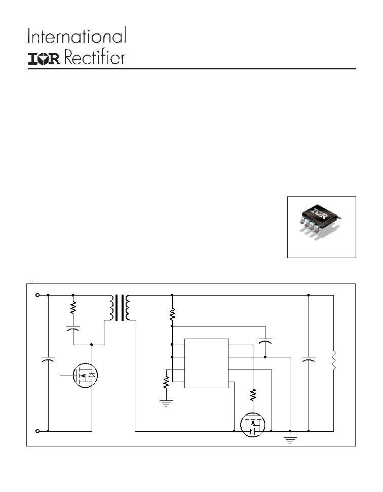
IR1167 Application Diagram
Data Sheet PD60254A
Description
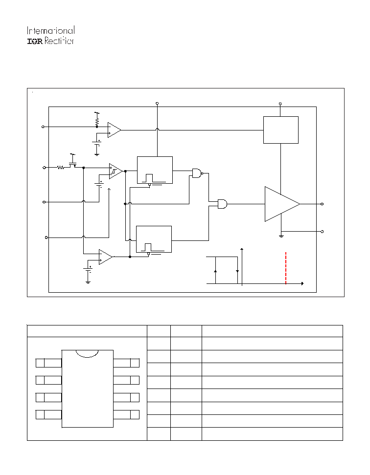
IR1167S is a smart secondary side driver IC designed to drive N-Channel power MOSFETs
used as synchronous rectifiers in isolated Flyback converters.
The IC can control one or more paralleled N-MOSFETs to emulate the behavior of Schottky
diode rectifiers. The drain to source voltage is sensed differentially to determine the polarity
of the current and turn the power switch on and off in proximity of the zero current transi-
tion.
Ruggedness and noise immunity are accomplished using an advanced blanking scheme
and double-pulse suppression which allow reliable operation in continuous, discontinuous
and critical current mode operation and both fixed and variable frequency modes.
Package
8-Lead SOIC
50ns turn-off propagation delay
Vcc range from 11.3V to 20V
Direct sensing of MOSFET drain voltage
Minimal component count
Simple design
Lead-free
Compatible with 1W Standby, Energy Star, CECP, etc.
RMOT
Cdc
Rg
VD
5
VS
6
MOT
3
OVT
2
EN
4
GND
7
VGATE
8
VCC
1
U1
IR1167S
Q1
XFM
Co
LO
AD
Rdc
Vin
Rtn
Ci
Rs
Cs
PRELIMINARY
IR1167AS/BS
PRELIMINARY
www.irf.com
2
* Per EIA/JESD22-A114-B( discharging a 100pF capacitor through a 1.5k series resistor).
Stress beyond those listed under Absolute Maximum Ratings may cause permanent damage to the device.
These are stress ratings only and functional operation of the device at these or any other conditions beyond those
indicated in the operational sections of the specifications are not implied. All voltages are absolute voltages referenced
to GND. Thermal resistance and power dissipation are measured under board mounted and still air conditions.
Absolute Maximum Ratings
Parameters
Symbol
Min.
Max.
Units
Supply Voltage
V
CC
-0.3
20
V
Enable Voltage
V
EN
-0.3
20
V
Cont. Drain Sense Voltage
V
D
-3
200
V
Pulse Drain Sense Voltage
V
D
-5
200
V
Source Sense Voltage
V
S
-3
20
V
Gate Voltage
V
GATE
-0.3
20
V
Operating Junction Temperature
T
J
-40
150
°C
Storage Temperature
T
S
-55
150
°C
Thermal Resistance
R
JA
128
°C/W
Package Power Dissipation
P
D
970
mW
ESD Protection
V
ESD
2
kV
Switching Frequency
fsw
500
kHz
Recommended Operating Conditions
Recommended operating conditions for reliable operation with margin
Parameters
Symbol
Min.
Max.
Units
Supply Voltage
V
CC
12
18
V
Operating Junction Temperature
T
J
-25
125
°C
Ambient Temperature
T
A
-25
85
°C
Switching Frequency
fsw
40
400
kHz
Remarks
Remarks
V
CC
=20V, Gate off
SOIC-8
SOIC-8, T
AMB
=25°C
Human Body Model*
www.irf.com
3
IR1167AS/BS
PRELIMINARY
Electrical Characteristics
The electrical characteristics involve the spread of values guaranteed within the specified supply voltage and
junction temperature range T
J
from 25° C to 125°C. Typical values represent the median values, which are
related to 25°C. If not otherwise stated, a supply voltage of V
CC
=15V is assumed for test condition.
Supply Section
Parameters
Symbol
Min.
Typ.
Max.
Units
V
CC
Turn On Threshold
V
CC ON
9.8
10.5
11.3
V
V
CC
Turn Off Threshold
(Under Voltage Lock Out)
V
CC
Turn On/Off Hysteresis
V
CC HYST
1.4
1.55
1.7
V
8.5
10
50
65
10.3
12
66
80
Quiescent Current
I
QCC
1.8
2.2
mA
Start-up Current
I
CC START
100
200
µA
Sleep Current
I
SLEEP
150
200
µA
Enable Voltage High
V
ENHI
2.75
V
Enable Voltage Low
V
ENLO
1.6
V
Enable Pull-up Resistance
R
EN
1.5
M
Comparator Section
Parameters
Symbol
Min.
Typ.
Max.
Units
-7
-3.5
0
Turn-off Threshold
V
TH1
-15
-10.5
-7
mV
-23
-19
-15
Turn-on Threshold
V
TH2
-150
-50
mV
Hysteresis
V
HYST
55
mV
Input Bias Current
I
IBIAS1
1
7.5
µA
Input Bias Current
I
IBIAS2
30
100
µA
Comparator Input Offset
V
OFFSET
2
mV
Input CM Voltage Range
V
CM
-0.15
2
V
One-Shot Section
Parameters
Symbol
Min.
Typ.
Max.
Units
Blanking pulse duration
t
BLANK
10
15
20
µs
2.5
V
5.4
V
Hysteresis
V
HYST3
40
mV
Minimum On Time Section
Parameters
Symbol
Min.
Typ.
Max.
Units
190
240
290
ns
2.4
3
3.6
µs
C
LOAD
=10nF, f
SW
= 400kHz
mA
Minimum on time
T
ONmin
Remarks
R
MOT
=75k
, V
CC
=12V
R
MOT
=5k
, V
CC
=12V
V
CC
=10V - GBD
Remarks
Remarks
V
CC
=V
CC
ON
- 0.1V
Remarks
Reset Threshold
V
TH3
Operating Current
V
CC
=20V - GBD
V
CC
=10V - GBD
V
D
= 200V
V
EN
=0V, V
CC
=15V
V
CC UVLO
I
CC
8.4
9.7
9
V
OVT floating, V
S
=0V
OVT = V
CC,
V
S
=0V
GBD
OVT = 0V, V
S
=0V
IR1167A
C
LOAD
=1nF, fsw = 400kHz
C
LOAD
=10nF, f
SW
= 400kHz
IR1167B
C
LOAD
=1nF, fsw = 400kHz
GBD
V
D
= -50mV
IR1167AS/BS
PRELIMINARY
www.irf.com
4
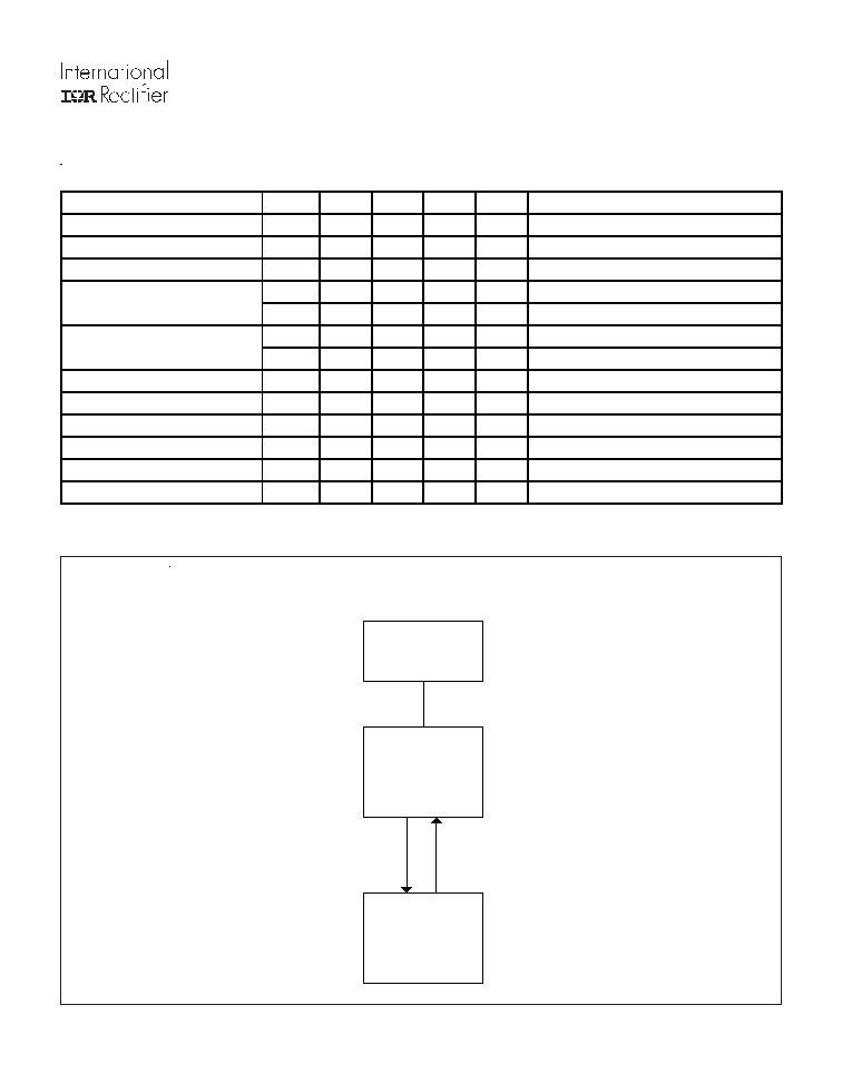
STATE AND TRANSITIONS DIAGRAM
POWER ON
Gate Inactive
UVLO MODE
VCC < VCCon
Gate Inactive
ICC max = 200uA
NORMAL
Gate Active
VCC > VCCon
and
ENABLE HIGH
VCC < VCCuvlo
or
ENABLE LOW
**
Guaranteed by Design
Gate Driver Section
Parameters
Symbol Min.
Typ.
Max.
Units
Gate Low Voltage
V
GLO
0.3
0.5
V
Gate High Voltage
V
GTH
9.5
10.7
12.5
V
Gate High Voltage
V
GTH
12.5
14.5
16.5
V
Rise Time
t
r1
30
ns
t
r2
180
ns
Fall Time
t
f1
10
ns
t
f2
30
ns
Turn on Propagation Delay
t
Don
60
80
ns
Turn off Propagation Delay
t
Doff
40
60
ns
Pull up Resistance
r
up
4
Pull down Resistance
r
down
0.7
Output Peak Current (source)
I
O source
2
A
Output Peak Current (sink)
I
O sink
7
A
IR1167A - V
CC
=12V-18V (internally clamped)
Remarks
I
GATE
= 200mA
I
GATE
= -200mA
IR1167B - V
CC
=12V-18V (internally clamped)
C
LOAD
= 1nF, V
CC
=12V
C
LOAD
= 1nF, V
CC
=12V
C
LOAD
= 10nF, V
CC
=12V
C
LOAD
= 10nF, V
CC
=12V
C
LOAD
= 10nF - GBD
C
LOAD
= 10nF - GBD
V
DS
to V
GATE
-100mV overdrive
V
DS
to V
GATE
-100mV overdrive
I
GATE
= 1A - GBD