 | –≠–ª–µ–∫—Ç—Ä–æ–Ω–Ω—ã–π –∫–æ–º–ø–æ–Ω–µ–Ω—Ç: IR21271S | –°–∫–∞—á–∞—Ç—å:  PDF PDF  ZIP ZIP |

Features
∑
Floating channel designed for bootstrap operation
Fully operational to +600V
Tolerant to negative transient voltage dV/dt immune
∑
Application- specific gate drive range:
Motor Drive: 12 to 20V (IR2127/IR2128)
Automotive: 9 to 20V (IR21271)
∑
Undervoltage lockout
∑
3.3V, 5V and 15V input logic compatible
∑
FAULT lead indicates shutdown has occured
∑
Output in phase with input (IR2127/IR21271)
∑
Output out of phase with input (IR2128)
CURRENT SENSING SINGLE CHANNEL DRIVER
V
OFFSET
600V max.
I
O
+/-
200 mA / 420 mA
V
OUT
12 - 20V 9 - 20V
(IR2127/IR2128) (IR21271)
V
CSth
250 mV or 1.8V
t
on/off
(typ.)
200 & 150 ns
Typical Connection
www.irf.com
1
Packages
IR2127/IR21271
IR2128
8-Lead PDIP
8-Lead SOIC
IR2127(S) / IR2128(S)
IR21271(S)
Data Sheet No. PD60143-N
Description
The IR2127/IR2128/IR21271(S) is a high voltage, high
speed power MOSFET and IGBT driver. Proprietary
HVIC and latch immune CMOS technologies enable
ruggedized monolithic construction. The logic input is
compatible with standard CMOS or LSTTL outputs,
down to 3.3V. The protection circuity detects over-cur-
rent in the driven power transistor and terminates the
gate drive voltage. An open drain FAULT signal is pro-
vided to indicate that an over-current shutdown has oc-
curred. The output driver features a high pulse current
buffer stage designed for minimum cross-conduction.
The floating channel can be used to drive an N-chan-
nel power MOSFET or IGBT in the high side or low
side configuration which operates up to 600 volts.
Product Summary
V
CC
V
B
CS
HO
V
S
COM
IN
FAULT
V
CC
IN
FAULT
V
CC
V
B
CS
HO
V
S
COM
IN
FAULT
V
CC
IN
FAULT
(Refer to Lead Assignments for correct pin
configuration). This/These diagram(s) show
electrical connections only. Please refer to
our Application Notes and DesignTips for
proper circuit board layout.

2
www.irf.com
IR2127(S) / IR21271(S) / IR2128(S)
Symbol
Definition
Min.
Max.
Units
V
B
High Side Floating Supply Voltage
-0.3
625
V
S
High Side Floating Offset Voltage
V
B
- 25
V
B
+ 0.3
V
HO
High Side Floating Output Voltage
V
S
- 0.3
V
B
+ 0.3
V
CC
Logic Supply Voltage
-0.3
25
V
V
IN
Logic Input Voltage
-0.3
V
CC
+ 0.3
V
FLT
FAULT Output Voltage
-0.3
V
CC
+ 0.3
V
CS
Current Sense Voltage
V
S
- 0.3
V
B
+ 0.3
dV
s
/dt
Allowable Offset Supply Voltage Transient
--
50
V/ns
P
D
Package Power Dissipation @ T
A
+25∞C
(8 Lead DIP)
--
1.0
(8 Lead SOIC)
--
0.625
Rth
JA
Thermal Resistance, Junction to Ambient
(8 Lead DIP)
--
125
(8 Lead SOIC)
--
200
T
J
Junction Temperature
--
150
T
S
Storage Temperature
-55
150
T
L
Lead Temperature (Soldering, 10 seconds)
--
300
Absolute Maximum Ratings
Absolute Maximum Ratings indicate sustained limits beyond which damage to the device may occur. All voltage param-
eters are absolute voltages referenced to COM. The Thermal Resistance and Power Dissipation ratings are measured
under board mounted and still air conditions.
Symbol
Definition
Min.
Max.
Units
V
B
High Side Floating Supply Voltage (IR2127/IR2128)
V
S
+ 12
V
S
+ 20
(IR21271)
V
S
+ 9
V
S
+ 20
V
S
High Side Floating Offset Voltage
Note 1
600
V
HO
High Side Floating Output Voltage
V
S
V
B
V
CC
Logic Supply Voltage
10
20
V
IN
Logic Input Voltage
0
V
CC
V
FLT
FAULT Output Voltage
0
V
CC
V
CS
Current Sense Signal Voltage
V
S
V
S
+ 5
T
A
Ambient Temperature
-40
125
∞C
Note 1: Logic operational for V
S
of -5 to +600V. Logic state held for V
S
of -5V to -V
BS
. (Please refer to the Design Tip
DT97-3 for more details).
Recommended Operating Conditions
The Input/Output logic timing diagram is shown in Figure 1. For proper operation the device should be used within the
recommended conditions. The V
S
offset rating is tested with all supplies biased at 15V differential.
∞C/W
W
∞C
V

www.irf.com
3
IR2127(S) / IR21271(S) / IR2128(S)
Symbol
Definition
Min.
Typ. Max. Units Test Conditions
V
IH
Logic "1" Input Voltage
(IR2127/IR21271)
Logic "0" Input Voltage
(IR2128)
V
IL
Logic "0" Input Voltage
(IR2127/IR21271)
Logic "1" Input Voltage
(IR2128)
V
CSTH+
CS Input Positive
(IR2127/IR2128)
180 250
320
mV
Going Threshold
(IR21271)
--
1.8
--
V
V
OH
High Level Output Voltage, V
BIAS
- V
O
--
--
100
I
O
= 0A
V
OL
Low Level Output Voltage, V
O
--
--
100
I
O
= 0A
I
LK
Offset Supply Leakage Current
--
--
50
V
B
= V
S
= 600V
I
QBS
Quiescent V
BS
Supply Current
--
200
400
I
QCC
Quiescent V
CC
Supply Current
--
60
120
I
IN+
Logic "1" Input Bias Current
--
7.0
15
V
IN
= 5V
I
IN-
Logic "0" Input Bias Current
--
--
1.0
V
IN
= 0V
I
CS+
"High" CS Bias Current
--
--
1.0
V
CS
= 3V
I
CS-
"High" CS Bias Current
--
--
1.0
V
CS
= 0V
V
BSUV+
V
BS
Supply Undervoltage
(IR2127/IR2128)
8.8
10.3
11.8
Positive Going Threshold
(IR21271)
6.3
7.2
8.2
V
BSUV-
V
BS
Supply Undervoltage
(IR2127/IR2128)
7.5
9.0
10.6
Negative Going Threshold
(IR21271)
6.0
6.8
7.7
I
O+
Output High Short Circuit Pulsed Current
200
250
--
V
O
= 0V, V
IN
= 5V
PW
10 µs
I
O-
Output Low Short Circuit Pulsed Current
420
500
--
V
O
= 15V, V
IN
= 0V
PW
10 µs
Ron, FLT
FAULT - Low on Resistance
--
125
--
Symbol
Definition
Min.
Typ. Max. Units Test Conditions
t
on
Turn-On Propagation Delay
--
200
250
V
S
= 0V
t
off
Turn-Off Propagation Delay
--
150
200
V
S
= 600V
t
r
Turn-On Rise Time
--
80
130
t
f
Turn-Off Fall Time
--
40
65
ns
t
bl
Start-Up Blanking Time
500
700
900
t
cs
CS Shutdown Propagation Delay
--
240
360
t
flt
CS to FAULT Pull-Up Propagation Delay
--
340
510
Dynamic Electrical Characteristics
V
BIAS
(V
CC
, V
BS
) = 15V, C
L
= 1000 pF and T
A
= 25∞C unless otherwise specified. The dynamic electrical characteristics
are measured using the test circuit shown in Figure 3.
Static Electrical Characteristics
V
BIAS
(V
CC
, V
BS
) = 15V and T
A
= 25∞C unless otherwise specified. The V
IN
, V
TH
and I
IN
parameters are referenced to
COM. The V
O
and I
O
parameters are referenced to V
S
.
3.0 -- --
-- -- 0.8 V
CC
= 10V to 20V
V
IN
= 0V or 5V
mV
µA
mA
V
V

4
www.irf.com
IR2127(S) / IR21271(S) / IR2128(S)
Functional Block Diagram IR2127/IR21271
DOWN
SHIFTER
PULSE
GEN
UV
DETECT
PULSE
FILTER
PULSE
GEN
BUFFER
HV
LEVEL
V
B
HO
V
S
CS
R
S
R
Q
V
CC
IN
UP
SHIFTERS
COM
FAULT
-
+
PULSE
FILTER
V
B
DELAY
S
Q
R
Q
R
S
SHIFT
Functional Block Diagram IR2128
D O W N
SHIFTER
PULSE
G E N
UV
DETECT
PULSE
FILTER
PULSE
G E N
BUFFER
HV
LEVEL
V
B
H O
V
S
C S
R
S
R
Q
V
CC
IN
U P
SHIFTERS
C O M
FAULT
-
+
PULSE
FILTER
V
B
DELAY
S
Q
R
Q
R
S
SHIFT
5V
www.irf.com
5
IR2127(S) / IR21271(S) / IR2128(S)
Lead Definitions
Symbol
Description
V
CC
Logic and gate drive supply
IN
Logic input for gate driver output (HO), in phase with HO (IR2127/IR21271)
out of phase with HO (IR2128)
Indicates over-current shutdown has occurred, negative logic
COM
Logic ground
V
B
High side floating supply
HO
High side gate drive output
V
S
High side floating supply return
CS
Current sense input to current sense comparator
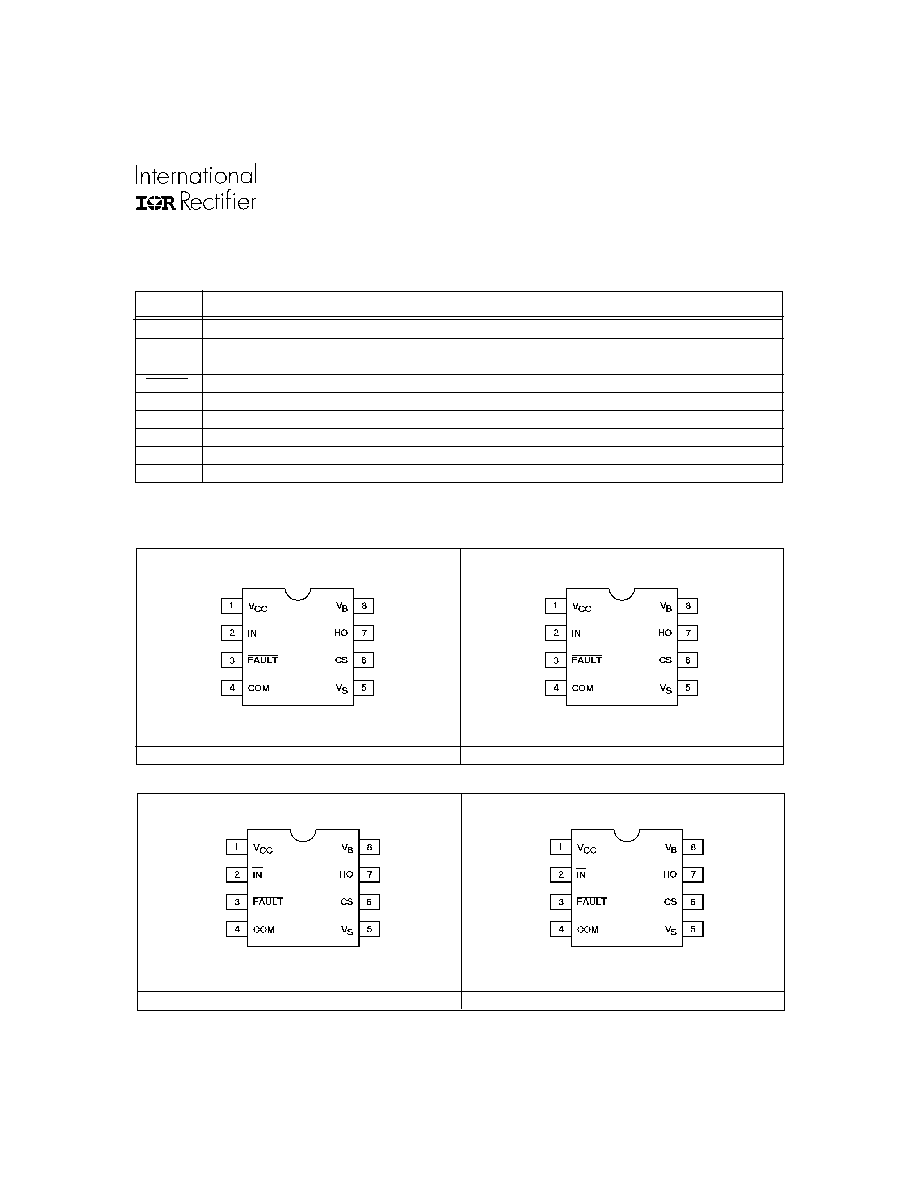
Lead Assignments
8 Lead PDIP
8 Lead SOIC
IR2127/IR21271
IR2127S/IR21271S
FAULT
8 Lead PDIP
8 Lead SOIC
IR2128
IR2128S