IRF7503
PD - 9.1266G
Fifth Generation HEXFETs from International Rectifier
utilize advanced processing techniques to achieve
extremely low on-resistance per silicon area. This benefit,
combined with the fast switching speed and ruggedized
device design that HEXFET Power MOSFETs are well
known for, provides the designer with an extremely efficient
and reliable device for use in a wide variety of applications.
The new Micro8 package, with half the footprint area of the
standard SO-8, provides the smallest footprint available in
an SOIC outline. This makes the Micro8 an ideal device for
applications where printed circuit board space is at a
premium. The low profile (<1.1mm) of the Micro8 will allow
it to fit easily into extremely thin application environments
such as portable electronics and PCMCIA cards.
l
Generation V Technology
l
Ultra Low On-Resistance
l
Dual N-Channel MOSFET
l
Very Small SOIC Package
l
Low Profile (<1.1mm)
l
Available in Tape & Reel
l
Fast Switching
V
DSS
= 30V
R
DS(on)
= 0.135
HEXFET
�
Power MOSFET
Description
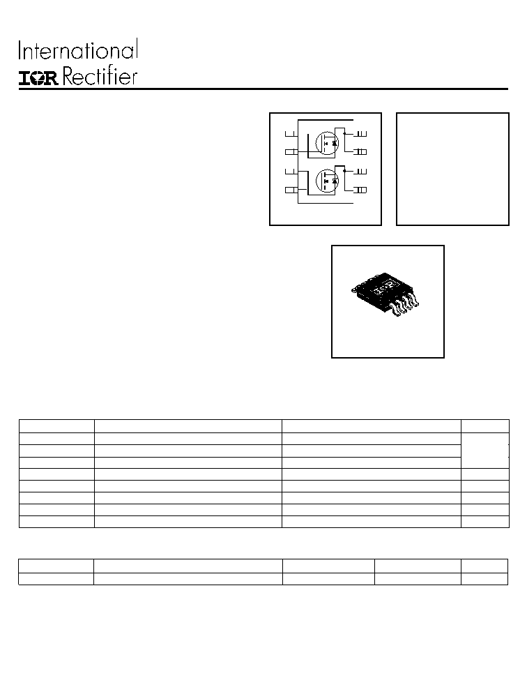
M icro8
D 1
D 1
D 2
D 2
G 1
S 2
G 2
S 1
T o p V iew
8
1
2
3
4
5
6
7
8/25/97
Thermal Resistance
Parameter
Max.
Units
I
D
@ T
A
= 25�C
Continuous Drain Current, V
GS
@ 10V
2.4
I
D
@ T
A
= 70�C
Continuous Drain Current, V
GS
@ 10V
1.9
A
I
DM
Pulsed Drain Current
14
P
D
@T
A
= 25�C
Power Dissipation
1.25
W
Linear Derating Factor
10
mW/�C
V
GS
Gate-to-Source Voltage
� 20
V
dv/dt
Peak Diode Recovery dv/dt
5.0
V/ns
T
J,
T
STG
Junction and Storage Temperature Range
-55 to + 150
�C
Absolute Maximum Ratings
All Micro8 Data Sheets reflect improved Thermal Resistance, Power and Current -Handling Ratings- effective
only for product marked with Date Code 505 or later .
Parameter
Typ.
Max.
Units
R
JA
Maximum Junction-to-Ambient
���
100
�C/W
IRF7503
Parameter
Min. Typ. Max. Units
Conditions
V
(BR)DSS
Drain-to-Source Breakdown Voltage
30
���
���
V
V
GS
= 0V, I
D
= 250�A
V
(BR)DSS
/
T
J
Breakdown Voltage Temp. Coefficient
��� 0.059 ���
V/�C
Reference to 25�C, I
D
= 1mA
���
��� 0.135
V
GS
= 10V, I
D
= 1.7A
���
��� 0.222
V
GS
= 4.5V, I
D
= 0.85A
V
GS(th)
Gate Threshold Voltage
1.0
���
���
V
V
DS
= V
GS
, I
D
= 250�A
g
fs
Forward Transconductance
1.9
���
���
S
V
DS
= 10V, I
D
= 0.85A
���
���
1.0
V
DS
= 24V, V
GS
= 0V
���
���
25
V
DS
= 24V, V
GS
= 0V, T
J
= 125�C
Gate-to-Source Forward Leakage
���
���
-100
V
GS
= -20V
Gate-to-Source Reverse Leakage
���
���
100
V
GS
= 20V
Q
g
Total Gate Charge
���
7.8
12
I
D
= 1.7A
Q
gs
Gate-to-Source Charge
���
1.2
1.8
nC
V
DS
= 24V
Q
gd
Gate-to-Drain ("Miller") Charge
���
2.5
3.8
V
GS
= 10V, See Fig. 6 and 9
t
d(on)
Turn-On Delay Time
���
4.7
���
V
DD
= 15V
t
r
Rise Time
���
10
���
I
D
= 1.7A
t
d(off)
Turn-Off Delay Time
���
12
���
R
G
= 6.1
t
f
Fall Time
���
5.3
���
R
D
= 8.7
,
See Fig. 10
C
iss
Input Capacitance
���
210
���
V
GS
= 0V
C
oss
Output Capacitance
���
80
���
pF
V
DS
= 25V
C
rss
Reverse Transfer Capacitance
���
32
���
= 1.0MHz, See Fig. 5
�A
nA
ns
I
GSS
I
DSS
Drain-to-Source Leakage Current
R
DS(on)
Static Drain-to-Source On-Resistance
Electrical Characteristics @ T
J
= 25�C (unless otherwise specified)
Notes:
Repetitive rating; pulse width limited by
max. junction temperature. ( See fig. 11 )
Pulse width
300�s; duty cycle
2%.
I
SD
1.7A, di/dt
120A/�s, V
DD
V
(BR)DSS
,
T
J
150�C
Parameter
Min. Typ. Max. Units
Conditions
I
S
Continuous Source Current
MOSFET symbol
(Body Diode)
showing the
I
SM
Pulsed Source Current
integral reverse
(Body Diode)
p-n junction diode.
V
SD
Diode Forward Voltage
���
���
1.2
V
T
J
= 25�C, I
S
= 1.7A, V
GS
= 0V
t
rr
Reverse Recovery Time
���
40
60
ns
T
J
= 25�C, I
F
= 1.7A
Q
rr
Reverse RecoveryCharge
���
48
72
nC
di/dt = 100A/�s
Source-Drain Ratings and Characteristics
A
���
���
14
���
���
1.25
S
D
G
Surface mounted on FR-4 board, t
10sec.
IRF7503
Fig 4. Normalized On-Resistance
Vs. Temperature
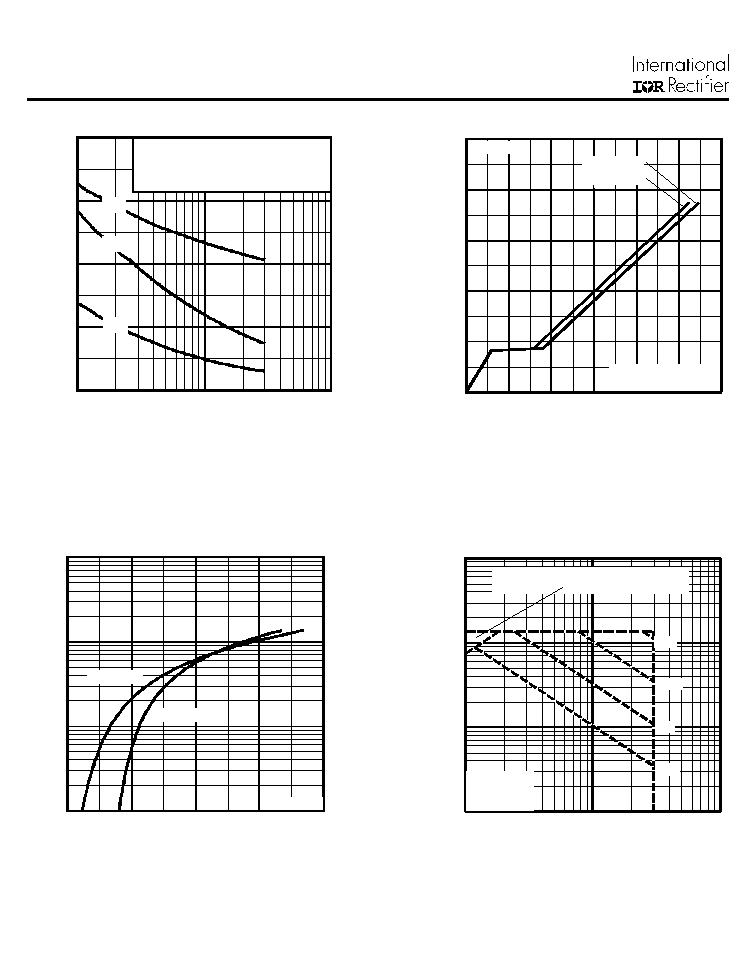
Fig 1. Typical Output Characteristics
Fig 2. Typical Output Characteristics
Fig 3. Typical Transfer Characteristics
0 . 1
1
1 0
1 0 0
0 . 1
1
1 0
20 �s P U LSE W I DTH
T = 25 �C
A
J
D S
V , D ra in-to-S ou rce V o lta ge (V )
3.0 V
VGS
TOP 15V
10V
7.0V
5.5V
4.5V
4.0V
3.5V
BOTT OM 3.0V
DI
,
D
r
ai
n-
t
o
-
S
our
c
e
C
u
r
r
ent
(
A
)
0 . 1
1
1 0
1 0 0
0 . 1
1
1 0
A
D S
V , D rain-to -S ou rce Vo lta ge (V)
D
I
,
D
r
ai
n-
t
o
-
S
our
c
e
C
u
r
r
ent
(
A
)
20 �s P U LSE W I DTH
T = 15 0�C
J
3. 0V
VGS
TOP 15V
10V
7.0V
5.5V
4.5V
4.0V
3.5V
BOTT OM 3.0V
0 . 0
0 . 5
1 . 0
1 . 5
2 . 0
- 6 0
- 4 0
- 2 0
0
2 0
4 0
6 0
8 0
1 0 0
1 2 0
1 4 0
1 6 0
J
T , Ju nctio n T emp eratu re (�C)
R
,
D
r
a
i
n
-
to
-
S
o
u
r
c
e
O
n
R
e
s
i
s
t
a
n
c
e
D
S
(
on)
(
N
o
r
m
a
l
i
z
ed)
V = 10 V
G S
A
I = 1. 7A
D
0 . 1
1
1 0
1 0 0
3 . 0
3 . 5
4 . 0
4 . 5
5 . 0
5 . 5
6 . 0
T = 2 5 � C
T = 1 5 0 �C
J
J
G S
V , Ga te -to -S o u rce V o l ta g e (V )
D
I
, D
r
a
i
n
-
to
-
S
o
u
r
c
e
C
u
r
r
e
n
t
(
A
)
A
V = 1 0V
2 0 � s P U L S E W ID T H
D S
IRF7503
Fig 7. Typical Source-Drain Diode
Forward Voltage
Fig 5. Typical Capacitance Vs.
Drain-to-Source Voltage
Fig 8. Maximum Safe Operating Area
Fig 6. Typical Gate Charge Vs.
Gate-to-Source Voltage
0
1 0 0
2 0 0
3 0 0
4 0 0
1
1 0
1 0 0
C
,
C
a
pac
i
t
anc
e (
p
F
)
D S
V , Drai n-to -So urce V oltag e (V)
A
V = 0 V, f = 1M H z
C = C + C , C SH O RTE D
C = C
C = C + C
G S
is s gs gd ds
rs s gd
o ss ds g d
C
is s
C
o s s
C
rs s
0
4
8
1 2
1 6
2 0
0
2
4
6
8
1 0
1 2
Q , To tal Ga te Ch arg e (nC )
G
V
,
G
a
te
-
t
o
-
S
o
u
r
c
e
V
o
l
t
a
g
e
(
V
)
GS
A
FO R TES T C IR CU I T
SEE FIG U R E 9
V = 24 V
V = 15 V
I = 1 .7 A
D S
D S
D
0 . 1
1
1 0
1 0 0
0 . 4
0 . 8
1 . 2
1 . 6
2 . 0
T = 2 5�C
T = 150 �C
J
J
V = 0 V
G S
V , S o urce-to -Drain Vo lta ge (V )
I
, R
e
v
e
r
s
e
D
r
a
i
n
C
u
r
r
e
n
t
(
A
)
S D
SD
A
0 . 1
1
1 0
1 0 0
1
1 0
1 0 0
V , Dra in -to-So urce Vo ltag e (V)
D S
I
,
D
r
ai
n C
u
r
r
en
t
(
A
)
OPE R ATIO N IN TH IS A RE A LI MI TE D
BY R
D
D S(o n)
T = 25 �C
T = 15 0�C
S ing le Pulse
1 ms
10m s
A
A
J
100� s
1 0�s
IRF7503
Fig 10a. Switching Time Test Circuit
+
-
V
DS
10V
Pulse Width
1
�s
Duty Factor
0.1 %
R
D
V
GS
V
DD
R
G
D.U.T.
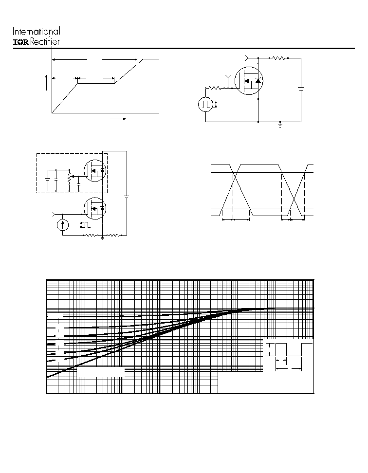
Fig 11. Maximum Effective Transient Thermal Impedance, Junction-to-Ambient
10V
Q
G
Q
GS
Q
GD
V
G
Charge
Fig 9a. Basic Gate Charge Waveform
D.U.T.
V
DS
I
D
I
G
3mA
V
GS
.3
�
F
50K
.2
�
F
12V
Current Regulator
Same Type as D.U.T.
Current Sampling Resistors
+
-
V
DS
90%
10%
V
GS
t
d(on)
t
r
t
d(off)
t
f
Fig 9b. Gate Charge Test Circuit
Fig 10b. Switching Time Waveforms
0.1
1
10
100
1000
0.00001
0.0001
0.001
0.01
0.1
1
10
100
Notes:
1. Duty factor D =
t / t
2. Peak T
= P
x Z
+ T
1
2
J
DM
thJA
A
P
t
t
DM
1
2
t , Rectangular Pulse Duration (sec)
Thermal Response
(Z )
1
thJA
0.01
0.02
0.05
0.10
0.20
D = 0.50
SINGLE PULSE
(THERMAL RESPONSE)