 | –≠–ª–µ–∫—Ç—Ä–æ–Ω–Ω—ã–π –∫–æ–º–ø–æ–Ω–µ–Ω—Ç: IRF7509 | –°–∫–∞—á–∞—Ç—å:  PDF PDF  ZIP ZIP |

IRF7509
PD - 91270J
q
Generation V Technology
q
Ultra Low On-Resistance
q
Dual N and P Channel MOSFET
q
Very Small SOIC Package
q
Low Profile (<1.1mm)
q
Available in Tape & Reel
q
Fast Switching
HEXFET
Æ
Power MOSFET
N-Ch
P-Ch
V
DSS
30V
-30V
R
DS(on)
0.11
0.20
12/1/98
M icro 8
Fifth Generation HEXFETs from International Rectifier utilize advanced
processing techniques to achieve extremely low on-resistance per silicon
area. This benefit, combined with the fast switching speed and ruggedized
device design that HEXFET Power MOSFETs are well known for, provides the
designer with an extremely efficient and reliable device for use in a wide variety
of applications.
The new Micro8 package, with half the footprint area of the standard SO-8,
provides the smallest footprint available in an SOIC outline. This makes the
Micro8 an ideal device for applications where printed circuit board space is at
a premium. The low profile (<1.1mm) of the Micro8 will allow it to fit easily into
extremely thin application environments such as portable electronics and
PCMCIA cards.
Description
D 1
D 1
D 2
D 2
G 1
S 2
G 2
S 1
T op V ie w
8
1
2
3
4
5
6
7
N-C HANNE L M O S F E T
P -C HANNE L M O S F E T
www.irf.com
1
Parameter
Max.
Units
N-Channel P-Channel
V
DS
Drain-Source Voltage 30 -30 V
I
D
@ T
A
= 25∞C
Continuous Drain Current, V
GS
2.7 -2.0
I
D
@ T
A
= 70∞C
Continuous Drain Current, V
GS
2.1 -1.6
A
I
DM
Pulsed Drain Current
21 -16
P
D
@T
A
= 25∞C
Maximum Power Dissipation
1.25
W
P
D
@T
A
= 70∞C
Maximum Power Dissipation
0.8
W
Linear Derating Factor 10 mW/∞C
V
GS
Gate-to-Source Voltage
± 20 V
V
GSM
Gate-to-Source Voltage Single Pulse tp<10µS 30 V
dv/dt
Peak Diode Recovery dv/dt
5.0
V/ns
T
J
, T
STG
Junction and Storage Temperature Range
-55 to + 150
∞C
Soldering Temperature, for 10 seconds 240 (1.6mm from case)
Thermal Resistance
Parameter
Max. Units
R
JA
Maximum Junction-to-Ambient
100 ∞C/W
Absolute Maximum Ratings

IRF7509
2
www.irf.com
Parameter
Min. Typ. Max. Units
Conditions
N-Ch
30
--
--
V
GS
= 0V, I
D
= 250µA
P-Ch -30
--
--
V
GS
= 0V, I
D
= -250µA
N-Ch
-- 0.059
--
Reference to 25∞C, I
D
= 1mA
P-Ch
-- -0.039 --
Reference to 25∞C, I
D
= -1mA
--
0.09 0.110
V
GS
= 10V, I
D
= 1.7A
--
0.14 0.175
V
GS
= 4.5V, I
D
= 0.85A
--
0.17 0.20
V
GS
= -10V, I
D
=-1.2A
--
0.30 0.40
V
GS
= -4.5V, I
D
=-0.6A
N-Ch 1.0
--
--
V
DS
= V
GS
, I
D
= 250µA
P-Ch -1.0
--
--
V
DS
= V
GS
, I
D
= -250µA
N-Ch 1.9
--
--
V
DS
= 10V, I
D
= 0.85A
P-Ch 0.92
--
--
V
DS
= -10V, I
D
= -0.6A
N-Ch
--
--
1.0
V
DS
= 24 V, V
GS
= 0V
P-Ch
--
--
-1.0
V
DS
= -24V, V
GS
= 0V
N-Ch
--
--
25
V
DS
= 24 V, V
GS
= 0V, T
J
= 125∞C
P-Ch
--
--
-25
V
DS
= -24V, V
GS
= 0V, T
J
= 125∞C
I
GSS
Gate-to-Source Forward Leakage
N-P
≠≠
--
±100
V
GS
= ± 20V
N-Ch
≠≠
7.8
12
P-Ch
--
7.5
11
N-Ch
≠≠
1.2
1.8
P-Ch
--
1.3
1.9
N-Ch
≠≠
2.5
3.8
P-Ch
--
2.5
3.7
N-Ch
--
4.7
--
P-Ch
--
9.7
--
N-Ch
--
10
--
P-Ch
--
12
--
N-Ch
--
12
--
P-Ch
--
19
--
N-Ch
--
5.3
--
P-Ch
--
9.3
--
N-Ch
--
210
--
P-Ch
--
180
--
N-Ch
--
80
--
pF
P-Ch
--
87
--
N-Ch
--
32
--
P-Ch
--
42
--
V
(BR)DSS
Drain-to-Source Breakdown Voltage
V
(BR)DSS
/
T
J
Breakdown Voltage Temp. Coefficient
R
DS(ON)
Static Drain-to-Source On-Resistance
V
GS(th)
Gate Threshold Voltage
g
fs
Forward Transconductance
I
DSS
Drain-to-Source Leakage Current
Q
g
Total Gate Charge
Q
gs
Gate-to-Source Charge
Q
gd
Gate-to-Drain ("Miller") Charge
t
d(on)
Turn-On Delay Time
t
r
Rise Time
t
d(off)
Turn-Off Delay Time
t
f
Fall Time
C
iss
Input Capacitance
C
oss
Output Capacitance
C
rss
Reverse Transfer Capacitance
Repetitive rating; pulse width limited by
max. junction temperature. ( See fig. 21 )
Notes:
N-Channel I
SD
1.7A, di/dt
120A/µs, V
DD
V
(BR)DSS
, T
J
150∞C
P-Channel I
SD
-1.2A, di/dt
160A/µs, V
DD
V
(BR)DSS
, T
J
150∞C
Parameter
Min. Typ. Max. Units
Conditions
N-Ch
--
--
1.25
P-Ch
--
--
-1.25
N-Ch
--
--
21
P-Ch
--
--
-16
N-Ch
--
--
1.2
T
J
= 25∞C, I
S
= 1.7A, V
GS
= 0V
P-Ch
--
--
-1.2
T
J
= 25∞C, I
S
= -1.8A, V
GS
= 0V
N-Ch
--
40
60
P-Ch
--
30
45
N-Ch
--
48
72
P-Ch
--
37
55
Electrical Characteristics @ T
J
= 25∞C (unless otherwise specified)
Source-Drain Ratings and Characteristics
V
V/∞C
V
S
µA
nC
ns
N-Channel
I
D
= 1.7A, V
DS
= 24V, V
GS
= 10V
P-Channel
I
D
= -1.2A, V
DS
= -24V, V
GS
= -10V
N-Channel
V
DD
= 15V, I
D
= 1.7A, R
G
= 6.1
,
R
D
= 8.7
P-Channel
V
DD
= -15V, I
D
= -1.2A, R
G
= 6.2
,
R
D
= 12
N-Channel
V
GS
= 0V, V
DS
= 25V, = 1.0MHz
P-Channel
V
GS
= 0V, V
DS
= -25V, = 1.0MHz
N-Ch
P-Ch
I
S
Continuous Source Current (Body Diode)
I
SM
Pulsed Source Current (Body Diode)
V
SD
Diode Forward Voltage
t
rr
Reverse Recovery Time
Q
rr
Reverse Recovery Charge
A
V
ns
nC
N-Channel
T
J
= 25∞C, I
F
= 1.7A, di/dt = 100A/µs
P-Channel
T
J
= 25∞C, I
F
= -1.2A, di/dt = -100A/µs
Pulse width
300µs; duty cycle
2%.
Surface mounted on FR-4 board, t
10sec.
IRF7509
www.irf.com
3
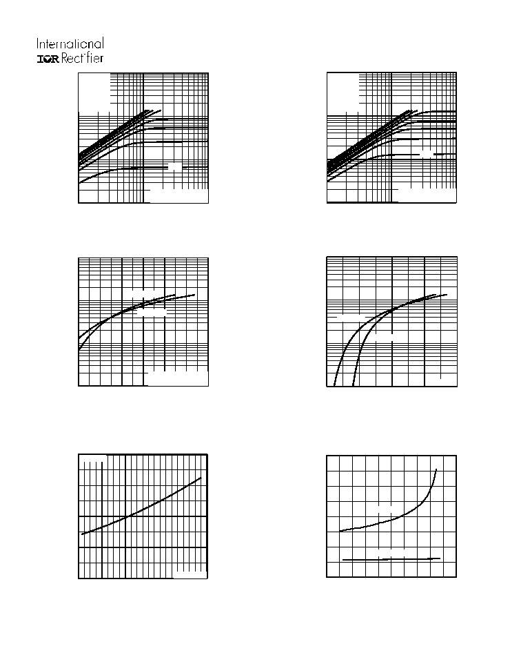
Fig 1. Typical Output Characteristics
Fig 3. Typical Transfer Characteristics
Fig 2. Typical Output Characteristics
0.1
1
1 0
1 0 0
0.1
1
1 0
20µ s P U LS E W ID TH
T = 25∞C
A
J
D S
V , D ra in-to-S o urc e V o ltage (V )
3.0V
VGS
TOP 15V
10V
7.0V
5.5V
4.5V
4.0V
3.5V
BOTTOM 3.0V
DI
,
Dr
ai
n
-
t
o
-
S
o
u
r
c
e C
u
r
r
ent
(
A
)
0.1
1
1 0
1 0 0
0.1
1
1 0
A
D S
V , D ra in-to-S o urce V olta ge (V )
DI ,
D
r
a
i
n
-
t
o
-
S
o
u
r
c
e
C
u
r
r
e
n
t (
A
)
20µ s P U LS E W ID TH
T = 150∞C
J
3.0V
VGS
TOP 15V
10V
7.0V
5.5V
4.5V
4.0V
3.5V
BOTTOM 3.0V
0.1
1
1 0
1 0 0
3.0
3.5
4.0
4.5
5.0
5.5
6.0
T = 2 5 ∞C
T = 1 5 0 ∞C
J
J
G S
V , G a te -to -S o u rc e V o lta g e (V )
D
I
,
D
r
ai
n-
t
o
-
S
o
u
r
c
e C
u
r
r
ent
(
A
)
A
V = 1 0 V
2 0 µ s P U L S E W ID T H
D S
Fig 4. Typical Source-Drain Diode
Forward Voltage
0.1
1
1 0
1 0 0
0.4
0.8
1.2
1.6
2.0
T = 25∞ C
T = 150∞C
J
J
V = 0V
G S
V , S ource-to -D rain V o lta ge (V )
I
,
R
e
v
e
rs
e
D
r
a
i
n
C
u
rre
n
t
(A
)
S D
SD
A
Fig 5. Normalized On-Resistance
Vs. Temperature
0 . 0
0 . 5
1 . 0
1 . 5
2 . 0
- 6 0
- 4 0
- 2 0
0
2 0
4 0
6 0
8 0
1 0 0
1 2 0
1 4 0
1 6 0
J
T , J u n c tio n T e m pe ra tu re (∞C )
R
,
D
r
a
i
n
-
to
-
S
o
u
r
c
e
O
n
R
e
s
i
s
t
a
n
c
e
D
S
(
on)
(N
o
r
m
a
li
z
e
d
)
V = 1 0 V
G S
A
I = 1 .7A
D
Fig 6. Typical On-Resistance Vs. Drain
Current
0
2
4
6
8
10
0.060
0.100
0.140
0.180
0.220
R , Drain-to-Source On Resistance
I , Drain Current (A)
D
DS (on)
VGS = 10V
VGS = 4.5V
N - Channel
IRF7509
4
www.irf.com
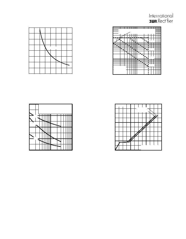
Fig 8. Maximum Safe Operating Area
Fig 9. Typical Capacitance Vs.
Drain-to-Source Voltage
Fig 10. Typical Gate Charge Vs.
Gate-to-Source Voltage
0
100
200
300
400
1
10
100
C
,
C
a
pa
c
i
t
a
n
c
e (
p
F
)
D S
V , D rain-to-S ourc e V oltage (V )
A
V = 0 V , f = 1 M H z
C = C + C , C S H O R T E D
C = C
C = C + C
GS
iss gs gd ds
rss gd
oss ds gd
C
is s
C
o s s
C
rs s
0
4
8
12
16
20
0
2
4
6
8
10
12
Q , Tota l G ate C harg e (n C )
G
V
,
G
a
t
e
-
t
o-
S
our
c
e
V
o
l
t
ag
e (
V
)
GS
A
FO R TE S T C IR C U IT
S E E FIG U R E 9
V = 24V
V = 15V
I = 1.7A
D S
D S
D
Fig 7. Typical On-Resistance Vs. Gate
Voltage
0
4
8
12
16
0.060
0.080
0.100
0.120
0.140
R , Drain-to-Source On Resistance
V , Gate-to-Source Voltage (V)
GS
DS (on)
ID = 2.7A
N - Channel
0.1
1
10
100
1
10
100
OPERATION IN THIS AREA LIMITED
BY R
DS(on)
Single Pulse
T
T
= 150 C
= 25 C
∞
∞
J
C
V , Drain-to-Source Voltage (V)
I , Drain Current (A)
I , Drain Current (A)
DS
D
10us
100us
1ms
10ms

IRF7509
www.irf.com
5
Fig 11. Typical Output Characteristics
Fig 13. Typical Transfer Characteristics
Fig 12. Typical Output Characteristics
0.1
1
1 0
0.1
1
1 0
D
D S
20µ s P U LS E W ID TH
T = 25 ∞C
A
-
I
, D
r
a
i
n
-
to
-
S
o
u
r
c
e
C
u
r
r
e
n
t
(
A
)
-V , D ra in-to-S o urc e V o lta ge (V )
J
-3.0 V
VGS
TOP - 15V
- 10V
- 7.0V
- 5.5V
- 4.5V
- 4.0V
- 3.5V
BOTTOM - 3.0V
0.1
1
1 0
0.1
1
1 0
D
D S
A
-
I
,
D
r
ai
n-
t
o
-
S
ou
r
c
e
C
u
r
r
e
n
t
(
A
)
-V , D ra in-to-S ource V o ltage (V )
-3.0V
VGS
TOP - 15V
- 10V
- 7.0V
- 5.5V
- 4.5V
- 4.0V
- 3.5V
BOTTOM - 3.0V
20µs P U LS E W ID TH
T = 150∞C
J
0.1
1
1 0
3.0
4.0
5.0
6.0
7.0
T = 2 5∞C
T = 1 5 0 ∞C
J
J
G S
D
A
-
I
, D
r
a
i
n
-
to
-
S
o
u
r
c
e
C
u
r
r
e
n
t (
A
)
-V , G a te -to -S ou rce V olta ge (V )
V = -1 0 V
2 0 µ s P U L S E W ID T H
D S
Fig 14. Typical Source-Drain Diode
Forward Voltage
0.1
1
10
0.4
0.6
0.8
1.0
1.2
1.4
T = 25∞C
T = 1 5 0 ∞C
J
J
V = 0 V
G S
S D
SD
A
-
I
,
R
e
v
e
r
s
e D
r
a
i
n C
u
r
r
ent
(
A
)
-V , S o urc e-to -D rain V o ltage (V )
Fig 15. Normalized On-Resistance
Vs. Temperature
0 . 0
0 . 5
1 . 0
1 . 5
2 . 0
- 6 0
- 4 0
- 2 0
0
2 0
4 0
6 0
8 0
1 0 0 1 2 0
1 4 0 1 6 0
J
T , J u nc tion T e m pe ratu re (∞C )
R
,
D
r
a
i
n
-
to
-
S
o
u
r
c
e
O
n
R
e
s
i
s
t
a
n
c
e
D
S
(
on)
(
N
or
m
a
l
i
z
e
d)
A
V = -1 0 V
G S
I = -1 .2 A
D
Fig 16. Typical On-Resistance Vs. Drain
Current
R
DS(on)
, Drain-to-Source On Resistance
( )
0.0
0.5
1.0
1.5
0
1
2
3
4
A
VGS = -10V
VGS = -4.5V
,
-I , Drain Current (A)
P - Channel