 | ÐлекÑÑоннÑй компоненÑ: IRF7807V | СкаÑаÑÑ:  PDF PDF  ZIP ZIP |
Äîêóìåíòàöèÿ è îïèñàíèÿ www.docs.chipfind.ru
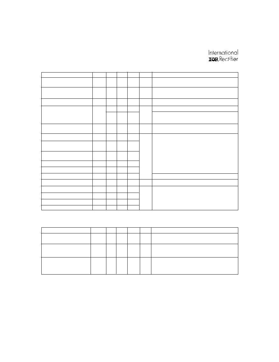
Parameter
Symbol
IRF7807 V
Units
Drain-Source Voltage
V
DS
30
V
Gate-Source Voltage
V
GS
±20
Continuous Drain or Source
T
A
= 25°C
I
D
8.3
Current (V
GS
4.5V)
T
A
= 70°C
6.6
A
Pulsed Drain Current
I
DM
66
Power Dissipation
T
A
= 25°C
P
D
2.5
W
T
A
= 70°C
1.6
Junction & Storage Temperature Range
T
J
,
T
STG
55 to 150
°C
Continuous Source Current (Body Diode)
I
S
2.5
A
Pulsed Source Current
I
SM
66
Absolute Maximum Ratings
Parameter
Max.
Units
Maximum Junction-to-Ambient
R
JA
50
°C/W
Maximum Junction-to-Lead
R
JL
20
°C/W
Thermal Resistance
PD-94108
IRF7807V
3/1/01
IRF7807V
R
DS
(on)
17m
Q
G
9.5nC
Q
sw
3.4nC
Q
oss
12nC
DEVICE CHARACTERISTICS
· N Channel Application Specific MOSFET
· Ideal for Mobile DC-DC Converters
· Low Conduction Losses
· Low Switching Losses
Description
This new device employs advanced HEXFET Power
MOSFET technology to achieve an unprecedented
balance of on-resistance and gate charge. The
reduction of conduction and switching losses makes
it ideal for high efficiency DC-DC Converters that
power the latest generation of mobile microprocessors.
A pair of IRF7807V devices provides the best cost/
performance solution for system voltages, such as
3.3V and 5V.
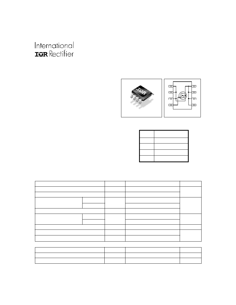
T o p V ie w
8
1
2
3
4
5
6
7
D
D
D
D
G
S
A
S
S
SO-8
IRF7807V
2
www.irf.com
Parameter
Min
Typ
Max
Units
Conditions
Diode Forward
V
SD
1.2
V
I
S
= 7.0A
, V
GS
= 0V
Voltage*
Reverse Recovery
Q
rr
64
nC
di/dt
~
700A/µs
V
DS
= 16V, V
GS
= 0V, I
S
= 7.0A
Reverse Recovery
Q
rr(s)
41
nC
di/dt = 700A/µs
Charge (with Parallel
(with 10BQ040)
Schottky)
V
DS
= 16V, V
GS
= 0V, I
S
= 7.0A
Parameter
Min
Typ
Max
Units
Conditions
Drain-to-Source
BV
DSS
30
V
V
GS
= 0V, I
D
= 250µA
Breakdown Voltage
Static Drain-Source
R
DS(on)
17
25
m
V
GS
= 4.5V, I
D
= 7.0A
on Resistance
Gate Threshold Voltage
V
GS(th)
1.0
V
V
DS
= V
GS
,I
D
= 250µA
Drain-Source Leakage
I
DSS
20
V
DS
= 24V, V
GS
= 0
Current*
100
µA
V
DS
= 24V, V
GS
= 0,
Tj = 100°C
Gate-Source Leakage
I
GSS
±100
nA
V
GS
= ±20V
Current*
Total Gate Charge*
Q
G
9.5
14
V
GS
=5V, I
D
=7.0A
Pre-Vth
Q
GS1
2.3
Gate-Source Charge
V
DS
= 16V
Post-Vth
Q
GS2
1.0
nC
Gate-Source Charge
Gate to Drain Charge
Q
GD
2.4
Switch Chg(Q
gs2
+ Q
gd
)
Q
sw
3.4
5.2
Output Charge*
Q
oss
12
16.8
V
DS
= 16V, V
GS
= 0
Gate Resistance
R
G
2.0
Turn-on Delay Time
t
d (on)
6.3
V
DD
= 16V, I
D
= 7.0A
Rise Time
t
r
1.2
ns V
GS
= 5V, R
G
=
2
Turn-off Delay Time
t
d
(off)
11
Resistive Load
Fall Time
t
f
2.2
Electrical Characteristics
Source-Drain Rating & Characteristics
Current
Charge
Notes:
Repetitive rating; pulse width limited by max. junction temperature.
Pulse width
400 µs; duty cycle
2%.
When mounted on 1 inch square copper board
Typ = measured - Q
oss
Typical values of R
DS
(on) measured at V
GS
= 4.5V, Q
G
, Q
SW
and Q
OSS
measured at V
GS
= 5.0V, I
F
= 7.0A.
* Device are 100% tested to these parameters.
IRF7807V
www.irf.com
3
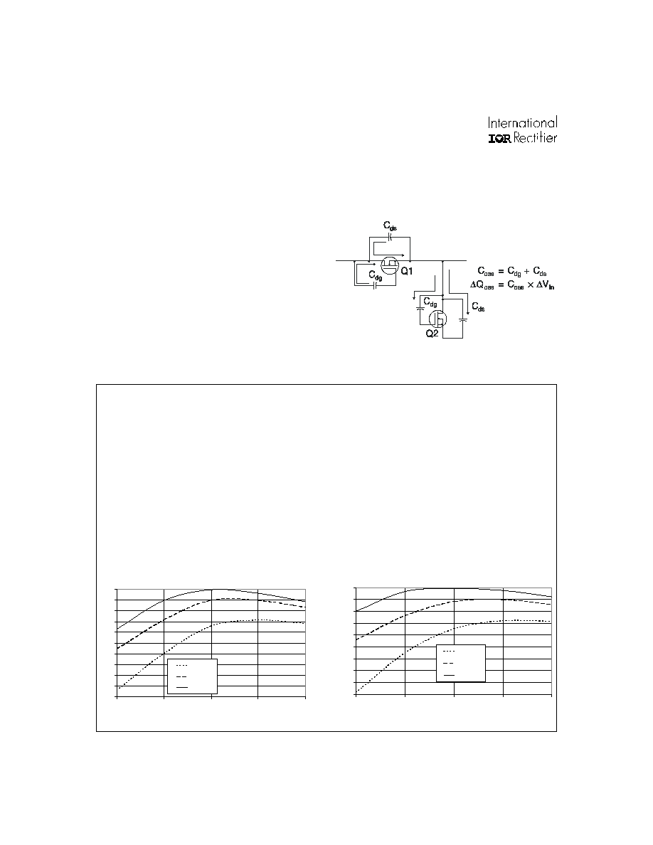
Control FET
Special attention has been given to the power losses
in the switching elements of the circuit - Q1 and Q2.
Power losses in the high side switch Q1, also called
the Control FET, are impacted by the R
ds(on)
of the
MOSFET, but these conduction losses are only about
one half of the total losses.
Power losses in the control switch Q1 are given
by;
P
loss
= P
conduction
+ P
switching
+ P
drive
+ P
output
This can be expanded and approximated by;
P
loss
=
I
rms
2
×
R
ds(on )
(
)
+
I
×
Q
gd
i
g
×
V
in
×
f
+
I
×
Q
gs 2
i
g
×
V
in
×
f
+
Q
g
×
V
g
×
f
(
)
+
Q
oss
2
×
V
in
×
f
This simplified loss equation includes the terms Q
gs2
and Q
oss
which are new to Power MOSFET data sheets.
Q
gs2
is a sub element of traditional gate-source
charge that is included in all MOSFET data sheets.
The importance of splitting this gate-source charge
into two sub elements, Q
gs1
and Q
gs2
, can be seen from
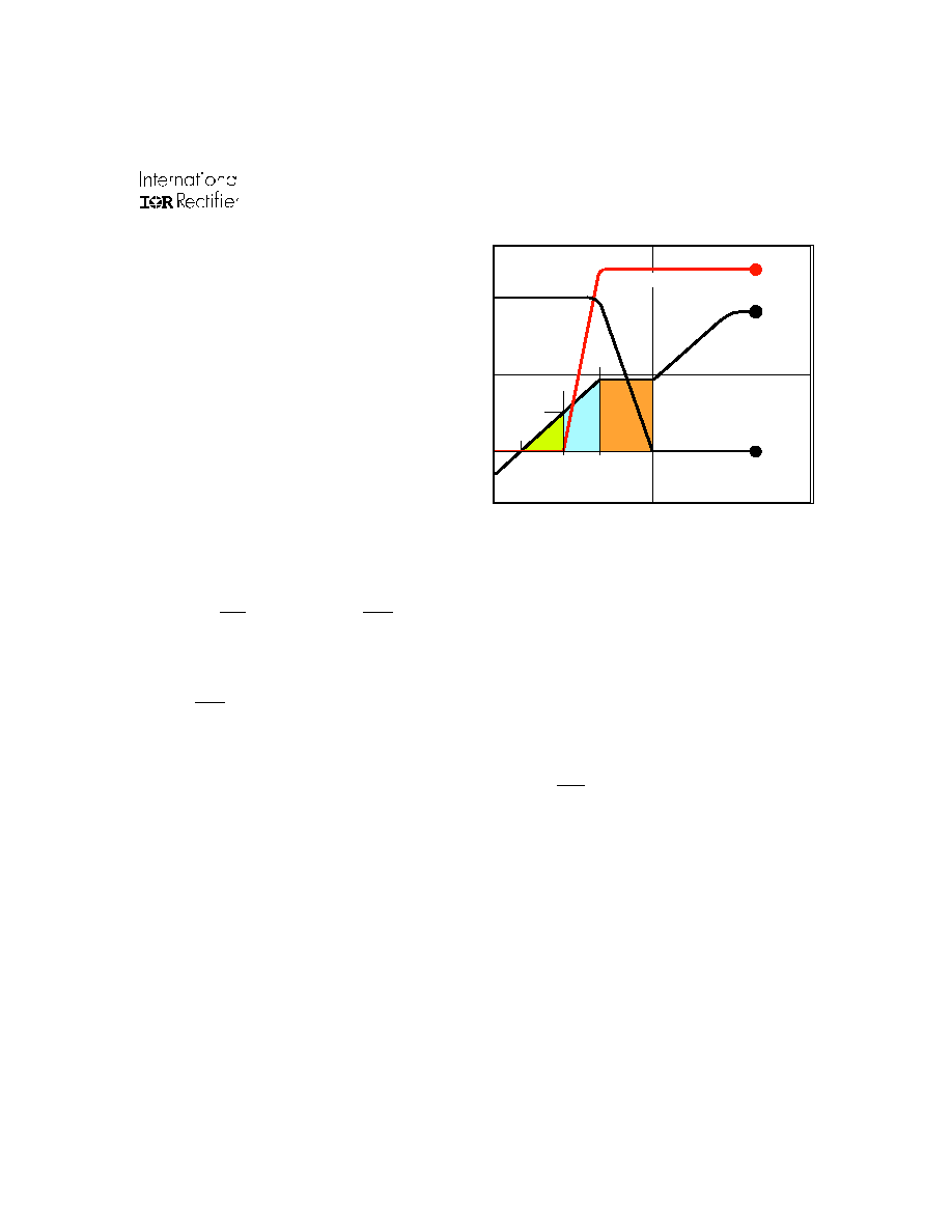
Fig 1.
Q
gs2
indicates the charge that must be supplied by
the gate driver between the time that the threshold
voltage has been reached (t1) and the time the drain
current rises to I
dmax
(t2) at which time the drain volt-
age begins to change. Minimizing Q
gs2
is a critical fac-
tor in reducing switching losses in Q1.
Q
oss
is the charge that must be supplied to the out-
put capacitance of the MOSFET during every switch-
ing cycle. Figure 2 shows how Q
oss
is formed by the
parallel combination of the voltage dependant (non-
linear) capacitance's C
ds
and C
dg
when multiplied by
the power supply input buss voltage.
Figure 1: Typical MOSFET switching waveform
Synchronous FET
The power loss equation for Q2 is approximated
by;
P
loss
=
P
conduction
+
P
drive
+
P
output
*
P
loss
=
I
rms
2
×
R
ds(on)
(
)
+
Q
g
×
V
g
×
f
(
)
+
Q
oss
2
×
V
in
×
f
+
Q
rr
×
V
in
×
f
(
)
*dissipated primarily in Q1.
Power MOSFET Selection for DC/DC
Converters
4
1
2
Drain Current
Gate Voltage
Drain Voltage
t3
t2
t1
V
GTH
Q
GS1
Q
GS2
Q
GD
t0
IRF7807V
4
www.irf.com
Typical Mobile PC Application
The performance of these new devices has been tested
in circuit and correlates well with performance predic-
tions generated by the system models. An advantage of
this new technology platform is that the MOSFETs it
produces are suitable for both control FET and synchro-
nous FET applications. This has been demonstrated with
the 3.3V and 5V converters. (Fig 3 and Fig 4). In these
applications the same MOSFET IRF7807V was used for
both the control FET (Q1) and the synchronous FET
(Q2). This provides a highly effective cost/performance
solution.
Figure 3
Figure 4
Figure 2: Q
oss
Characteristic
For the synchronous MOSFET Q2, R
ds(on)
is an im-
portant characteristic; however, once again the im-
portance of gate charge must not be overlooked since
it impacts three critical areas. Under light load the
MOSFET must still be turned on and off by the con-
trol IC so the gate drive losses become much more
significant. Secondly, the output charge Q
oss
and re-
verse recovery charge Q
rr
both generate losses that
are transfered to Q1 and increase the dissipation in
that device. Thirdly, gate charge will impact the
MOSFETs' susceptibility to Cdv/dt turn on.
The drain of Q2 is connected to the switching node
of the converter and therefore sees transitions be-
tween ground and V
in
. As Q1 turns on and off there is
a rate of change of drain voltage dV/dt which is ca-
pacitively coupled to the gate of Q2 and can induce
a voltage spike on the gate that is sufficient to turn
the MOSFET on, resulting in shoot-through current .
The ratio of Q
gd
/Q
gs1
must be minimized to reduce the
potential for Cdv/dt turn on.
Spice model for IRF7807V can be downloaded in
machine readable format at www.irf.com.
3.3V Supply : Q1=Q2= IRF7807V
5.0V Supply : Q1=Q2= IRF7807V
83
84
85
86
87
88
89
90
91
92
93
1
2
3
4
5
Load current (A)
Efficiency (%)
Vin=24V
Vin=14V
Vin=10V
86
87
88
89
90
91
92
93
94
95
1
2
3
4
5
Load cu rren t (A)
Efficiency (%)
Vin =24V
Vin =14V
Vin =10V
IRF7807V
www.irf.com
5
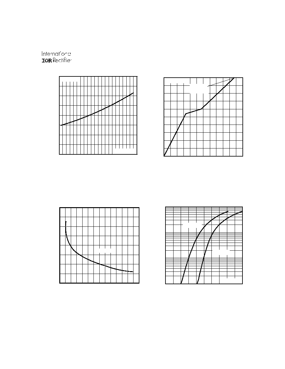
Fig 5. Normalized On-Resistance
Vs. Temperature
Fig 6. Typical Gate Charge Vs.
Gate-to-Source Voltage
Fig 7. On-Resistance Vs. Gate Voltage
Fig 8. Typical Source-Drain Diode
Forward Voltage
-60 -40 -20
0
20
40
60
80 100 120 140 160
0.0
0.5
1.0
1.5
2.0
T , Junction Temperature ( C)
R , Drain-to-Source On Resistance
(Normalized)
J
DS(on)
°
V
=
I =
GS
D
4.5V
7.0A
0
2
4
6
8
10
12
0
1
2
3
4
5
Q , Total Gate Charge (nC)
V , Gate-to-Source Voltage (V)
G
GS
I =
D
7.0A
V
= 16V
DS
0.1
1
10
100
0.2
0.4
0.6
0.8
1.0
1.2
V ,Source-to-Drain Voltage (V)
I , Reverse Drain Current (A)
SD
SD
V = 0 V
GS
T = 25 C
J
°
T = 150 C
J
°
2.0
4.0
6.0
8.0
10.0
12.0
14.0
16.0
VGS, Gate -to -Source Voltage (V)
0.010
0.015
0.020
0.025
0.030
R
DS(on)
, Drain-to -Source On Resistance (
)
ID = 7.0A