Parameter
Max.
Units
V
CES
Collector-to-Emitter Voltage
600
V
I
C
@ T
C
= 25∞C
Continuous Collector Current
8.5
I
C
@ T
C
= 100∞C
Continuous Collector Current
5.0
A
I
CM
Pulsed Collector Current
34
I
LM
Clamped Inductive Load Current
34
V
GE
Gate-to-Emitter Voltage
±20
V
E
ARV
Reverse Voltage Avalanche Energy
110
mJ
P
D
@ T
C
= 25∞C
Maximum Power Dissipation
38
P
D
@ T
C
= 100∞C
Maximum Power Dissipation
15
T
J
Operating Junction and
-55 to +150
T
STG
Storage Temperature Range
∞C
Soldering Temperature, for 10 sec.
300 (0.063 in. (1.6mm) from case )
IRG4RC10U
UltraFast Speed IGBT
INSULATED GATE BIPOLAR TRANSISTOR
PD - 91572A
E
C
G
n-channel
Features
Features
Features
Features
Features
∑ UltraFast: Optimized for high operating
frequencies ( 8-40 kHz in hard switching, >200
kHz in resonant mode)
∑ Generation 4 IGBT design provides tighter
parameter distribution and higher efficiency than
previous generation
∑ Industry standard TO-252AA package
∑ Generation 4 IGBT's offer highest efficiency available
∑ IGBT's optimized for specified application conditions
Benefits
V
CES
= 600V
V
CE(on) typ.
=
2.15V
@V
GE
= 15V, I
C
= 5.0A
8/30/99
Absolute Maximum Ratings
W
∞C/W
Parameter
Typ.
Max.
Units
R
JC
Junction-to-Case
≠≠≠
3.3
R
JA
Junction-to-Ambient (PCB mount)*
≠≠≠
50
Wt
Weight
0.3 (0.01)
≠≠≠
g (oz)
Thermal Resistance
* When mounted on 1" square PCB (FR-4 or G-10 Material).
For recommended footprint and soldering techniques refer to application note #AN-9
94
D-PAK
TO-252AA
www.irf.com
1

IRG4RC10U
2
www.irf.com
Pulse width
80µs; duty factor
0.1%.
Pulse width 5.0µs, single shot.
Notes:
Repetitive rating; V
GE
= 20V, pulse width limited by
max. junction temperature. ( See fig. 13b )
V
CC
= 80%(V
CES
), V
GE
= 20V, L = 10µH, R
G
= 100
,
(See fig. 13a)
Repetitive rating; pulse width limited by maximum
junction temperature.
Parameter
Min. Typ. Max. Units
Conditions
V
(BR)CES
Collector-to-Emitter Breakdown Voltage
600
--
--
V
V
GE
= 0V, I
C
= 250µA
V
(BR)ECS
Emitter-to-Collector Breakdown Voltage
14
--
--
V
V
GE
= 0V, I
C
= 1.0A
V
(BR)CES
/
T
J
Temperature Coeff. of Breakdown Voltage
--
0.54
--
V/∞C
V
GE
= 0V, I
C
= 1.0mA
--
2.15
2.6
I
C
= 5.0A V
GE
= 15V
V
CE(ON)
Collector-to-Emitter Saturation Voltage
--
2.61
--
I
C
= 8.5A
See Fig.2, 5
--
2.30
--
I
C
= 5.0A , T
J
= 150∞C
V
GE(th)
Gate Threshold Voltage
3.0
--
6.0
V
CE
= V
GE
, I
C
= 250µA
V
GE(th)
/
T
J
Temperature Coeff. of Threshold Voltage
--
-8.7
--
mV/∞C V
CE
= V
GE
, I
C
= 250µA
g
fe
Forward Transconductance
2.8
4.2
--
S
V
CE
=
100V, I
C
= 5.0A
--
--
250
V
GE
= 0V, V
CE
= 600V
--
--
2.0
µA
V
GE
= 0V, V
CE
= 10V, T
J
= 25∞C
--
--
1000
V
GE
= 0V, V
CE
= 600V, T
J
= 150∞C
I
GES
Gate-to-Emitter Leakage Current
--
--
±100
nA
V
GE
= ±20V
Electrical Characteristics @ T
J
= 25∞C (unless otherwise specified)
I
CES
Zero Gate Voltage Collector Current
V
Parameter
Min. Typ. Max. Units
Conditions
Q
g
Total Gate Charge (turn-on)
--
15
22
I
C
= 5.0A
Q
ge
Gate - Emitter Charge (turn-on)
--
2.6
4.0
nC
V
CC
= 400V
See Fig. 8
Q
gc
Gate - Collector Charge (turn-on)
--
5.8
8.7
V
GE
= 15V
t
d(on)
Turn-On Delay Time
--
19
--
t
r
Rise Time
--
11
--
T
J
= 25∞C
t
d(off)
Turn-Off Delay Time
--
116
240
I
C
= 5.0A, V
CC
= 480V
t
f
Fall Time
--
81
180
V
GE
= 15V, R
G
= 100
E
on
Turn-On Switching Loss
--
0.08
--
Energy losses include "tail"
E
off
Turn-Off Switching Loss
--
0.16
--
mJ
See Fig. 9, 10, 14
E
ts
Total Switching Loss
--
0.24 0.36
t
d(on)
Turn-On Delay Time
--
18
--
T
J
= 150∞C,
t
r
Rise Time
--
14
--
I
C
= 5.0A, V
CC
= 480V
t
d(off)
Turn-Off Delay Time
--
180
--
V
GE
= 15V, R
G
= 100
t
f
Fall Time
--
150
--
Energy losses include "tail"
E
ts
Total Switching Loss
--
0.36
--
mJ
See Fig. 11, 14
L
E
Internal Emitter Inductance
--
7.5
--
nH
Measured 5mm from package
C
ies
Input Capacitance
--
270
--
V
GE
= 0V
C
oes
Output Capacitance
--
21
--
pF
V
CC
= 30V
See Fig. 7
C
res
Reverse Transfer Capacitance
--
3.5
--
= 1.0MHz
Switching Characteristics @ T
J
= 25∞C (unless otherwise specified)
ns
ns
IRG4RC10U
www.irf.com
3
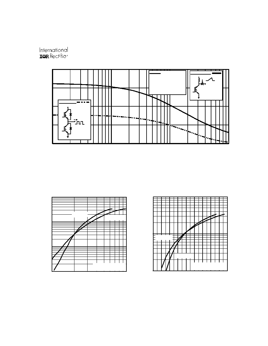
Fig. 1 - Typical Load Current vs. Frequency
(Load Current = I
RMS
of fundamental)
Fig. 2 - Typical Output Characteristics
Fig. 3 - Typical Transfer Characteristics
1
10
100
5
6
7
8
9
10
11
12
13
14
V , Gate-to-Emitter Voltage (V)
I , Collector-to-Emitter Current (A)
GE
C
V = 50V
5µs PULSE WIDTH
CC
T = 25 C
J
o
T = 150 C
J
o
Load Current ( A )
0 . 0
1 . 0
2 . 0
3 . 0
4 . 0
0 . 1
1
1 0
1 0 0
f, Frequency (kHz)
A
6 0% o f r ate d
v o lta g e
I
Ide al d io des
S q u are w ave:
F or b ot h:
T ria ng u la r w av e:
I
C lam p vo lta g e:
80% o f r ate d
P ow e r D is s ip at i on = 1 .4 W
Typ ic al F R -4 b oa rd m o u n t
D uty c ycle : 5 0%
T = 1 25 ∞C
T = 5 5∞C
G a te dri ve as s p e cified
A
J
0.1
1
10
100
1
10
V , Collector-to-Emitter Voltage (V)
I , Collector-to-Emitter Current (A)
CE
C
V = 15V
20µs PULSE WIDTH
GE
T = 25 C
J
o
T = 150 C
J
o

IRG4RC10U
4
www.irf.com
Fig. 6 - Maximum Effective Transient Thermal Impedance, Junction-to-Case
Fig. 5 - Typical Collector-to-Emitter Voltage
vs. Junction Temperature
Fig. 4 - Maximum Collector Current vs. Case
Temperature
-60 -40 -20
0
20
40
60
80 100 120 140 160
1.0
2.0
3.0
4.0
5.0
T , Junction Temperature ( C)
V , Collector-to-Emitter Voltage(V)
J
∞
CE
V = 15V
80 us PULSE WIDTH
GE
I = A
2.5
C
I = A
5
C
I = A
10
C
25
50
75
100
125
150
0
2
4
6
8
10
T , Case Temperature ( C)
Maximum DC Collector Current(A)
C
∞
5.0 A
0.01
0.1
1
10
0.00001
0.0001
0.001
0.01
0.1
1
Notes:
1. Duty factor D = t / t
2. Peak T = P
x Z
+ T
1
2
J
DM
thJC
C
P
t
t
DM
1
2
t , Rectangular Pulse Duration (sec)
Thermal Response (Z )
1
thJC
0.01
0.02
0.05
0.10
0.20
D = 0.50
SINGLE PULSE
(THERMAL RESPONSE)

IRG4RC10U
www.irf.com
5
Fig. 7 - Typical Capacitance vs.
Collector-to-Emitter Voltage
Fig. 8 - Typical Gate Charge vs.
Gate-to-Emitter Voltage
Fig. 9 - Typical Switching Losses vs. Gate
Resistance
Fig. 10 - Typical Switching Losses vs.
Junction Temperature
0
4
8
12
16
0
4
8
12
16
20
Q , Total Gate Charge (nC)
V , Gate-to-Emitter Voltage (V)
G
GE
V
= 400V
I
= 5.0A
CC
C
-60 -40 -20
0
20
40
60
80 100 120 140 160
0.01
0.1
1
10
T , Junction Temperature ( C )
Total Switching Losses (mJ)
J
∞
R = 100Ohm
V = 15V
V = 480V
G
GE
CC
I = A
10
C
I = A
5
C
I = A
2.5
C
100
5.0 A
1
10
100
0
100
200
300
400
500
V , Collector-to-Emitter Voltage (V)
C, Capacitance (pF)
CE
V
C
C
C
=
=
=
=
0V,
C
C
C
f = 1MHz
+ C
+ C
C SHORTED
GE
ies
ge
gc ,
ce
res
gc
oes
ce
gc
Cies
Coes
Cres
50
60
70
80
90
100
0.10
0.14
0.18
0.22
0.26
0.30
R , Gate Resistance (Ohm)
Total Switching Losses (mJ)
G
V = 480V
V = 15V
T = 25 C
I = 5.0A
CC
GE
J
C
∞
R
G
, Gate Resistance
(
)