Äîêóìåíòàöèÿ è îïèñàíèÿ www.docs.chipfind.ru
Absolute Maximum Ratings
Parameter
Units
ID @ VGS = -4.5V, TC = 25°C Continuous Drain Current
-1.6
ID @ VGS = -4.5V, TC = 100°C Continuous Drain Current
-1.0
IDM
Pulsed Drain Current
-6.4
PD @ TC = 25°C
Max. Power Dissipation
5.0
W
Linear Derating Factor
0.04
W/°C
VGS
Gate-to-Source Voltage
±10
V
EAS
Single Pulse Avalanche Energy
10
mJ
IAR
Avalanche Current
-1.6
A
EAR
Repetitive Avalanche Energy
0.5
mJ
dv/dt
Peak Diode Recovery dv/dt
-4.0
V/ns
T J
Operating Junction
-55 to 150
TSTG
Storage Temperature Range
Lead Temperature
300 (0.063in/1.6mm from case for 10s)
Weight
0.98 ( Typical )
g
Pre-Irradiation
o
C
A
RADIATION HARDENED
IRHLF6970Z4
LOGIC LEVEL POWER MOSFET
THRU-HOLE (TO-39)
07/07/03
www.irf.com
1
60V, P-CHANNEL
TECHNOLOGY
Product Summary
Part Number Radiation Level R
DS(on)
I
D
IRHLF6970Z4 100K Rads (Si) 1.2
-1.6A
IRHLF6930Z4 300K Rads (Si) 1.2
-1.6A
For footnotes refer to the last page
T0-39
Features:
n
5V CMOS and TTL Compatible
n
Fast Switching
n
Single Event Effect (SEE) Hardened
n
Low Total Gate Charge
n
Simple Drive Requirements
n
Ease of Paralleling
n
Hermetically Sealed
n
Light Weight
n
Complimentary N-Channel Available -
IRHLF670Z4
International Rectifier's R6
TM
Logic Level Power
Mosfets provide simple solution to interfacing CMOS
and TTL control circuits to power devices in space
and other radiation environments. The threshold
voltage remains within accptable operating limits
over the full operating temperature and post radia-
tion. This is achieved while maintaining single event
gate rupture and single event burnout immunity.
These devices are used in applications such as cur-
rent boost low signal source in PWM, voltage com-
parator and operational amplifiers.
PD - 94685

IRHLF6970Z4
Pre-Irradiation
2
www.irf.com
For footnotes refer to the last page
Source-Drain Diode Ratings and Characteristics
Parameter
Min Typ Max Units
Test Conditions
IS
Continuous Source Current (Body Diode)
--
--
-1.6
ISM
Pulse Source Current (Body Diode)
--
--
-6.4
VSD
Diode Forward Voltage
--
--
-5.0
V
T
j
= 25°C, IS = -1.6A, VGS = 0V
trr
Reverse Recovery Time
--
--
50
ns
Tj = 25°C, IF =-1.6A, di/dt
-100A/
µ
s
QRR Reverse Recovery Charge
--
--
50
nC
VDD
-25V
ton
Forward Turn-On Time
Intrinsic turn-on time is negligible. Turn-on speed is substantially controlled by LS + LD.
A
Electrical Characteristics
@ Tj = 25°C (Unless Otherwise Specified)
Parameter
Min
Typ
Max Units
Test Conditions
BVDSS
Drain-to-Source Breakdown Voltage
-60
--
--
V
VGS = 0V, ID = -250
µ
A
BVDSS/
TJ Temperature Coefficient of Breakdown
--
-0.06
--
V/°C
Reference to 25°C, ID = -1.0mA
Voltage
RDS(on)
Static Drain-to-Source On-State
--
--
1.2
VGS = -4.5V, ID = -1.0A
Resistance
VGS(th)
Gate Threshold Voltage
-1.0
--
-2.0
V
VDS = VGS, ID = -250
µ
A
gfs
Forward Transconductance
1.0
--
--
S (
)
VDS = -10V, IDS = -1.0A
IDSS
Zero Gate Voltage Drain Current
--
--
-1.0 VDS= -48V ,VGS=0V
--
--
-10
VDS = -48V,
VGS = 0V, TJ =125°C
IGSS
Gate-to-Source Leakage Forward
--
--
-100
VGS = -10V
IGSS
Gate-to-Source Leakage Reverse
--
--
100
VGS =10V
Qg
Total Gate Charge
--
--
4.0
VGS = -5.0V, ID = -1.6A
Qgs
Gate-to-Source Charge
--
--
1.5
nC
VDS = -30V
Qgd
Gate-to-Drain (`Miller') Charge
--
--
1.8
td
(on)
Turn-On Delay Time
--
--
18
VDD = -30V, ID = -1.6A,
tr
Rise Time
--
-- 20 VGS =-5.0V, RG = 24
td
(off)
Turn-Off Delay Time
--
--
15
tf
Fall Time
--
--
25
LS + LD
Total Inductance
--
7.0 --
Measured from Drain lead (6mm /0.25in
from package) to Source lead(6mm/0.25in
from packge)with Source wire internally
bonded from Source pin to Drain pad
Ciss
Input Capacitance
--
177
--
VGS = 0V, VDS = -25V
Coss
Output Capacitance
--
40
--
pF
f = 1.0MHz
Crss
Reverse Transfer Capacitance
--
8.0
--
nA
nH
ns
µ
A
Rg Gate Resistance
-- 28 --
f = 5.0MHz, open drain
Thermal Resistance
Parameter
Min Typ Max
Units
Test Conditions
RthJC
Junction-to-Case
--
--
25
°C/W
Note: Corresponding Spice and Saber models are available on International Rectifier Web site.
www.irf.com
3
Pre-Irradiation
IRHLF6970Z4
Table 1. Electrical Characteristics @ Tj = 25°C, Post Total Dose Irradiation
Parameter
100K Rads(Si)
1
300KRads(Si)
2
Units
Test Conditions
Min Max Min Max
BV
DSS
Drain-to-Source Breakdown Voltage -60 -- -60 -- V V
GS
= 0V, I
D
= -250µA
V
GS(th)
Gate Threshold Voltage
-1.0 -2.0 -1.0 -2.0
V
GS
= V
DS
, I
D
= -250µA
I
GSS
Gate-to-Source Leakage Forward
-- -100 -- -100 nA
V
GS
=-10V
I
GSS
Gate-to-Source Leakage Reverse
-- 100 -- 100
V
GS
= 10 V
I
DSS
Zero Gate Voltage Drain Current
-- -1.0 -- -10 µA V
DS
=-48V, V
GS
=0V
R
DS(on)
Static Drain-to-Source
-- 1.2 -- 1.2
V
GS
= -4.5V, I
D
=-1.0A
On-State Resistance (TO-39)
International Rectifier Radiation Hardened MOSFETs are tested to verify their radiation hardness capability.
The hardness assurance program at International Rectifier is comprised of two radiation environments.
Every manufacturing lot is tested for total ionizing dose (per notes 5 and 6) using the TO-3 package. Both
pre- and post-irradiation performance are tested and specified using the same drive circuitry and test
conditions in order to provide a direct comparison.
Radiation Characteristics
1. Part number IRHLF6970Z4
2. Part number IRHLF6930Z4
International Rectifier radiation hardened MOSFETs have been characterized in heavy ion environment for
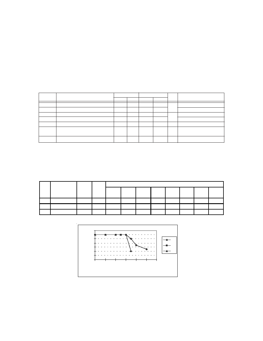
Single Event Effects (SEE). Single Event Effects characterization is illustrated in Fig. a and Table 2.
Fig a. Single Event Effect, Safe Operating Area
For footnotes refer to the last page
Table 2. Single Event Effect Safe Operating Area
Ion
LET
Energy Range
VDS (V)
(MeV/(mg/cm2))
(MeV)
(µm)
@VGS=
@VGS= @VGS= @VGS= @VGS= @VGS= @VGS= @VGS=
0V
2V
4V
5V
6V
7V
8V
10V
Br
37.9
285
36.8
-60
-60
-60
-60
-60
-50
-35
-25
I
59.9
345
32.7
-60
-60
-60
-60
-60
-20
-
-
Au
82.3
357
28.5
-60
-60
-60
-60
-
-
-
-
-70
-60
-50
-40
-30
-20
-10
0
0
2
4
6
8
10
12
VGS
VD
S
Br
I
Au
V
SD
Diode Forward Voltage
-- -5.0
-- -5.0 V
V
GS
= 0V, IS = -1.6A

IRHLF6970Z4
Pre-Irradiation
4
www.irf.com
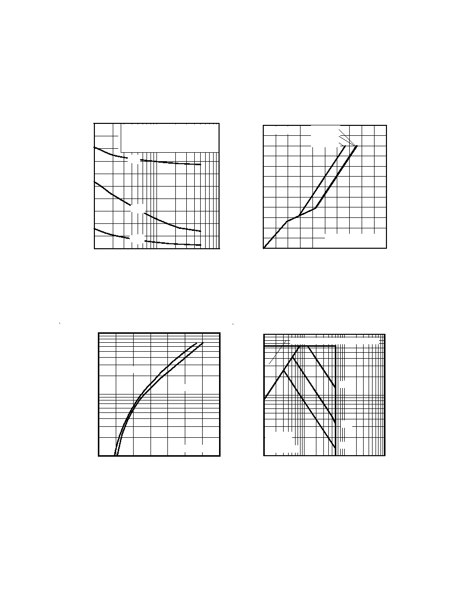
Fig 4. Normalized On-Resistance
Vs. Temperature
Fig 2. Typical Output Characteristics
Fig 1. Typical Output Characteristics
Fig 3. Typical Transfer Characteristics
15
1
2
3
4
5
6
7
8
-VGS, Gate-to-Source Voltage (V)
0.1
1
10
-I
D
, Drain-to-Source Current (
)
VDS = -25V
60µs PULSE WIDTH
TJ = 150°C
TJ = 25°C
0.1
1
10
100
-VDS , Drain-to-Source Voltage (V)
0.1
1
10
-I
D
, Drain-to-Source Current (A)
60µs PULSE WIDTH
Tj = 150°C
-
2.25V
VGS
TOP -10V
-7.5V
-5.0V
-4.0V
-3.5V
-3.0V
-2.5V
BOTTOM -2.25V
0.1
1
10
100
-VDS , Drain-to-Source Voltage (V)
0.1
1
10
-I
D
, Drain-to-Source Current (A)
60µs PULSE WIDTH
Tj = 25°C
VGS
TOP -10V
-7.5V
-5.0V
-4.0V
-3.5V
-3.0V
-2.5V
BOTTOM -2.25V
-
2.25V
-60 -40 -20
0
20
40
60
80 100 120 140 160
0.0
0.5
1.0
1.5
2.0
T , Junction Temperature ( C)
R , Drain-to-Source On Resistance
(Normalized)
J
DS(on)
°
V
=
I =
GS
D
-4.5V
-1.6A
www.irf.com
5
Pre-Irradiation
IRHLF6970Z4
Fig 8. Maximum Safe Operating Area
Fig 6. Typical Gate Charge Vs.
Gate-to-Source Voltage
Fig 5. Typical Capacitance Vs.
Drain-to-Source Voltage
Fig 7. Typical Source-Drain Diode
Forward Voltage
1
10
100
0
50
100
150
200
250
-V , Drain-to-Source Voltage (V)
C, Capacitance (pF)
DS
V
C
C
C
=
=
=
=
0V,
C
C
C
f = 1MHz
+ C
+ C
C SHORTED
GS
iss
gs
gd ,
ds
rss
gd
oss
ds
gd
Ciss
Coss
Crss
0
1
2
3
4
5
0
2
4
6
8
10
12
Q , Total Gate Charge (nC)
-V , Gate-to-Source Voltage (V)
G
GS
FOR TEST CIRCUIT
SEE FIGURE
I =
D
13
-1.6A
V
= -12V
DS
V
= -30V
DS
V
= -48V
DS
1
10
100
1000
-VDS , Drain-to-Source Voltage (V)
0.1
1
10
-I
D
, Drain-to-Source Current (A)
Tc = 25°C
Tj = 150°C
Single Pulse
1ms
10ms
OPERATION IN THIS AREA LIMITED
100µs
BY RDS(on)
0
1
2
3
4
5
6
7
-VSD , Source-to-Drain Voltage (V)
0.1
1
10
-I
SD
, Reverse Drain Current (
)
VGS = 0V
TJ = 150°C
TJ = 25°C