Äîêóìåíòàöèÿ è îïèñàíèÿ www.docs.chipfind.ru

08/07/02
RAD-HARD
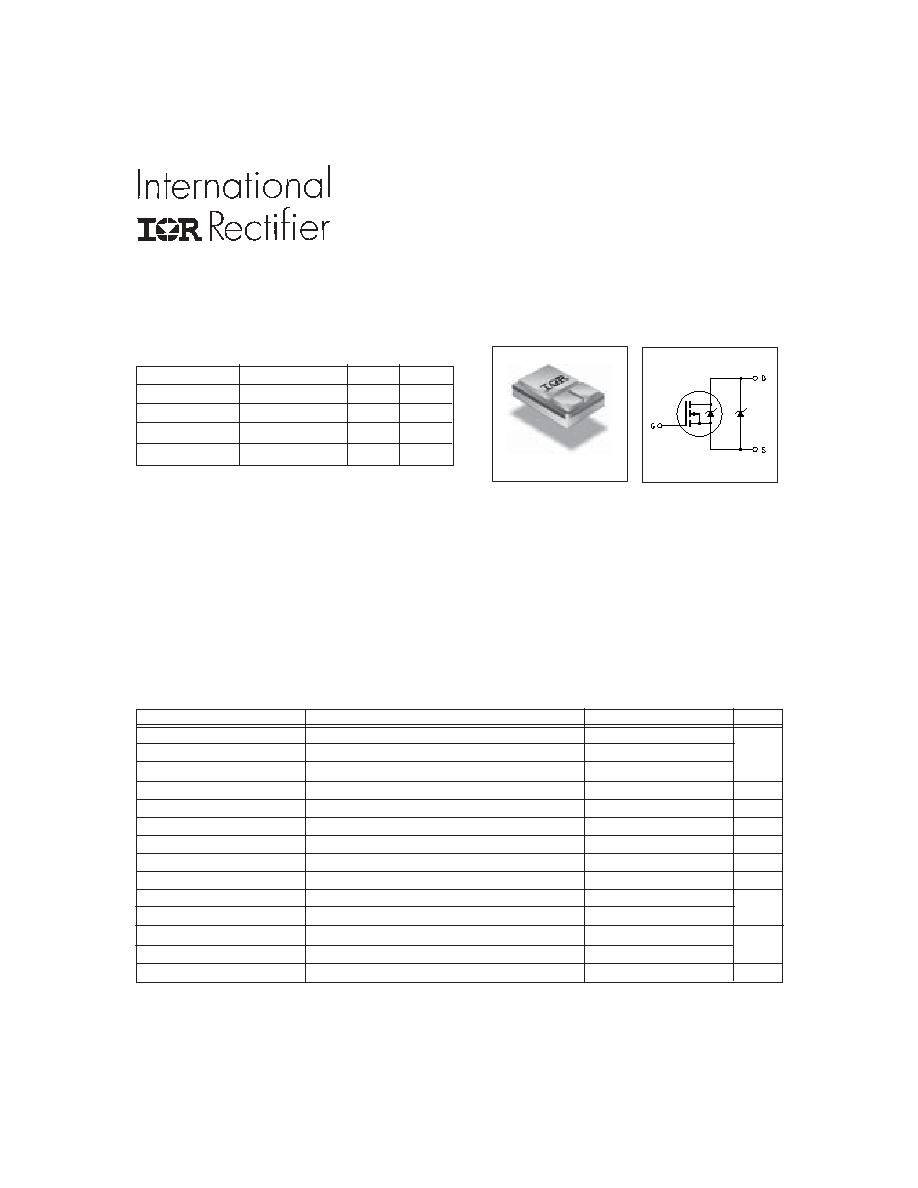
IRHSLNA57064
SYNCHRONOUS RECTIFIER
SURFACE MOUNT (SMD-2)
www.irf.com
1
60V, N-CHANNEL
Features:
n
Co-Pack N-channel RAD-Hard MOSFET
and Schottky Diode
n
Ideal for Synchronous Rectifiers in DC-DC
Converters up to 75A Output
n
Low Conduction Losses
n
Low Switching Losses
n
Low Vf Schottky Rectifier
n
Refer to IRHSNA57064 for Lower
R
DS(on)
For footnotes refer to the last page
* Current is limited by package
SMD-2
Description:
The SynchFet family of Co-Pack RAD-Hard MOSFETs
and Schottky diodes offers the designer an innovative,
board space saving solution for switching regulator and
power management applications. RAD-Hard MOSFETs
utilize advanced processing techniques to achieve
extremely low on-resistance per silicon area. Combining
this technology with International Rectifier's low forward
drop Schottky rectifiers results in an extremely efficient
device suitable for use in a wide variety of Military and
Space applications.
Product Summary
Part Number Radiation Level R
DS(on)
Q
G
IRHSLNA57064 100K Rads (Si) 6.1m
160nC
IRHSLNA53064 300K Rads (Si) 6.1m
160nC
IRHSLNA54064 600K Rads (Si) 6.1m
160nC
IRHSLNA58064 1000K Rads (Si) 7.1m
160nC
Absolute Maximum Ratings
Parameter
Units
ID @ VGS = 12V, TC = 25°C
Continuous Drain or Source Current
75*
ID @ VGS = 12V, TC = 100°C Continuous Drain or Source Current
75*
IDM
Pulsed Drain Current
300
PD @ TC = 25°C
Max. Power Dissipation
250
W
Linear Derating Factor
2.0
W/°C
VGS
Gate-to-Source Voltage
±20
V
EAS
Single Pulse Avalanche Energy
370
mJ
IAR
Avalanche Current
75
A
EAR
Repetitive Avalanche Energy
25
mJ
IF (AV)@ TC = 25°C
Schottky and Body Diode Avg. Forward Current
75*
IF (AV)@ TC =100°C
Schottky and Body Diode Avg. Forward Current
75*
TJ, TSTG
Opeating and Storage Temperature Range -55 to 150
Pckg. Mounting Surface Temp.
300 (for 5s)
Weight
3.3 (Typical)
g
Pre-Irradiation
A
A
°C
PD-94401A

IRHSLNA57064
2
www.irf.com
Pre-Irradiation
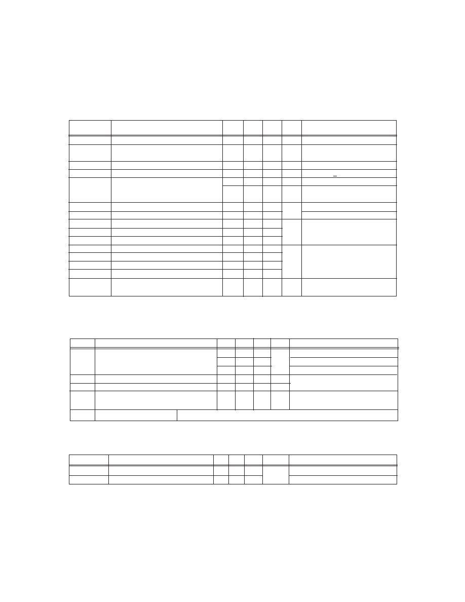
Electrical Characteristics
@ Tj = 25°C (Unless Otherwise Specified)
Parameter
Min
Typ Max Units
Test Conditions
BVDSS
Drain-to-Source Breakdown Voltage
60
--
-- V VGS = 0V, ID = 1.0mA
RDS(on)
Static Drain-to-Source On-State
--
--
6.1 m
VGS = 12V, ID = 45A
Resistance
VGS(th)
Gate Threshold Voltage
2.0
--
4.0
V VDS = VGS, ID = 1.0mA
gfs
Forward Transconductance
45
--
--
S (
)
VDS > 15V, IDS = 45A
IDSS
Zero Gate Voltage Drain Current
-- -- 50
VDS = 48V, VGS=0V
--
--
50
mA
VDS = 48V,
VGS = 0V, TJ = 125°C
IGSS
Gate-to-Source Leakage Forward
--
--
100
VGS = 20V
IGSS
Gate-to-Source Leakage Reverse
--
-- -100 VGS = -20V
Qg
Total Gate Charge
--
--
160 VGS =12V, ID =45A,
Qgs
Gate-to-Source Charge
--
--
55 nC VDS = 30V
Qgd
Gate-to-Drain (`Miller') Charge
--
--
65
td
(on)
Turn-On Delay Time
--
--
35 VDD = 30V, ID = 45A,
tr
Rise Time
--
--
125 VGS =12V, RG = 2.35
td
(off)
Turn-Off Delay Time
--
--
75
tf
Fall Time
--
--
50
LS + LD
Total Inductance
--
6.6
--
Measured from center of drain
pad to center of source pad
nA
nH
ns
µ
A
Schottky Diode & Body Diode Ratings and Characteristics
Parameter
Min Typ Max Units
Test Conditions
VSD
Diode Forward Voltage
--
--
0.93
TJ = -55°C, ID=45A, VGS = 0V
--
--
0.9
TJ = 25°C, ID= 45A, VGS = 0V
--
--
0.82
TJ = 125°C, ID=45A, VGS = 0V
trr
Reverse Recovery Time
--
--
100
nS
Tj = 25°C, IF =45A, di/dt
100A/
µ
s
QRR
Reverse Recovery Charge
--
--
210
nC
VDS
30V
LS + LD Total Inductance
--
7.95
--
nH
Measured from center of drain pad to
center of source pad (for Schottky only)
ton
Forward Turn-On Time
Intrinsic turn-on time is negligible. Turn-on speed is substantially controlled by LS + LD
V
Thermal Resistance
Parameter
Min Typ Max
Units
Test Conditions
RthJC
Junction-to-Case (MOSFET)
--
--
0.5
RthJC
Junction-to-Case (Schottky)
--
--
0.7
°C/W
Note: Corresponding Spice and Saber models are available on the Website.
For footnotes refer to the last page

IRHSLNA57064
www.irf.com
3
International Rectifier Radiation Hardened MOSFETs are tested to verify their radiation hardness capability.
The hardness assurance program at International Rectifier is comprised of two radiation environments.
Every manufacturing lot is tested for total ionizing dose (per notes 5 and 6) using the TO-3 package. Both
pre- and post-irradiation performance are tested and specified using the same drive circuitry and test condi-
tions in order to provide a direct comparison.
Radiation Characteristics
1. Part numbers IRHSLNA57064, IRHSLNA53064 and IRHSLNA54064
2. Part number IRHSLNA58064
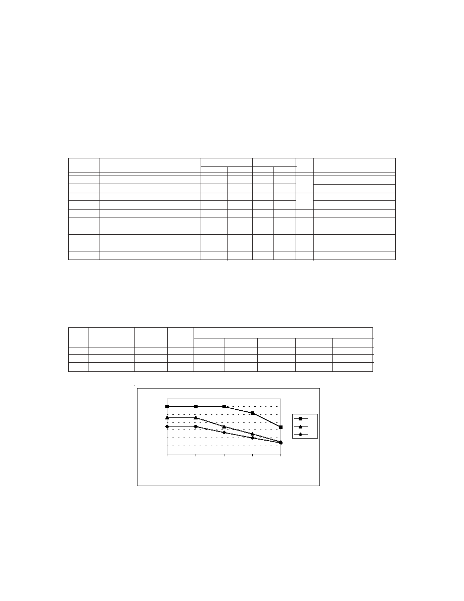
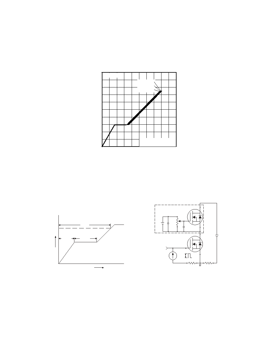
Fig a. Single Event Effect, Safe Operating Area
International Rectifier Radiation Hardened MOSFETs have been characterized in heavy ion environment for
Single Event Effects (SEE). Single Event Effects characterization is illustrated in Fig. a and Table 2.
For footnotes refer to the last page
Table 2. Single Event Effect Safe Operating Area
Ion
LET
Energy Range
V
DS
(V)
MeV/(mg/cm
2
)) (MeV) (µm) @V
GS
=0V @V
GS
=-5V @V
GS
=-10V @V
GS
=-15V @V
GS
=-20V
Kr
39.2
300 37.4 60 60 60 52 34
Xe
63.3
300 29.2 46 46 35 25 15
Au
86.6
2068 106 35 35 27
20
14
0
10
20
30
40
50
60
70
0
-5
-10
-15
-20
VGS
VDS
Kr
Xe
Au
Table 1. Electrical Characteristics @ Tj = 25°C, Post Total Dose Irradiation
Parameter
Up to 600K Rads(Si)
1
1000K Rads (Si)
2
Units
Test Conditions
Min Max Min Max
BV
DSS
Drain-to-Source Breakdown Voltage 60 -- 60 -- V V
GS
= 0V, I
D
= 1.0mA
V
GS(th)
Gate Threshold Voltage
2.0 4.0 1.5 4.0
V
GS
= V
DS
, I
D
= 1.0mA
I
GSS
Gate-to-Source Leakage Forward
-- 100 -- 100 nA
V
GS
= 20V
I
GSS
Gate-to-Source Leakage Reverse
-- -100 -- -100
V
GS
= -20 V
I
DSS
Zero Gate Voltage Drain Current
-- 10 -- 25 µA
V
DS
=48V, V
GS
=0V
R
DS(on)
Static Drain-to-Source
-- 6.1 -- 7.1
m
V
GS
= 12V, I
D
=45A
On-State Resistance (TO-3)
R
DS(on)
Static Drain-to-Source
-- 6.1 -- 7.1
m
V
GS
= 12V, I
D
=45A
On-State Resistance (SMD-2)
V
SD
Diode Forward Voltage
-- 1.3 -- 1.3 V
V
GS
= 0V, IS = 45A

IRHSLNA57064
4
www.irf.com
Pre-Irradiation
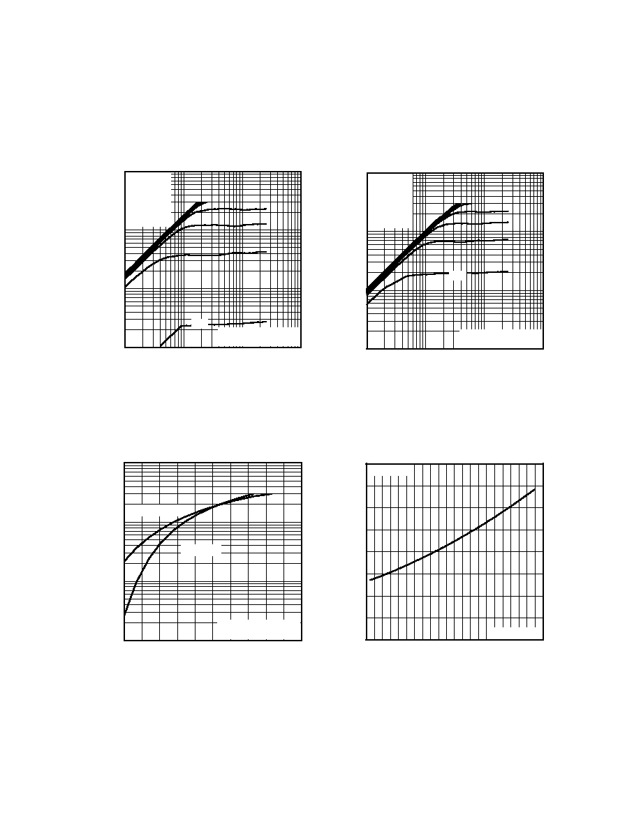
Fig 1. Typical Output Characteristics
Fig 2. Typical Output Characteristics
Fig 4. Normalized On-Resistance
Vs. Temperature
Fig 3. Typical Transfer Characteristics
1
10
100
1000
0.1
1
10
100
20µs PULSE WIDTH
T = 25 C
J
°
TOP
BOTTOM
VGS
15V
12V
10V
9.0V
8.0V
7.0V
6.0V
5.0V
V , Drain-to-Source Voltage (V)
I , Drain-to-Source Current (A)
DS
D
5.0V
1
10
100
1000
0.1
1
10
100
20µs PULSE WIDTH
T = 150 C
J
°
TOP
BOTTOM
VGS
15V
12V
10V
9.0V
8.0V
7.0V
6.0V
5.0V
V , Drain-to-Source Voltage (V)
I , Drain-to-Source Current (A)
DS
D
5.0V
1
10
100
1000
5.0
6.0
7.0
8.0
9.0
10.0
V = 25V
20µs PULSE WIDTH
DS
V , Gate-to-Source Voltage (V)
I , Drain-to-Source Current (A)
GS
D
T = 25 C
J
°
T = 150 C
J
°
-60 -40 -20
0
20
40
60
80 100 120 140 160
0.0
0.5
1.0
1.5
2.0
T , Junction Temperature ( C)
R , Drain-to-Source On Resistance
(Normalized)
J
DS(on)
°
V
=
I =
GS
D
12V
75A

IRHSLNA57064
www.irf.com
5
Fig 5. Typical Gate Charge Vs.
Gate-to-Source Voltage
D.U.T.
V
DS
I
D
I
G
3mA
V
GS
.3
µ
F
50K
.2
µ
F
12V
Current Regulator
Same Type as D.U.T.
Current Sampling Resistors
+
-
Fig 5b. Gate Charge Test Circuit
Q
G
Q
GS
Q
GD
V
G
Charge
12 V
Fig 5a. Basic Gate Charge Waveform
0
50
100
150
200
250
0
4
8
12
16
20
Q , Total Gate Charge (nC)
V , Gate-to-Source Voltage (V)
G
GS
FOR TEST CIRCUIT
SEE FIGURE
I =
D
13
45A
V
= 12V
DS
V
= 30V
DS
V
= 48V
DS
Pre-Irradiation
5b
