 | ÐлекÑÑоннÑй компоненÑ: IRISMPS3 | СкаÑаÑÑ:  PDF PDF  ZIP ZIP |
Äîêóìåíòàöèÿ è îïèñàíèÿ www.docs.chipfind.ru

www.irf.com
1
IRISMPS3
International Rectifier
·
233 Kansas Street El Segundo CA 90245 USA
Technical Specifications
1. AC Input: V=90~265V, f=57~63Hz, I= 1.3Arms max
2. Inrush Current: 13A max
3. Efficiency: 87% at full load high line (82% at low line)
4. Turn On Delay: <2secs @ 90V full load
5. Short Circuit Protection: Yes
6. Over Voltage Protection: Yes
7. Hold-Up Time: 140msec (230Vin Full load) / 27ms (90Vin Full load)
8. Output Rise Time: 7ms max (10-90%)
9. Output Characteristics
10: Switching Frequency: 20 -250kHz
Relevant Technical Documents
AN1018a - Using the IR40xx Series SMPS ICs
AN1024a - Flyback transformer design for the IR40xx series
AN1025a - Designing a Power Supply Using The IRIS40xx Series
DT01-1 - A Standby Circuit For the IRIS40xx Integrated Switchers
IRIStran.xls - IRIS Series Flyback Transformer Design Spreadsheet
IRIS4013(K) - Datasheet
R
EFERENCE
D
ESIGN
Nominal Ouput Voltage
Load Range
Regulation
(V)
Min
Max
15V
0A
4A
14.4V ~ 15.6V

2
www.irf.com
IRISMPS3
Circuit Description
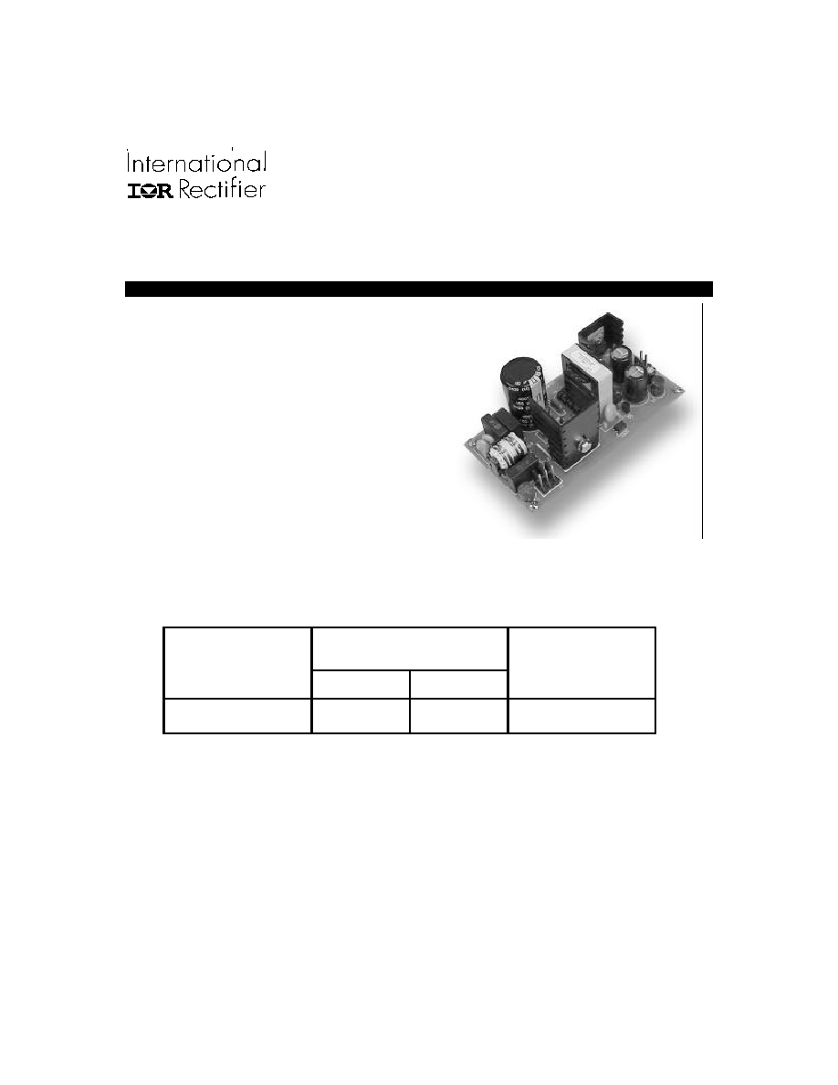
The IRISMPS3 reference design is a complete tested power supply circuit. It is designed for a universal AC
line input and will provide a 15V, 4A full load DC output.
The design uses a flyback converter topology, with an IRIS4013K as the main switch and control device. The
initial start-up current for the IRIS4013K is provided by a dropper resistor from the DC bus. Once the circuit is
started the Vcc power for the IRIS4013K comes from the bias winding of the main transformer. The primary
current control circuit consists of a current sensing resistor which feeds a voltage proportional to the transformer
primary current into the feedback (FB) pin of the IRIS4013K. The secondary voltage control loop uses an LM431
precision shunt regulator as the reference and an optocoupler to feedback the information across the transformer
galvanic isolation boundary back to the control circuit of the IRIS4013K.
Test Circuit Set-up
The circuit is designed for a universal AC line input. To safely test and evaluate this circuit it is recommended
that an isolation transformer or a synthesized and isolated AC source (such as a Pacific Power Source 115-ASX)
is used to power the board, with a voltage in the range of 90-265VAC, with a frequency of 50/60Hz. The AC input
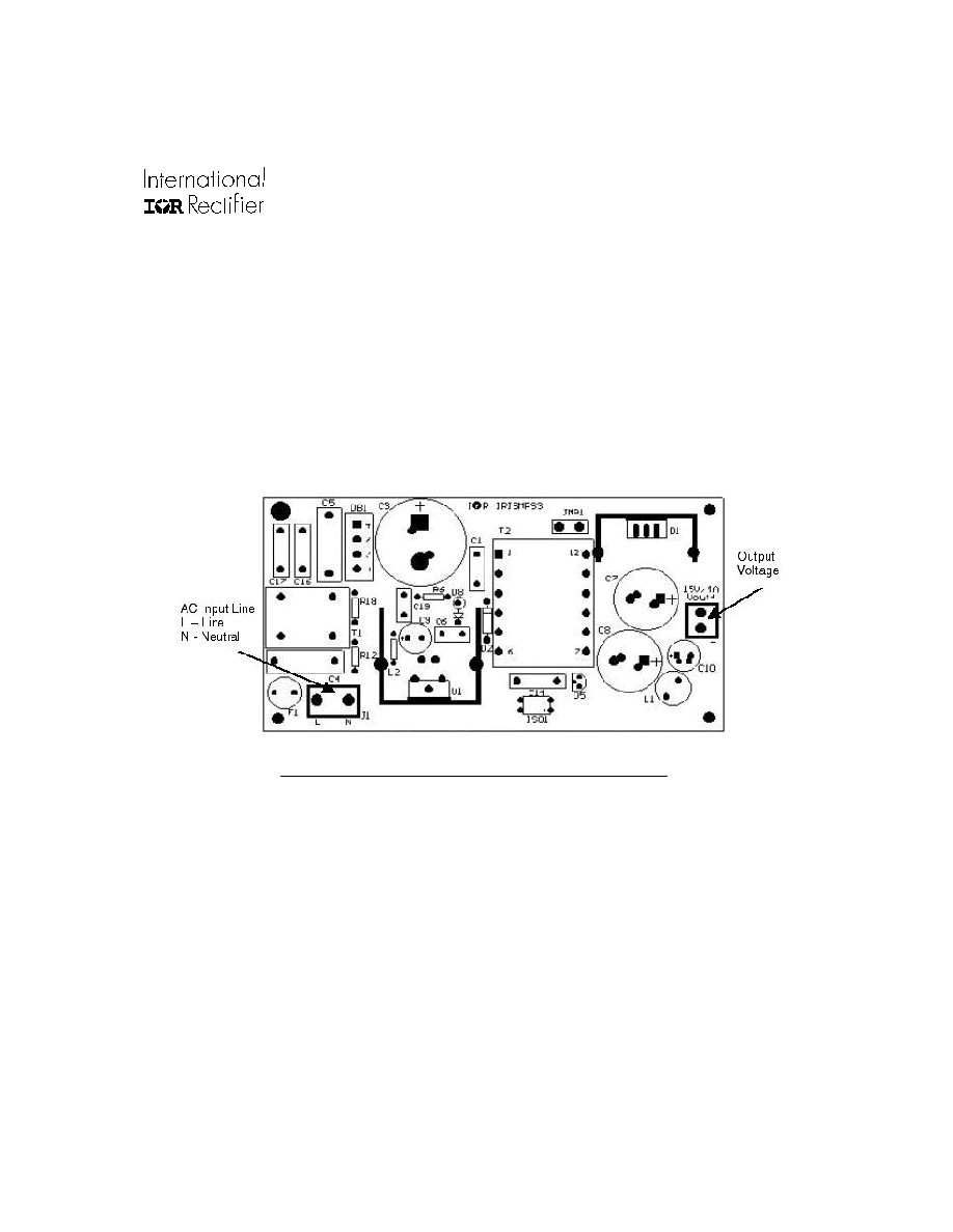
signal is applied to the pins at P1 and P3 marked on the board.
For the output the best load to use is an electronic load which will allow easy changes in the output load, e.g.
something like a Chroma 63102. Another simple alternative is to use a High power resistor for the load. The output
connection are as follows: P2 is the Positive output voltage connection, P4 is the negative(or return) output con-
nection.
Circuit Operation
The front end of the circuit consists of an EMI Filter, a diode bridge rectifier, and a DC bus filter capacitor.
These are all fairly common circuit components used to create a DC voltage at the top end of the transformer.
At power up the DC voltage is applied to the top of the transformer, and the top of resistor R2. R2 and R3 allow
Fig 1) Connections to the board viewed from the top board layout

www.irf.com
3
IRISMPS3
about 100uA of quiescent current to flow which charges the Vcc capacitor C9. When the voltage at the Vcc pin of
the IRIS4013K reaches the positive undervoltage lockout threshold (V
CCUV+
) , the IRIS4013K starts to operate and
will turn on the internal FET. Now the DC bus voltage is applied across the transformer primary winding, the FET
and the current sense resistors R15/R16. The current through the transformer primary, the FET and the current
sense resistors will start to ramp up. The rate of the ramp is dependent on the DC bus voltage and hence the input
line voltage (for example, the rate at 90VAC in is much lower than the rate at 230VAC in). The current ramps until
the voltage across R15/R16 reaches the Vth1 of the IRIS4013K (0.73V typ). During this time there is no current
flowing in either the bias winding or the output winding, because this is blocked by the diodes D3 and D1 respec-
tively.
At the point when the voltage across R15/R16 reaches Vth1 this activates a comparator in the IRIS4013K and
the internal FET is switched off. Now the energy stored in the transformer causes the voltage at the Drain con-
nected end of the transformer to rise, and as a result the voltage at the bias winding and the output winding
changes from negative to positive. The output rectifiers now conducts and the energy is transferred to the output
and the bias winding. If there is a fixed full current load on the output it will take a number of cycles for the output
voltage to rise to the required level, and also it will take a few cycles for the bias winding to begin supplying power
to the Vcc pin of the IRIS4013K. Until this happens, C9 holds the voltage above the undervoltage lockout level
(Vccuv-) to make sure the circuit does not drop out. During this time the circuit cannot create enough voltage
signal through the delay circuit to activate the quasi-resonant operation, so the circuit operates with a fixed off time
of 50us (this is the pulse ratio control mode or PRC mode).
Once the output capacitors C7 & C8 and the Vcc capacitor C9 are fully charged, the complete quasi-resonant
signal can be passed through the mode switching circuit & delay circuit D4/Q1/R11/D6 to the feedback (FB) pin
This will happen only if the Bias winding voltage is above the switching threshold of the mode switching circuit (the
operation of the mode switching circuit will be discussed in the next section). This will give a voltage above the
Vth2 threshold of the IRIS4013K, and this activates the quasi-resonant operation, holding the internal FET off until
all the energy is transferred from the primary side of the transformer to the secondary and bias outputs. When all
the energy is transferred, the quasi-resonant signal at the FB pin will start to fall until it can no longer supply the
1.35mA required by the IRIS4013K internal latch, and the FET is turned back on. This is also the lowest point of the
resonant voltage at the drain pin of the IRIS4013K (shown as point X in fig2 ), so results in reduced switching
losses.
If the AC input voltage changes but the load stays constant, the primary current ramp will now be steeper
resulting in a shorter ON time, but still the same off time as it still takes the same amount of time to transfer the
same energy to the output. The reduced ON time leads to a higher operating frequency.
If the AC input voltage remains constant, but the load is reduced, the secondary side voltage monitoring circuit
(ISO1A/R9/D5/R5/R13/C13) will see an increase in the voltage, as the circuit is still passing the same energy to
the secondary side, but less current is being drawn. This causes the LM431 Precision Shunt Regulator (D5) to
conduct, causing to a current flow in the optocoupler ISO1A, which in turn gets passed across the transformer
boundary to the phototransistor part of the optocoupler ISO1B. This creates a voltage drop across R8, generating
an offset voltage at the FB pin thereby reducing the current required through the current sense resistors R15/R16
needed to reach a voltage of 0.73typ (Vth1 threshold) at the FB pin, and hence less energy is put into the trans-
former, reducing both the ON time and the OFF time.
Mode Switching Circuit Operation
The mode switching circuit consists of Q1/R8/C12/R12/D7 and is used to switch the operating mode of the
IRIS device between quasi-resonant and PRC modes dependant on the output loading, with the aim of reducing
the power loss at light or no load.
At full load the bias winding voltage is higher than the switching threshold of the mode switching circuit which
is set at about 13V in this circuit, this results in a current through D4/R8/R12/D7 which causes enough voltage
across the base emitter junction of Q1 to forward bias it, which in turn allows the quasi-resonant signal to pass

4
www.irf.com
IRISMPS3
through R11/D6 to the FB pin of the IRIS4013K.
If the bias winding voltage is below the threshold Q1 is off and no quasi-resonant signal is passed, this causes
U1 to operate in the PRC mode with a fixed of time of 50us, this results in a further lowering of the Vcc voltage to
provide some hysteresis to prevent spurious changing between modes.
Circuit Waveforms
The following plots show waveforms taken from the circuit under various stated conditions
Fig 2) Drain (D) voltage of IRIS4013K (CH1) and FB voltage (CH3) 90VAC in Full load
Fig 2) shows the drain voltage of the IRIS4013K and the FB voltage with full load output at 90VAC input.
Note that point X marked on the drain waveform shows the detection point for the quasi-resonant signal which
is the lowest point on the drain waveform after the energy is transferred.
Fig 3) shows the drain voltage and the feedback pin (FB) voltage at 265VAC input again with a full load
output. Note that at the start of the ON time for the FET the FB pin signal has a higher dv/dt rise. This is due to
the feedback signal from the output creating the offset voltage to keep the output power constant. Also note that
the on-time is shorter and hence the operating frequency is higher.

www.irf.com
5
IRISMPS3
Fig 3)Drain (D) voltage of IRIS4013K (CH1) and the FB pin voltage (CH3) at 265VAC in/Full load output
Fig 4) Drain (D) voltage of IRIS4013K (CH1) and the Source pin voltage (CH3) at 230VAC in/Full load
output
Fig 4) shows the Drain voltage and the source pin voltage at 230VAC input an


