 | –≠–ª–µ–∫—Ç—Ä–æ–Ω–Ω—ã–π –∫–æ–º–ø–æ–Ω–µ–Ω—Ç: IRKF132 | –°–∫–∞—á–∞—Ç—å:  PDF PDF  ZIP ZIP |

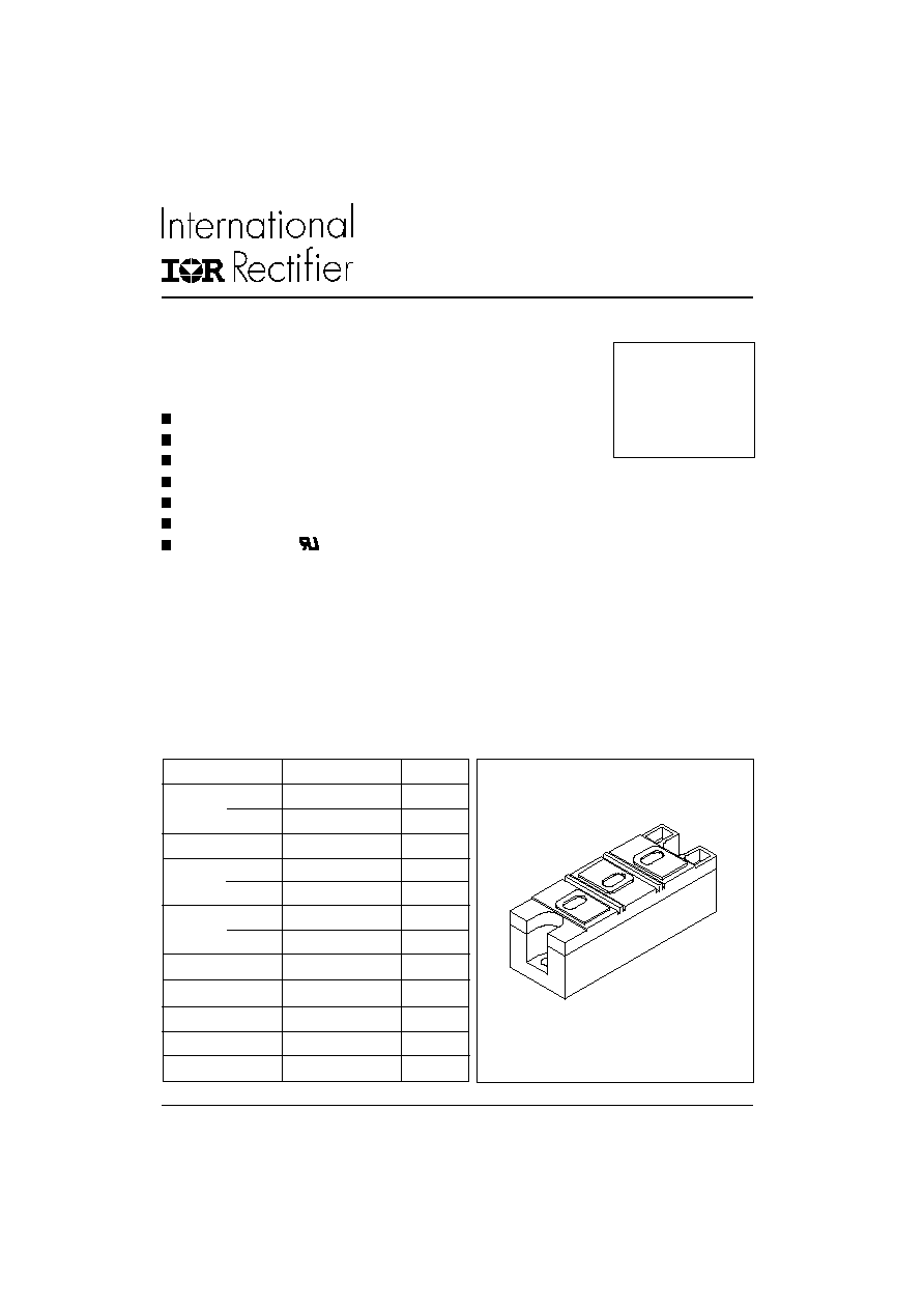
130 A
FAST THYRISTOR/ DIODE and
THYRISTOR/ THYRISTOR
Bulletin I27092 rev. A 09/97
1
IRK.F132.. SERIES
INT-A-pak
‰
Power Modules
www.irf.com
Features
Fast turn-off thyristor
Fast recovery diode
High surge capability
Electrically isolated baseplate
3000 V
RMS
isolating voltage
Industrial standard package
UL E78996 approved
Description
These series of INT-A-pak modules are intended for
applications such as self-commutated inverters, DC
choppers, electronic welders, induction heating and
others where fast switching characteristics are required.
Parameters
IRK.F132..
Units
I
T(AV)
130
A
@ T
C
90
∞C
I
T(RMS)
293
A
I
TSM
@ 50Hz
3210
A
@ 60Hz
3360
A
I
2
t
@ 50Hz
51.5
KA
2
s
@ 60Hz
47.0
KA
2
s
I
2
t
515
KA
2
s
t
q
15
µs
t
rr
2
µs
V
DRM
/ V
RRM
up to 800
V
T
J
range
- 40 to 125
o
C
Major Ratings and Characteristics

IRK.F132.. Series
2
Bulletin I27092 rev. A 09/97
www.irf.com
ELECTRICAL SPECIFICATIONS
Voltage Ratings
Voltage
V
RRM
/V
DRM
, maximum repetitive
V
RSM
, maximum non-
I
RRM
/I
DRM
max.
Type number
Code
peak reverse voltage
repetitive peak rev. voltage
@ T
J
= 125∞C
V
V
mA
04
400
400
08
800
800
I
T(AV)
Maximum average on-state current
130
A
180∞ conduction, half sine wave
@ Case temperature
90
∞C
I
T(RMS)
Maximum RMS current
293
A
T
C
= 90∞C, as AC switch
I
TSM
Maximum peak, one-cycle,
3210
A
t = 10ms
No voltage
non-repetitive surge current
3360
t = 8.3ms
reapplied
2700
t = 10ms
100% V
RRM
2825
t = 8.3ms
reapplied
Sinusoidal half wave,
I
2
t
Maximum I
2
t for fusing
51.5
KA
2
s
t = 10ms
No voltage
Initial T
J
= 125∞C
47.0
t = 8.3ms
reapplied
36.5
t = 10ms
100% V
RRM
33.3
t = 8.3ms
reapplied
I
2
t
Maximum I
2
t for fusing
515
KA
2
s t = 0 to 10ms, no voltage reapplied
V
T(TO)1
Low level value of threshold voltage
1.16
V
(16.7% x
x I
T(AV)
< I <
x I
T(AV)
), T
J
= T
J
max.
V
T(TO)2
High level value of threshold voltage
1.25
(I >
x I
T(AV)
), T
J
= T
J
max.
r
t1
Low level value of on-state slope resistance
0.92
mW
(16.7% x
x I
T(AV)
< I <
x I
T(AV)
), T
J
= T
J
max.
r
t2
High level value of on-state slope resistance
0.77
(I >
x I
T(AV)
), T
J
= T
J
max.
V
TM
Maximum on-state voltage drop
1.71
V
I
pk
= 600A, T
J
= T
J
max., t
p
= 10ms sine pulse
I
H
Maximum holding current
600
mA
T
J
= 25∞C, I
T
> 30 A
I
L
Typical latching current
1000
mA
T
J
= 25∞C, V
A
= 12V, Ra = 6
, Ig
= 1A
Parameter
IRK.F132..
Units Conditions
On-state Conduction
Frequency f
Units
50Hz
250
420
408
640
2465
3460
A
400Hz
320
530
485
800
1470
2150
A
2500Hz
240
390
400
650
540
830
A
5000Hz
210
340
340
530
340
530
A
10000Hz
160
275
300
415
-
-
A
Recovery voltage Vr
50
50
50
50
50
50
V
Voltage before turn-on Vd
80% V
DRM
80% V
DRM
80% V
DRM
V
Rise of on-state current di/dt
50
50
-
-
-
-
A/µ s
Case temperature
90
60
90
60
90
60
∞C
Equivalent values for RC circuit
47
/ 0.22 µF
47
/ 0.22 µF
47
/ 0.22 µF
I
TM
I
TM
180
o
el
100µs
I
TM
180
o
el
Current Carrying Capacity
IRK.F132..
30

IRK.F132.. Series
3
Bulletin I27092 rev. A 09/97
www.irf.com
T
J
Max. junction operating temperature range
- 40 to 125
∞C
T
stg
Max. storage temperature range
- 40 to 150
R
thJC
Max. thermal resistance, junction to
0.17
K/W
Per junction, DC operation
case
R
thC-hs
Max. thermal resistance, case to
0.035
K/W
Mounting surface flat and greased
heatsink
Per module
T
Mounting torque ± 10%
IAP to heatsink
4 - 6 (35 - 53)
Nm
busbar to IAP
4 - 6 (35 - 53)
(lb*in)
wt
Approximate weight
500 (17.8)
g (oz)
dv/dt
Maximum critical rate of rise of off-state
1000
V/µs
T
J
= 125∞C., exponential to = 67% V
DRM
voltage
V
INS
RMS isolation voltage
3000
V
50 Hz, circuit to base, T
J
= 25∞C, t = 1 s
I
RRM
Maximum peak reverse and off-state
30
mA
T
J
= 125∞C, rated V
DRM
/V
RRM
applied
I
DRM
leakage current
Parameter
IRK.F132..
Units Conditions
Blocking
di/dt
Maximum non-repetitive rate of rise
800
A/µs
Gate drive 20V, 20
, tr
1ms, V
D
= 80% V
DRM
T
J
= 25∞C
t
rr
Maximum recovery time
2
µs
I
TM
= 350A, di/dt = -25A/µs, V
R
= 50V, T
J
= 25∞C
t
q
Maximum turn-off time
L
I
TM
= 350A, T
J
= 125∞C, di/dt = -25A/µs,
15
µs
V
R
= 50V, dv/dt = 400V/µs linear to 80% V
DRM
Parameter
IRK.F132..
Units Conditions
Switching
Parameter
IRK.F132..
Units Conditions
Triggering
P
GM
Maximum peak gate power
60
W
f = 50 Hz, d% = 50
P
G(AV)
Maximum peak average gate power
10
W
T
J
= 125∞C, f = 50Hz, d% = 50
I
GM
Maximum peak positive gate current
10
A
T
J
= 125∞C, t
p
< 5ms
- V
GM
Maximum peak negative gate voltage
5
V
I
GT
Max. DC gate current required to trigger
200
mA
T
J
= 25∞C, V
ak
12V, Ra = 6
V
GT
DC gate voltage required to trigger
3
V
I
GD
DC gate current not to trigger
20
mA
T
J
= 125∞C, rated V
DRM
applied
V
GD
DC gate voltage not to trigger
0.25
V
Parameter
IRK.F132..
Units Conditions
Thermal and Mechanical Specifications
A mounting compound is recommended. The torque
should be rechecked after a period of 3 hours to allow
for the spread of the compound. Use of cable lugs is
not recommendd, busbars should be used and
restrained during tightening. Threads must be
lubricated with a compound

IRK.F132.. Series
4
Bulletin I27092 rev. A 09/97
www.irf.com
R
thJC
Conduction
(The following table shows the increment of thermal resistance R
thJC
when devices operate at different conduction angles than DC)
Conduction angle
Sinusoidal conduction Rectangular conduction
Units
Conditions
180∞
0.016
0.011
K/W
T
J
= 125∞C
120∞
0.019
0.020
90∞
0.024
0.026
60∞
0.035
0.037
30∞
0.060
0.060
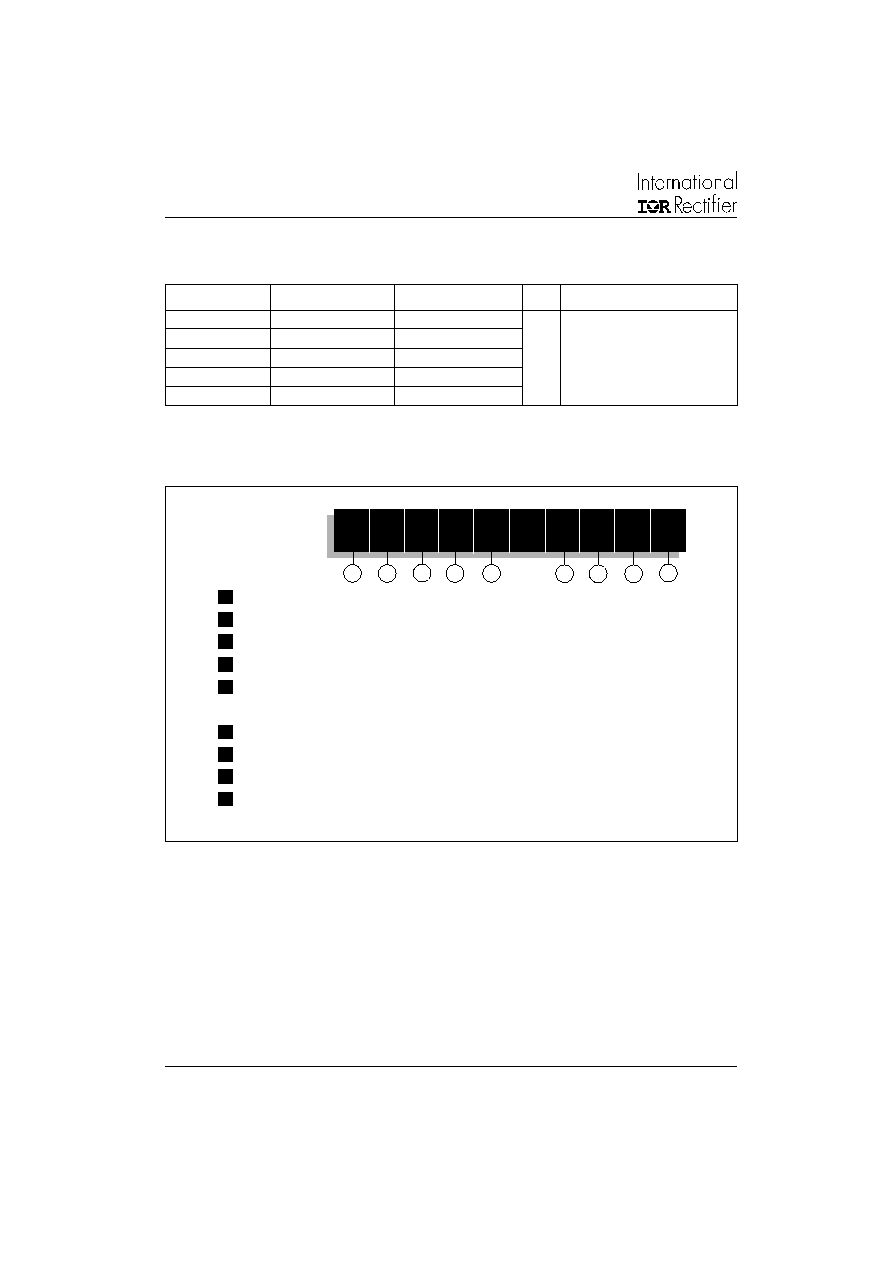
IRK
T
F
13
2
-
08
H
L
N
1
2
3
1
- Module type
2
- Circuit configuration
3
- Fast SCR
4
- Current rating: I
T(AV)
x 10 rounded
5
- 1 =
option with spacers and longer terminal screws
2 =
option with standard terminal screws
6
- Voltage code: Code x 100 = V
RRM
(See Voltage Ratings Table)
7
- dv/dt code: H
400V/µs
8
- t
q
code: L
15µs
9
- None = Standard devices
N
= Aluminum nitrade substrate
4
Device Code
Ordering Information Table
5
6
7
8
8
NOTE: To order the Optional Hardware see Bulletin I27900

IRK.F132.. Series
5
Bulletin I27092 rev. A 09/97
www.irf.com
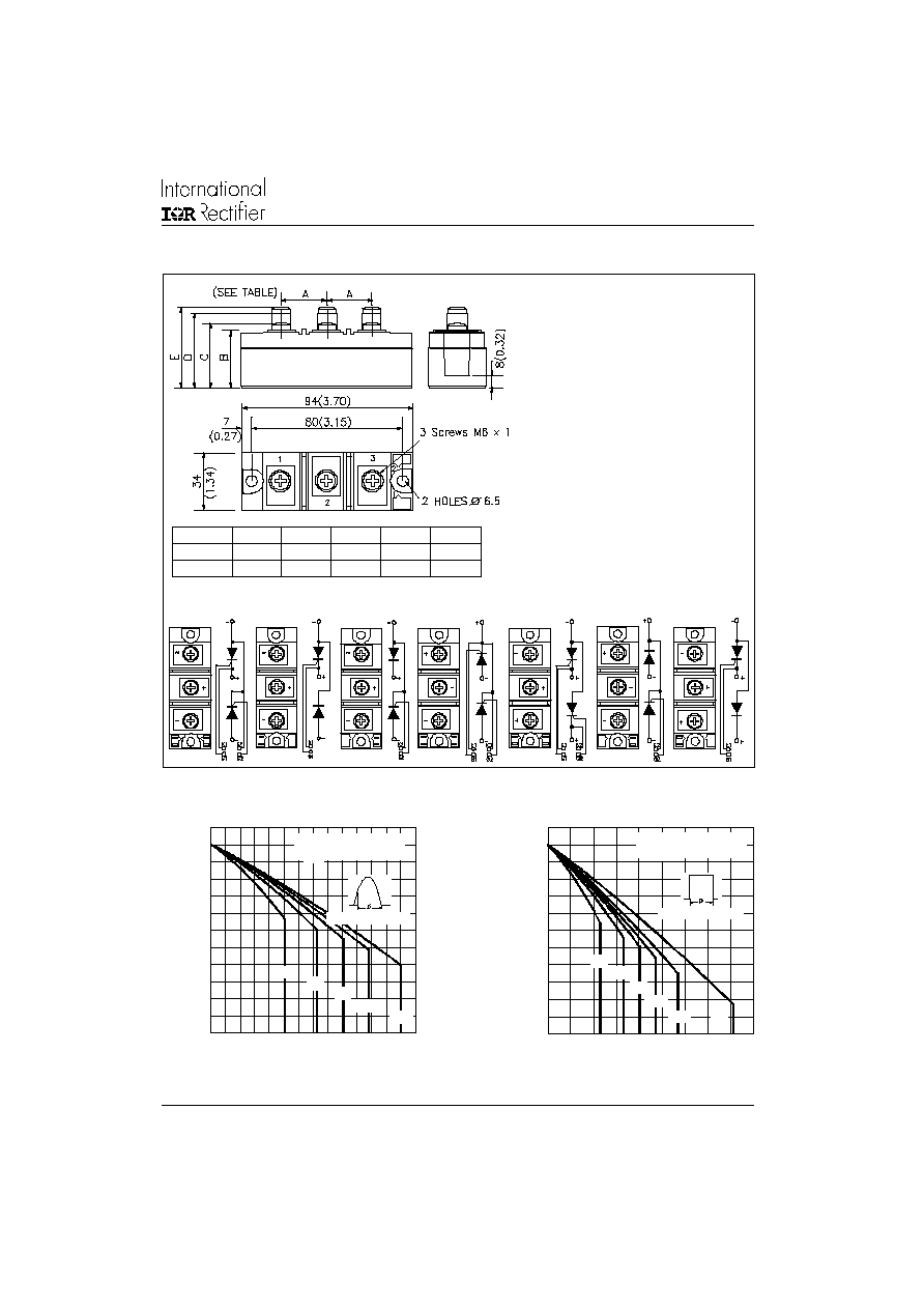
- All dimensions in millimeters (inches)
- Dimensions are nominal
- Full engineering drawings are available
on request
- UL identification number for gate and
cathode wire: UL 1385
- UL identification number for package:
UL 94V0
Outline Table
For all types
A
B
C
D
E
IRK...1
25 (0.98)
----
----
41 (1.61)
47 (1.85)
IRK...2
23 (0.91)
30 (1.18)
36 (1.42)
----
----
IRKTF..
IRKHF..
IRKLF..
IRKUF..
IRKVF..
IRKKF..
IRKNF..
Fig. 1 - Current Ratings Characteristics
Fig. 2 - Current Ratings Characteristics
70
80
90
100
110
120
130
0
20
40
60
80
100
120
140
30∞
60∞
90∞
120∞
180∞
Average On-state Current (A)
M
a
x
i
mu
m
A
l
l
o
w
a
b
l
e
C
a
s
e
T
e
mp
e
r
a
t
u
r
e
(
∞C
)
Conduction Angle
IRK.F132.. Series
R (DC) = 0.17 K/W
thJC
70
80
90
100
110
120
130
0
25
50
75 100 125 150 175 200 225
DC
30∞
60∞
90∞
120∞
180∞
Average On-state Current (A)
M
a
x
i
m
u
m
A
llo
w
a
b
l
e C
a
s
e
T
e
m
p
er
a
t
u
r
e (
∞C
)
Conduction Period
IRK.F132.. Series
R (DC) = 0.17 K/W
thJC
