Features
High voltage
Electrically isolated base plate
3000 V
RMS
isolating voltage
Industrial standard package
Simplified mechanical designs, rapid assembly
High surge capability
Large creepage distances
UL E78996 approved
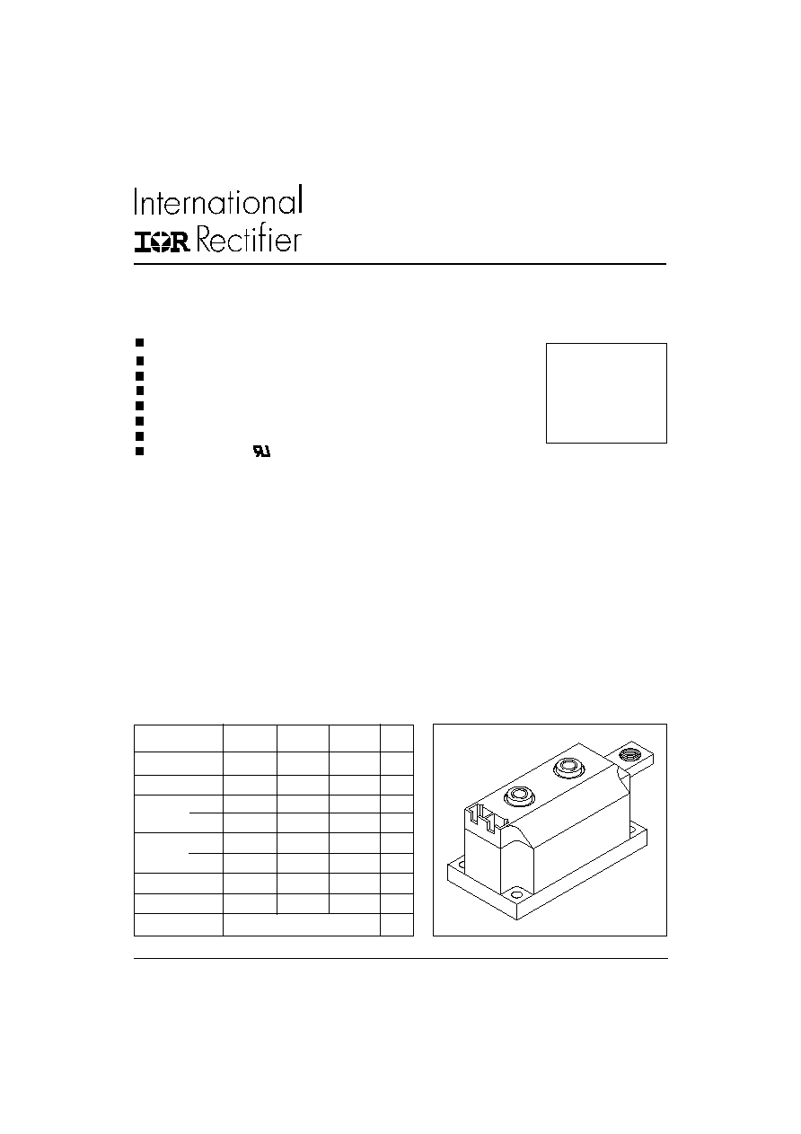
This new IRK serie of MAGN-A-paks modules uses high
voltage power thyristor/thyristor and thyristor/diode in
seven basic configurations. The semiconductors are
electrically isolated from the metal base, allowing com-
mon heatsinks and compact assemblies to be built. They
can be interconnected to form single phase or three
phase bridges or as AC-switches when modules are
connected in anti-parallel mode.
These modules are intended for general purpose appli-
cations such as battery chargers, welders and plating
equipment and where high voltage and high current are
required (motor drives, U.P.S., etc.).
Description
I
T(AV)
@ 85∞C
170
230
250
A
I
T(RMS)
377
510
555
A
I
TSM
@ 50Hz
5100
7500
8500
A
@ 60Hz
5350
7850
8900
A
I
2
t
@ 50Hz
131
280
361
KA
2
s
@ 60Hz
119
256
330
KA
2
s
I
2
t
1310
2800
3610
KA
2
s
V
DRM
/ V
RRM
Up to1600 Up to 2000 Up to1600
V
T
J
range
-40 to 130
o
C
Parameters
IRK.170..
IRK.230.. IRK.250..
Units
Major Ratings and Characteristics
SCR / SCR and SCR / DIODE
170A
230A
250A
MAGN-A-pak
Power Modules
IRK. SERIES
1
Bulletin I27102 rev. C 05/02
www.irf.com

IRK.170, .230, .250 Series
2
Bulletin I27102 rev. C 05/02
www.irf.com
Parameters
IRK.170 IRK.230 IRK.250
Units Conditions
I
T(AV)
Maximum average on-state current
170
230
250
A
180
o
conduction, half sine wave
@ Case temperature
85
85
85
o
C
I
T(RMS)
Maximum RMS on -state current
377
510
555
A
as AC switch
I
TSM
Maximum peak, one-cycle on-state,
5100
7500
8500
A
t = 10ms No voltage
non-repetitive surge current
5350
7850
8900
t = 8.3ms reapplied
4300
6300
7150
t = 10ms 100% V
RRM
4500
6600
7500
t = 8.3ms reapplied
Sinusoidal half wave,
I
2
t
Maximum I
2
t for fusing
131
280
361
KA
2
s t = 10ms No voltage initial T
J
= T
J
max
119
256
330
t = 8.3ms reapplied
92.5
198
255
t = 10ms 100% V
RRM
84.4
181
233
t = 8.3ms reapplied
I
2
t
Maximum I
2
t for fusing
1310
2800
3610
KA
2
s t = 0.1 to 10ms, no voltage reapplied
V
T(TO)1
Low level value of threshold voltage
0.89
1.03
0.97
V
(16.7% x
x I
T(AV)
< I <
x I
T(AV)
), T
J
= T
J
max.
V
T(TO)2
High level value of threshold voltage
1.12
1.07
1.00
(I >
x I
T(AV)
), T
J
= T
J
max.
r
t1
Low level on-state slope resistance
1.34
0.77
0.60
m
(16.7% x
x I
T(AV)
< I <
x I
T(AV)
), T
J
= T
J
max.
r
t2
High level on-state slope resistance
0.96
0.73
0.57
(I >
x I
T(AV)
), T
J
= T
J
max.
I
TM
=
x I
T(AV)
, T
J
= T
J
max., 180
o
conduction
Av. power = V
T(TO)
x I
T(AV)
+ r
f
x (I
T(RMS)
)
2
I
H
Maximum holding current
500
500
500
mA Anode supply=12V, initial I
T
=30A, T
J
=25
o
C
I
L
Maximum latching current
1000
1000
1000
Anode supply=12V, resistive load=1
gate pulse: 10V, 100
µ
s, T
J
= 25∞C
Type number
Voltage
V
RRM
V
DRM
, maximum
V
RSM
, maximum non-repetitive
I
RRM
I
DRM
max
Code
repetitive peak reverse and
peak reverse voltage
@ 130∞C
off-state blocking voltage
V
V
m A
04
400
500
50
IRK.170-
08
800
900
IRK.250-
12
1200
1300
14
1400
1500
16
1600
1700
IRK.230-
08
800
900
50
12
1200
1300
16
1600
1700
18
1800
1900
20
2000
2100
t
d
Typical delay time
1.0
µ
s
T
J
= 25
o
C, Gate Current=1A dI
g/dt
=1A/µs
t
r
Typical rise time
2.0
Vd = 0,67% V
DRM
I
TM
= 300 A ; -dI/dt=15 A/µs; T
J
= T
J
max ;
Vr = 50 V; dV/dt = 20 V/µs ; Gate 0 V, 100 ohm
Voltage Ratings
ELECTRICAL SPECIFICATIONS
On-state Conduction
Switching
t
q
Typical turn-off time
50 - 150
µ
s
V
TM
Maximum on-state voltage drop
1.60
1.59
1.44
V
Parameters
IRK.170 IRK.230 IRK.250
Units Conditions

IRK.170, .230, .250 Series
3
Bulletin I27102 rev. C 05/02
www.irf.com
I
RRM
Max. peak reverse and off-state
50
mA T
J
=T
J
max.
I
DRM
leakage current
V
INS
RMS isolation voltage
3000
V
50Hz, circuit to base, all termin. shorted, 25∞C,1s
dv/
dt
Critical rate of rise of off-state voltage
1000
V/
µ
s T
J
= T
J
max, exponential to 67% rated V
DRM
T
J
Junction operating temperature
-40 to 130
o
C
T
stg
Storage temperature range
-40 to 150
o
C
R
thJC
Maximum thermal resistance
junction to case
Mounting surface flat, smooth and greased
(per module)
T
Mounting tourque ±10%
A mounting compound is recommended and the
MAP to heatsink
4 to 6
Nm tourque should be rechecked after a period of
Busbar to MAP
4 to 6
Nm about 3 hours to allow for the spread of the
compound
wt
Approximate weight
500
g
17.8
oz
Case style
MAGN-A-pak
I
P
GM
Maximum peak gate power
10.0
W
tp
5ms,
T
J
= T
J
max.
P
G(AV)
Maximum average gate power
2.0
W
f = 50Hz,
T
J
= T
J
max.
+I
GM
Maximum peak gate current
3.0
A
tp
5ms,
T
J
= T
J
max.
-V
GT
Max. peak negative gate voltage
5.0
V
tp
5ms,
T
J
= T
J
max.
V
GT
Maximum required DC gate
4.0
V
T
J
= - 40
o
C
Anode supply = 12V, resistive
voltage to trigger
3.0
V
T
J
= 25
o
C
load ; Ra = 1
2.0
V
T
J
= T
J
max.
I
GT
Maximum required DC gate
350
mA
T
J
= - 40
o
C
Anode supply = 12V, resistive
current to trigger
200
mA
T
J
= 25
o
C
load ; Ra = 1
100
mA
T
J
= T
J
max.
V
GD
Maximum gate voltage
that will not trigger
I
GD
Maximum gate current
that will not trigger
di/
dt
Max rate of rise of
turned-on current
Blocking
Triggering
Thermal and Mechanical Specifications
0.25
V
@ T
J
= T
J
max., rated V
DRM
applied
10.0
mA @ T
J
= T
J
max., rated V
DRM
applied
500
A/
µ
s @ T
J
= T
J
max., I
TM
= 400 A rated V
DRM
applied
0.17
0.125
0.125
K/W Per junction, DC operation
R
thC-S
Thermal resistance, case to heatsink
0.02
0.02
0.02
K/W
Parameters
IRK.170 IRK.230 IRK.250
Units Conditions
Parameters
IRK.170 IRK.230 IRK.250
Units Conditions
Parameters
IRK.170 IRK.230 IRK.250
Units Conditions

IRK.170, .230, .250 Series
4
Bulletin I27102 rev. C 05/02
www.irf.com
Thyristor
Diode
I
T(AV)
/ I
F(AV)
@ T
C
V
DRM
V
RSM
V
RRM
170A
230A
250A
V
RRM
V
RSM
@ 85∞C
@ 85∞C
@ 85∞C
1400
1500
2000
IRKH170-14D20
IRKH230-14D20
IRKH250-14D20
1400
1500
2000
IRKL170-14D20
IRKL230-14D20
IRKL250-14D20
1600
1700
2500
IRKH170-16D25
IRKH230-16D25
IRKH250-16D25
1600
1700
2500
IRKL170-16D25
IRKL230-16D25
IRKL250-16D25
1800
1900
2800
Not Available
IRKH230-18D28
Not Available
1800
1900
2800
Not Available
IRKL230-18D28
Not Available
2000
2100
3200
Not Available
IRKH230-20D32
Not Available
2000
2100
3200
Not Available
IRKL230-20D32
Not Available
M
3 x IRKL...
3 x IRKH...
3 x IRKT...
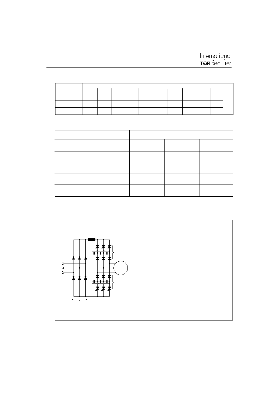
Current-Source Inverters (also known as Sequentially
Commutated Inverters) use Phase Control (as op-
posed to Fast) Thyristors and Diodes.
The advantages of Current Source Inverters lie in their
ease control, absence of large commutation induc-
tances and limited fault currents.
Their simple construction, illustrated by the circuit on
the left, is further enhanced by the use of MAGN-A-
paks which allow the power circuit of an Inverter to be
realised with 6 capacitors and 9 MAGN-A-paks all
mounted on just one heatsink.
The optimal design of Current Source Inverters re-
quires the use of Diodes with blocking voltages greater
than those of the thyristors .
This departure from conventional half-bridge modules
is catered for by MAGN-A-pak range with Thyristors up
to 2000V and Diodes up to 3200V.
Current Source Inverters
Current Source Inverter using 9 MAGN-A-paks
MAGN-A-paks Suitable for Current Source Inverters
Application Notes
For all other parameters and characteristics refer to standard IRKH... and IRKL... modules.
Sinusoidal conduction @ T
J
max.
Rectangular conduction @ T
J
max.
Devices
Units
180
o
120
o
90
o
60
o
30
o
180
o
120
o
90
o
60
o
30
o
IRK.170-
0.009
0.010
0.010
0.020
0.032
0.007
0.011
0.015
0.020
0.033 K/W
IRK.230-
0.009
0.010
0.010
0.020
0.032
0.007
0.011
0.015
0.020
0.033
IRK.250-
0.009
0.010
0.014
0.020
0.032
0.007
0.011
0.015
0.020
0.033
R Conduction (per Junction)
(The following table shows the increment of thermal resistance R
thJC
when devices operate at different conduction angles than DC)

IRK.170, .230, .250 Series
5
Bulletin I27102 rev. C 05/02
www.irf.com
IRK
T
250
-
14 D20
1
-
Module type
2
-
Circuit configuration (See Outline Table)
3
-
Current rating
4
-
Voltage code: Code x 100 = V
RRM
(See Voltage Ratings Table)
5
-
Current Source Inverters Types
Ordering Information Table
Device Code
1
3
4
5
2
IRKL...
IRKU...
IRKV...
IRKK...
IRKN...
IRKH...
IRKT...
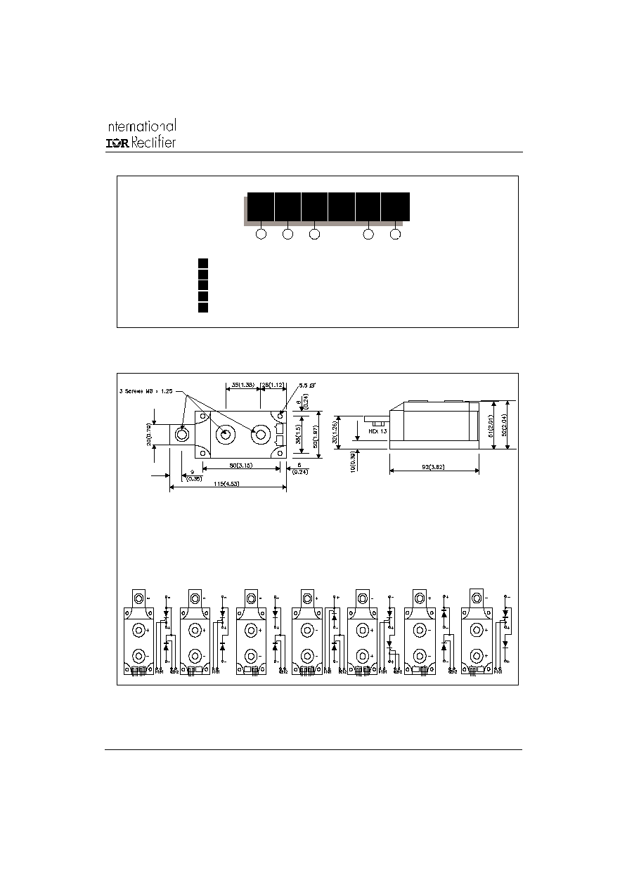
- All dimensions in millimeters (inches)
- Dimensions are nominal
- Full engineering drawings are available
on request
- UL identification number for gate
and cathode wire: UL 1385
- UL identification number for package:
UL 94V0
Outline Table
NOTE: To order the Optional Hardware see Bulletin I27900
