 | –≠–ª–µ–∫—Ç—Ä–æ–Ω–Ω—ã–π –∫–æ–º–ø–æ–Ω–µ–Ω—Ç: IRKU71 | –°–∫–∞—á–∞—Ç—å:  PDF PDF  ZIP ZIP |

Parameters IRKU/V71 IRKU/V91
Units
I
T(AV)
@ 85∞C
75
95
A
I
T(RMS)
115
150
A
I
TSM
@ 50Hz
1665
1785
A
@ 60Hz
1740
1870
A
I
2
t
@ 50Hz
13.86
15.91
KA
2
s
@ 60Hz
12.56
14.52
KA
2
s
I
2
t
138.6
159.1
KA
2
s
V
RRM
range
400 to 1600
V
T
STG
- 40 to 125
o
C
T
J
- 40 to125
o
C
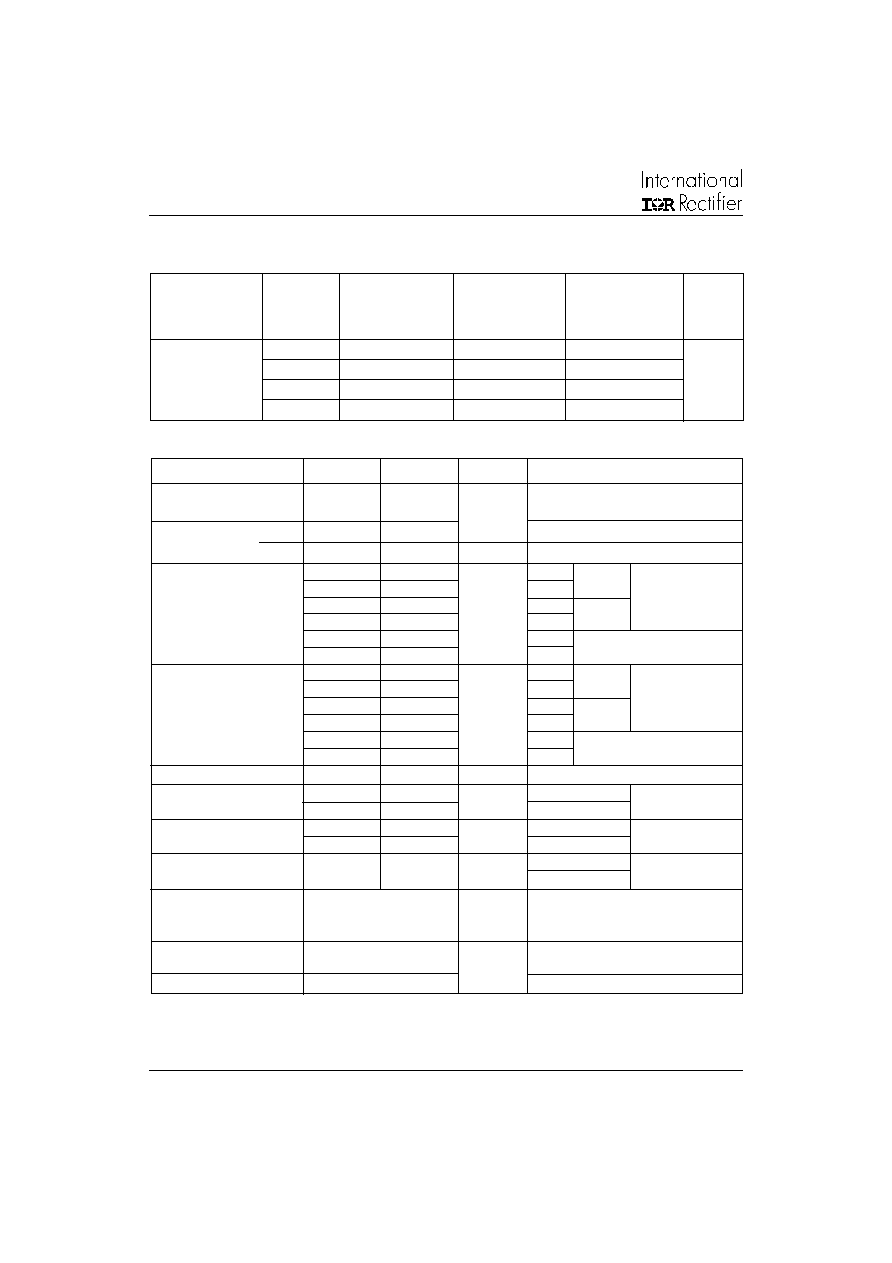
Major Ratings and Characteristics
75 A
95 A
ADD-A-pak
TM
GEN V Power Modules
THYRISTOR/ THYRISTOR
IRKU/V71, 91 SERIES
1
Bulletin I27135 rev. F 10/02
www.irf.com
Features
High Voltage
Industrial Standard Package
Thick Al metal die and double stick bonding
Thick copper baseplate
UL E78996 approved
3500V
RMS
isolating voltage
Benefits
Up to 1600V
Full compatible TO-240AA
High Surge capability
Easy Mounting on heatsink
Al
2
0
3
DBC insulator
Heatsink grounded
Mechanical Description
The Generation V of Add-A-pak module combine the
excellent thermal performance obtained by the usage of
Direct Bonded Copper substrate with superior
mechanical ruggedness, thanks to the insertion of a solid
Copper baseplate at the bottom side of the device.
The Cu baseplate allow an easier mounting on the
majority of heatsink with increased tolerance of surface
roughness and improve thermal spread.
The Generation V of AAP module is manufactured
without hard mold, eliminating in this way any possible
direct stress on the leads.
Electrical Description
These modules are intended for general purpose high
voltage applications such as high voltage regulated power
supplies, lighting circuits, temperature and motor speed
control circuits, UPS and battery charger.
The electrical terminals are secured against axial pull-out:
they are fixed to the module housing via a click-stop
feature already tested and proved as reliable on other IR
modules.
IRKU/V71, 91 Series
2
Bulletin I27135 rev. F 10/02
www.irf.com
V
RRM
, maximum
V
RSM
, maximum
V
DRM
, max. repetitive
I
RRM
Voltage
repetitive
non-repetitive
peak off-state voltage,
I
DRM
Code
peak reverse voltage peak reverse voltage
gate open circuit
125∞C
-
V
V
V
mA
04
400
500
400
IRKU/V71, 91
08
800
900
800
15
12
1200
1300
1200
16
1600
1700
1600
ELECTRICAL SPECIFICATIONS
Voltage Ratings
Type number
I
T(AV)
Max. average on-state
75
95
180
o
conduction, half sine wave,
current
T
C
= 85
o
C
I
T(RMS
)
Max. RMS on-state
115
150
DC
current
@T
C
80
75
∞C
I
TSM
Max. peak, one cycle
1665
1785
t=10ms No voltage
non-repetitive on-state
1740
1870
t=8.3ms reapplied
current
1400
1500
t=10ms 100% V
RRM
1470
1570
t=8.3ms reapplied
1850
2000
t=10ms T
J
= 25
o
C,
1940
2100
t=8.3ms no voltage reapplied
I
2
t
Max. I
2
t for fusing
13.86
15.91
t=10ms No voltage
12.56
14.52
t=8.3ms reapplied
9.80
11.25
t=10ms 100% V
RRM
8.96
10.27
t=8.3ms reapplied
17.11
20.00
t=10ms T
J
= 25
o
C,
15.60
18.30
t=8.3ms no voltage reapplied
I
2
t
Max. I
2
t for fusing (1)
138.6
159.1
KA
2
s
t=0.1 to 10ms, no voltage reapplied
V
T(TO)
Max. value of threshold
0.82
0.80
Low level (3)
voltage (2)
0.85
0.85
High level (4)
r
t
Max. value of on-state
3.00
2.40
Low level (3)
slope resistance (2)
2.90
2.25
High level (4)
V
TM
Max. peak on-state
I
TM
=
x I
T(AV)
voltage
I
FM
=
x I
F(AV)
di/dt
Max. non-repetitive rate
T
J
= 25
o
C, from 0.67 V
DRM
,
of rise of turned on
I
TM
=
x I
T(AV)
,
I
g
= 500mA,
current
t
r
< 0.5 µs, t
p
> 6 µs
T
J
= 25
o
C, anode supply = 6V,
resistive load, gate open circuit
I
L
Max. latching current
400
T
J
= 25
o
C, anode supply = 6V,resistive load
T
J
= T
J
max
T
J
= T
J
max
(1) I
2
t for time t
x
= I
2
t
x
t
x
.
(2) Average power =
V
T(TO)
x
I
T(AV)
+
r
t
x
(
I
T(RMS)
)
2
(3) 16.7%
x
x I
AV
< I <
x I
AV
(4)
I >
x I
AV
I
H
Max. holding current
200
Initial T
J
= T
J
max.
150
A/µs
KA
2
s
V
m
mA
Sinusoidal
half wave,
Initial T
J
= T
J
max.
Parameters
IRKU/V71
IRKU/V91
Units
Conditions
On-state Conduction
A
A
1.59
1.58
V
T
J
= 25∞C
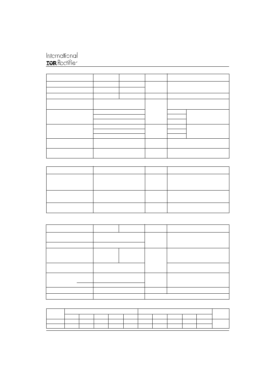
IRKU/V71, 91 Series
3
Bulletin I27135 rev. F 10/02
www.irf.com
I
RRM
Max. peak reverse and
I
DRM
off-state leakage current
at V
RRM
, V
DRM
2500 (1 min)
50 Hz, circuit to base, all terminals
3500 (1 sec)
shorted
dv/dt Max. critical rate of rise
T
J
= 125
o
C, linear to 0.67 V
DRM
,
of off-state voltage (5)
gate open circuit
T
J
Junction operating
temperature range
T
stg
Storage temper. range
- 40 to 125
R
thJC
Max. internal thermal
resistance, junction
0.165
0.135
Per module, DC operation
to case
R
thCS
Typical thermal resistance
case to heatsink
T
Mounting torque ± 10%
to heatsink
busbar
3
wt Approximate weight
110 (4)
gr (oz)
Case style
TO-240AA
JEDEC
15
mA
T
J
= 125
o
C, gate open circuit
Thermal and Mechanical Specifications
Parameters
IRK.71
IRK.91
Units
Conditions
- 40 to 125
0.1
5
Triggering
(5) Available with dv/dt = 1000V/
µ
s, to complete code add S90 i.e. IRKU91/16AS90.
A mounting compound is recommended
and the torque should be rechecked after
a period of 3 hours to allow for the spread
of the compound
∞C
K/W
Nm
Mounting surface flat, smooth and greased
V
INS
RMS isolation voltage
V
P
GM
Max. peak gate power
12
12
P
G(AV)
Max. average gate power
3.0
3.0
I
GM
Max. peak gate current
3.0
3.0
A
-V
GM
Max. peak negative
gate voltage
4.0
T
J
= - 40∞C
2.5
T
J
= 25∞C
1.7
T
J
= 125∞C
270
T
J
= - 40∞C
150
mA
T
J
= 25∞C
80
T
J
= 125∞C
V
GD
Max. gate voltage
that will not trigger
I
GD
Max. gate current
that will not trigger
Parameters
IRKU/V71
IRKU/V91
Units
Conditions
0.25
V
6
mA
Anode supply = 6V
resistive load
V
GT
Max. gate voltage
required to trigger
Anode supply = 6V
resistive load
I
GT
Max. gate current
required to trigger
W
V
10
T
J
= 125
o
C,
rated V
DRM
applied
T
J
= 125
o
C,
rated V
DRM
applied
500
V/
µ
s
Parameters
IRKU/V71, 91
Units
Conditions
Blocking
Sine half wave conduction
Rect. wave conduction
Devices
Units
180
o
120
o
90
o
60
o
30
o
180
o
120
o
90
o
60
o
30
o
IRKU/V71
0.06
0.07
0.09
0.12
0.18
0.04
0.08
0.10
0.13
0.18
IRKU/V91
0.04
0.05
0.06
0.08
0.12
0.03
0.05
0.06
0.08
0.12
∞C/W
R Conduction (per Junction)
(The following table shows the increment of thermal resistance R
thJC
when devices operate at different conduction angles than DC)

IRKU/V71, 91 Series
4
Bulletin I27135 rev. F 10/02
www.irf.com
K1
G1
(4) (5)
+
K2
G2
-
-
(1)
(2)
(3)
(7) (6)
+
K2 G2
-
K1
G1
+
(1)
(2)
(4) (5)
(7) (6)
(3)
Outline Table
Dimensions are in millimeters and [inches]
IRKU
IRKV
NOTE: To order the Optional Hardware see Bulletin I27900
IRK
U
91
/
16
A S90
Device Code
1
2
3
4
5
1
-
Module type
2
-
Circuit configuration (See Circuit Configuration table)
3
-
Current code * *
4
-
Voltage code (See Voltage Ratings table)
5
-
A : Gen V
6
-
dv/dt code:
S90 = dv/dt 1000 V/µs
No letter = dv/dt 500 Vµs
Ordering Information Table
6
* * Available with no auxiliary cathode.
To specify change:
91 to 92
71 to 72
e.g. : IRKU92/16A etc.
IRK.92 types
With no auxiliary cathode

IRKU/V71, 91 Series
5
Bulletin I27135 rev. F 10/02
www.irf.com
Fig. 1 - Current Ratings Characteristics
Fig. 2 - Current Ratings Characteristics
Fig. 3 - On-state Power Loss Characteristics
Fig. 4 - On-state Power Loss Characteristics
70
80
90
100
110
120
130
0
10
20
30
40
50
60
70
80
M
a
x
i
m
u
m
A
llo
w
a
b
l
e C
a
s
e
T
e
m
p
e
r
at
u
r
e (
∞
C
)
30∞
60∞ 90∞
120∞
180∞
Average On-state Current (A)
Conduction Angle
IRK.71.. Series
R (DC) = 0.33 K/W
thJC
70
80
90
100
110
120
130
0
20
40
60
80
100
120
DC
30∞
60∞
90∞
120∞
180∞
Average On-state Current (A)
Ma
x
i
m
u
m
Al
l
o
wab
l
e
Ca
s
e
T
e
m
p
er
a
t
u
r
e (
∞
C
)
Conduction Period
IRK.71.. Series
R (DC) = 0.33 K/W
thJC
0
20
40
60
80
100
120
0
10
20
30
40
50
60
70
80
180∞
120∞
90∞
60∞
30∞
RMS Limit
Conduction Angle
M
a
x
i
m
u
m
A
v
er
a
g
e On-s
t
a
t
e
Po
w
e
r
L
o
s
s
(
W
)
Average On-state Current (A)
IRK.71.. Series
Per Junction
T = 125∞C
J
0
20
40
60
80
100
120
140
0
20
40
60
80
100
120
DC
180∞
120∞
90∞
60∞
30∞
RMS Limit
Conduction Period
Max
i
m
u
m
A
v
er
ag
e On
-s
t
a
t
e
P
o
w
e
r
L
o
s
s
(
W
)
Average On-state Current (A)
IRK.71.. Series
Per Junction
T = 125∞C
J
Fig. 5 - Maximum Non-Repetitive Surge Current
Fig. 6 - Maximum Non-Repetitive Surge Current
700
800
900
1000
1100
1200
1300
1400
1500
1600
1
10
100
Number Of Equal Amplitude Half Cycle Current Pulses (N)
P
e
ak
Hal
f
S
i
n
e
W
a
v
e
O
n
-
s
t
a
t
e
C
u
r
r
e
n
t
(
A
)
Initial T = 125∞C
@ 60 Hz 0.0083 s
@ 50 Hz 0.0100 s
J
At Any Rated Load Condition And With
Rated V Applied Following Surge.
RRM
IRK.71.. Series
Per Junction
600
800
1000
1200
1400
1600
1800
0.01
0.1
1
P
e
a
k
H
a
l
f
S
i
n
e
W
a
v
e
O
n
-
s
t
a
t
e
Cu
r
r
en
t
(
A
)
Pulse Train Duration (s)
Initial T = 125∞C
No Voltage Reapplied
Rated V Reapplied
Of Conduction May Not Be Maintained.
RRM
J
Maximum Non Repetitive Surge Current
Versus Pulse Train Duration. Control
IRK.71.. Series
Per Junction