Data Sheet No.PD60267
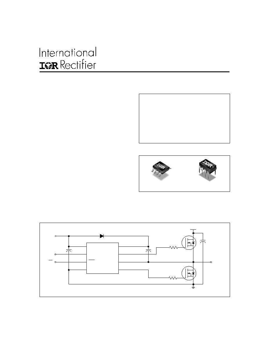
Typical Connection
Product Summary
V
OFFSET
600 V max.
I
O
+/-
130 mA/270 mA
V
OUT
10 V - 20 V
t
on/off
(typ.)
680 ns/150 ns
Deadtime (typ.)
520 ns
HALF-BRIDGE DRIVER
Features
∑
Floating channel designed for bootstrap operation
∑
Fully operational to +600 V
∑
Tolerant to negative transient voltage, dV/dt
immune
∑
Gate drive supply range from 10 V to 20 V
∑
Undervoltage lockout
∑
3.3 V, 5 V, and 15 V input logic compatible
∑
Cross-conduction prevention logic
∑
Internally set deadtime
∑
High side output in phase with input
∑
Shutdown input turns off both channels
∑
Matched propagation delay for both channels
Description
The IRS2104 is a high voltage, high speed power
MOSFET and IGBT driver with dependent high and low
side referenced output channels. Proprietary HVIC and
latch immune CMOS technologies enable ruggedized
monolithic construction. The logic input is compatible
with standard CMOS or LSTTL output, down to 3.3 V
logic. The output drivers feature a high pulse current buffer stage designed for minimum driver cross-
conduction. The floating channel can be used to drive an N-channel power MOSFET or IGBT in the high side
configuration which operates from 10 V to 600 V.
www.irf.com
1
IRS2104(S)PbF
V
CC
V
B
V
S
HO
LO
COM
IN
SD
SD
IN
up to 600 V
TO
LOAD
V
CC
(Refer to Lead Assignment for correct pin configuration). This diagram shows electrical
connections only. Please refer to our Application Notes and DesignTips for proper circuit board layout.
Packages
8 Lead PDIP
IRS2104
8 Lead SOIC
IRS2104S
IRS2104(S) PbF
www.irf.com
2
Symbol
Definition
Min.
Max.
Units
V
B
High side floating absolute voltage
-0.3
625
V
S
High side floating supply offset voltage
V
B
- 25
V
B
+ 0.3
V
HO
High side floating output voltage
V
S
- 0.3
V
B
+ 0.3
V
CC
Low side and logic fixed supply voltage
-0.3
25
V
LO
Low side output voltage
-0.3
V
CC
+ 0.3
V
IN
Logic input voltage (IN &
SD
)
-0.3
V
CC
+ 0.3
dV
s
/dt
Allowable offset supply voltage transient
--
50
V/ns
P
D
Package power dissipation @ T
A
+25
∞C
(8 lead PDIP)
--
1.0
(8 lead SOIC)
--
0.625
Rth
JA
Thermal resistance, junction to ambient
(8 lead PDIP)
--
125
(8 lead SOIC)
--
200
T
J
Junction temperature
--
150
T
S
Storage temperature
-55
150
T
L
Lead temperature (soldering, 10 seconds)
--
300
Absolute Maximum Ratings
Absolute maximum ratings indicate sustained limits beyond which damage to the device may occur. All voltage
parameters are absolute voltages referenced to COM. The thermal resistance and power dissipation ratings are
measured under board mounted and still air conditions.
Symbol
Definition
Min.
Max.
Units
V
B
High side floating supply absolute voltage
V
S
+ 10
V
S
+ 20
V
S
High side floating supply offset voltage
Note 1
600
V
HO
High side floating output voltage
V
S
V
B
V
CC
Low side and logic fixed supply voltage
10
20
V
LO
Low side output voltage
0
V
CC
V
IN
Logic input voltage (IN &
SD
)
0
V
CC
T
A
Ambient temperature
-40
125
Note 1: Logic operational for V
S
of -5 V to +600 V. Logic state held for V
S
of -5 V to -V
BS
. (Please refer to the Design Tip
DT97-3 for more details).
Recommended Operating Conditions
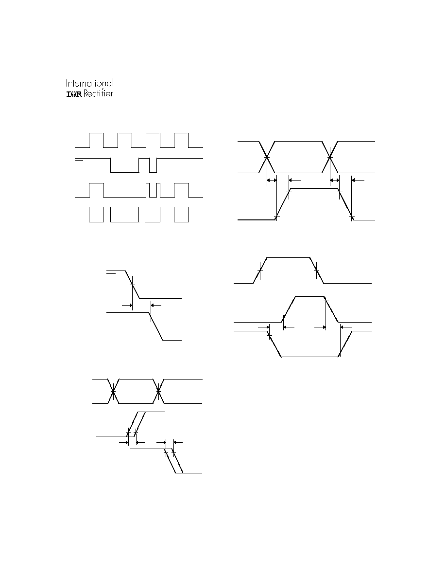
The Input/Output logic timing diagram is shown in Fig.
1. For proper operation the device should be used within the
recommended conditions. The V
S
offset rating is tested with all supplies biased at a 15 V differential.
∞C
V
V
W
∞C/W
∞C
IRS2104(S) PbF
www.irf.com
3
Symbol
Definition
Min. Typ. Max. Units Test Conditions
V
IH
Logic "1" (HO) & Logic "0" (LO) input voltage
2.5
--
--
V
IL
Logic "0" (HO) & Logic "1" (LO) input voltage
--
--
0.8
V
SD,TH+
SD input positive going threshold
2.5
--
--
V
SD,TH-
SD input negative going threshold
--
--
0.8
V
OH
High level output voltage, V
BIAS
- V
O
--
0.05
0.2
V
OL
Low level output voltage, V
O
--
0.02
0.1
I
LK
Offset supply leakage current
--
--
50
V
B
= V
S
= 600 V
I
QBS
Quiescent V
BS
supply current
--
30
55
I
QCC
Quiescent V
CC
supply current
--
150
270
I
IN+
Logic "1" input bias current
--
3
10
V
IN
= 5 V
I
IN-
Logic "0" input bias current
--
--
1
V
IN
= 0 V
V
CCUV+
V
CC
supply undervoltage positive going
8
8.9
9.8
threshold
V
CCUV-
V
CC
supply undervoltage negative going
7.4
8.2
9
threshold
I
O+
Output high short circuit pulsed current
130
290
--
V
O
= 0 V
PW
10
µs
I
O-
Output low short circuit pulsed current
270
600
--
V
O
= 15 V
PW
10
µs
Symbol
Definition
Min. Typ. Max. Units Test Conditions
ton
Turn-on propagation delay
--
680
820
V
S
= 0 V
toff
Turn-off propagation delay
--
150
220
V
S
= 600 V
tsd
Shutdown propagation delay
--
160
220
tr Turn-on rise time -- 70 170
tf Turn-off fall time -- 35 90
DT
Deadtime, LS turn-off to HS turn-on &
400
520
650
HS turn-on to LS turn-off
Static Electrical Characteristics
V
BIAS
(V
CC
, V
BS
) = 15 V and T
A
= 25
∞C unless otherwise specified. The V
IN
, V
TH,
and I
IN
parameters are referenced to
COM. The V
O
and I
O
parameters are referenced to COM and are applicable to the respective output leads: HO or LO.
Dynamic Electrical Characteristics
V
BIAS
(V
CC
, V
BS
) = 15 V, C
L
= 1000 pF and T
A
= 25
∞C unless otherwise specified.
V
V
mA
MT
Delay matching, HS & LS turn-on/off
--
--
60
ns
µA
V
CC
= 10 V to 20 V
I
O
= 2 mA
V
IN
= 0 V or 5 V
IRS2104(S) PbF
www.irf.com
4
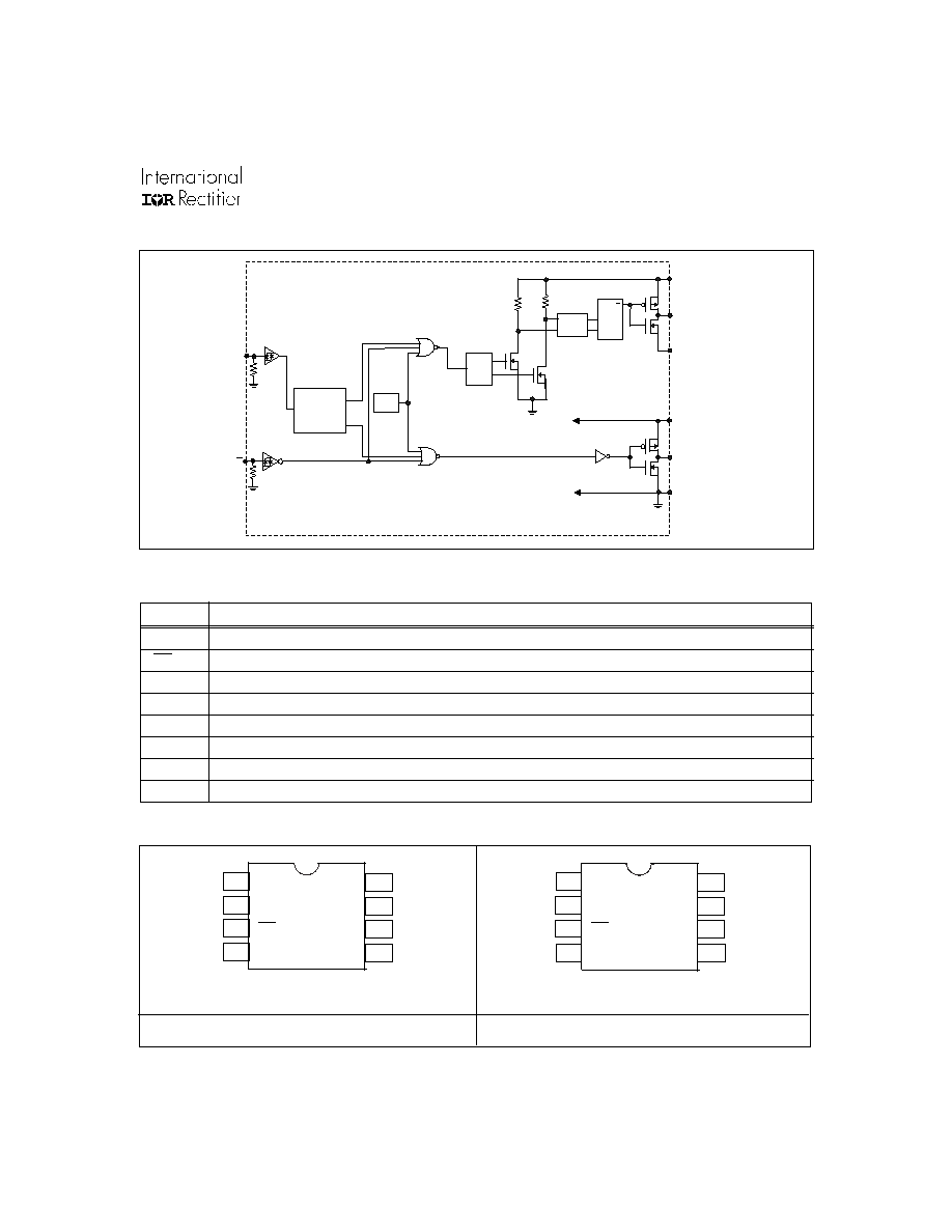
Functional Block Diagram
Lead Definitions
Symbol Description
IN
Logic input for high and low side gate driver outputs (HO and LO), in phase with HO
Logic input for shutdown
V
B
High side floating supply
HO
High side gate drive output
V
S
High side floating supply return
V
CC
Low side and logic fixed supply
LO
Low side gate drive output
COM
Low side return
SD
Lead Assignments
8 Lead PDIP
8 Lead SOIC
IRS2104PbF
IRS2104SPbF
1
2
3
4
8
7
6
5
VCC
IN
SD
COM
VB
HO
VS
LO
1
2
3
4
8
7
6
5
VCC
IN
SD
COM
VB
HO
VS
LO
VB
HO
VS
IN
SD
DEAD TIME &
SHOOT-THROUGH
PREVENTION
PULSE
GEN
PULSE
FILTER
HV
LEVEL
SHIFT
R
S
Q
VCC
LO
COM
UV
DETECT
IRS2104(S) PbF
www.irf.com
5
Figure 5. Delay Matching Waveform Definitions
HO
50%
50%
10%
LO
90%
MT
HO
LO
MT
IN
(LO)
IN
(HO)
Figure 4. Deadtime Waveform Definitions
IN
HO
50%
50%
90%
10%
LO
90%
10%
DT
DT
Figure 3. Shutdown Waveform Definitions
SD
tsd
HO
LO
50%
90%
Figure 1. Input/Output Timing Diagram
SD
IN
HO
LO
Figure 2. Switching Time Waveform Definitions
IN
(HO)
tr
ton
tf
toff
LO
HO
50%
50%
90%
90%
10%
10%
IN
(LO)